UNIT IV MOSFET Circuits Contents MOSFET as diodeactive


 NMOS Amplifier with Enhancement Load • Fig. shows an n-channel enhancement mode MOSFET")
")


 NMOS Amplifier with Depletion Load NMOS amplifier with depletion load device Driver transistor")
 shows an NMOS depletion load amplifier. • Here, T 1")

 is")
 class A amplifier : if the Q point and the input signal are")


 m. V / 0 C")


- Slides: 40
UNIT IV MOSFET Circuits
Contents MOSFET as diode/active resistor, Current Sink and source, Current mirror, Voltage references, Bandgap reference. CMOS Inverter as amplifier: Active load, Current source and Push pull configurations. • Cascode amplifier. • • •
MOSFET as diode/active resistor • When the MOSFET has the gate connected to the drain, it acts like a diode with characteristics similar to a pn-junction diode. MOSFET as diode / active resistor
• Connecting the gate to the drain means that the VDS controls i. D and therefore the channel transconductance becomes a channel conductance. • The small signal conductance can be found by differentiating equation With respect to VGS,
Application of the MOS Diode • Here bias voltage is generated with respect to ground. • VDS=VGS for both the devices. Voltage Division using Active Resistor
Current Sinks or Sources • A current sink and current source are two terminal components whose current at any instant of time is independent of the voltage across their terminals. • The current of a current sink or source flows from the positive node though the sink or source , to the negative node. • A current sink has the negative node at VSS and current source has the positive node at VDD.
Current Sink • The gate is taken to whatever voltage is necessary to create the desired value of current. • The voltage divider can be used to provide this voltage. a) Current Sink
• In the nonsaturation region the MOS device is not a good current source. • The voltage across the current sink must be larger than VMIN, for the current sink to perform properly. b) Current – Voltage Characteristics of Fig. a
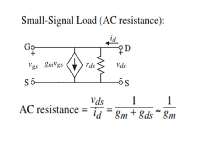
• If the source and bulk both are connected to ground, then small signal output resistance is,
Current Source • Fig. Shows a current source using a p-channel transistor. • Gate is taken to the constant potential as is the source.
• The Source-Drain voltage must be larger than VMIN for the current source to work properly. • This current source only works for values of VOUT given by,
Current Mirror
Simple MOSFET Current Mirror • MOSFET constant-current source uses two MOSFETs T 1 and T 2. • Since the drain and gate of MOSFET T 1 is shorted, it is operated in saturation region. Neglecting channel length modulation (λ=0) the drain current of T 1 is given by
CMOS Inverter • When input is high, transistor Q 1 is OFF ( As source of Q 1 is having more potential than gate) and transistor Q 2 is ON. • As Q 1 is OFF, VOUT = 0.
• When input is low, transistor Q 1 is ON (As gate of p-channel transistor is negative with respect to source) and transistor Q 2 is OFF. • VOUT = VDD • Operation of CMOS Inverter Input Q 1 Q 2 Output 0 (LOW) ON OFF 1 1 (HIGH) OFF ON 0
Amplifiers with Active Load • When MOSFET itself is used as a load device, it is referred to as active load. • There are three types of load devices : 1) n-channel enhancement mode device 2) n-channel depletion-mode device 3) p-channel enhancement mode device
1) NMOS Amplifier with Enhancement Load • Fig. shows an n-channel enhancement mode MOSFET with gate and drain shorted. • In this connection, MOSFET acts as a nonlinear resistor and is called enhancement load device. N-channel enhancement mode MOSFET with gate and drain shorted
• Since MOSFET enhancement VT>0. is in mode, • For this circuit, VDS(Sat) =VGS-VT, which means that MOSFET is biased in saturation region. • The enhancement load circuit alone cannot be used as an amplifier, however, if it is connected in a circuit with another MOSFET, the circuit can be used as an amplifier or as an inverter in a digital circuit. Current-Voltage characteristics for n-channel enhancement load device
• Here, MOSFET T 2 is used as a load and MOSFET T 1 is used as a driver transistor. • The load device T 2 is always biased in the saturation region. NMOS amplifier with enhancement load device Current-Voltage characteristics for n-channel enhancement load device
Small signal equivalent circuit
2) NMOS Amplifier with Depletion Load NMOS amplifier with depletion load device Driver transistor characteristics
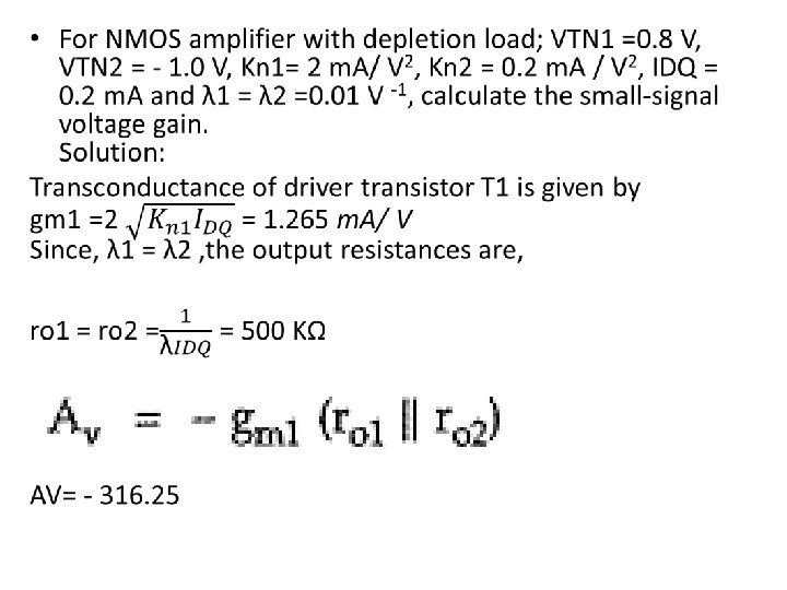
• Fig. (a) shows an NMOS depletion load amplifier. • Here, T 1 is used as a driver and T 2 is used as a load. • Fig. (b) shows the characteristics of T 1 and load curve. • Since the i-v characteristics of the load device is non-linear, the load curve is also non-linear. • Points A and B are transition points for T 1 and T 2, respectively. The Q-point is approximately midway between the two transition points. • For amplifier operation, both MOSFET should be biased in saturation region.
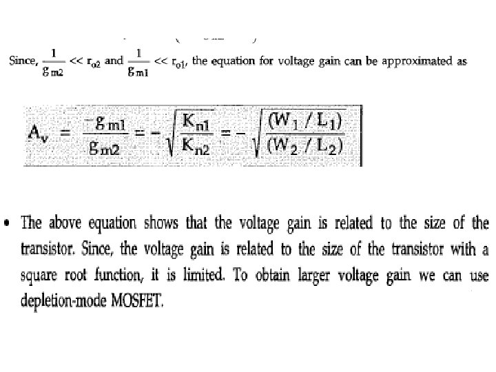
• In the small-signal equivalent circuit of NMOS inverter with depletion load device, • Since the gate to source voltage for depletion load (T 2) is zero, gm. Vgs 2 = 0 Thus, for this circuit, the voltage gain is directly proportional to the output resistances of two transistors.
MOSFET PUSH-PULL Configurations • For an amplifier, a quiescent operating point (Q point) is fixed by selecting the proper d. c. biasing to the transistors used. • The quiescent operating point is shown on the load line, which is plotted on the output characteristics of the transistor. • The position of the quiescent point on the load line decides the class of operation of the power amplifier. • The various classes of the power amplifiers are : i) Class A ii) Class B iii) Class C and iv) Class AB
1) class A amplifier : if the Q point and the input signal are selected such that the output signal is obtained for a full input cycle. 2) class B amplifier : output signal is obtained only for one half cycle for a full input cycle. 3) class C amplifier : the output signal is obtained for less than a half cycle, for a full input cycle. 4) class AB amplifier : the output signal is obtained for more than 180° but less than 360°, for a full input cycle
• The primary advantage of a class B or class AB amplifier over a class A amplifier is that either one is more efficient than a class A amplifier. • A disadvantage of class B or class AB is that it is more difficult to implement the circuit in order to get a linear reproduction of the input waveform. • The term push-pull refers to a common type of class B or class AB amplifier circuit in which the input wave shape is reproduced at the output.
Class B Push-Pull Amplifier • The class B push-pull circuit uses two class B amplifiers, one conducts for the positive half of the cycle and other conducts for the negative half of the cycle to reproduced the entire waveform.
• when the signal exceeds the positive threshold voltage of Q 1, it conducts; • when the signal is below the negative threshold voltage of Q 2 , it conducts. • Thus, the n-channel device conducts on the positive cycle and the p-channel device conducts on the negative cycle.
Voltage References • A voltage reference circuit is basically used to provide a constant d. c. voltage which acts as a reference or standard for other circuits and is independent of changes in the parameters like temperature, input line voltage, load current etc. • The basic requirements of any voltage reference circuit are accuracy and stability with temperature and time.
• The temperature coefficient of the output voltage of a voltage reference circuit is the measure of the ability of the circuit to maintain the standard output voltage under varying temperature conditions. • If V 0 is the output voltage of a voltage reference then mathematically its temperature coefficient is defined as,
• Temperature Coefficient is expressed in – 1) m. V / 0 C or µV / 0 C 2) In % form, % / 0 C 3) In parts per million / 0 C i. e. ppm i. e. by replacing 100 by 106 in the above equation. NOTE: For a good voltage reference circuit, TC must be as low as possible i. e. of the order of few ppm /0 C or less.
Voltage Reference using voltage division • The value of VREF is directly proportional to power supply.
• This relationship can be studied by the concept of Sensitivity, S. • The sensitivity of VREF to VDD can be expressed as • This can be interpreted as: if the sensitivity is 1, then a 10% change in VDD will result in a 10% change in VREF, which is undesirable for a voltage reference.
• A simple way of obtaining a voltage reference is to use an active device =
Bandgap Reference • Bandgap reference has very little dependence on temperature and power supply. • The bandgap reference can generate references having a temperature coefficient on the order of 10 ppm/ 0 C over the temperature range of 0 -70 0 C.
• Voltage VBE is generated from a pn junction diode. • Also generated is a thermal voltage Vt (Vt= k. T/ q), which is proportional to the absolute temperature.
• If the Vt voltage is multiplied by a constant K and summed with the VBE voltage, then the output voltage is given as VREF = VBE + K Vt • Differentiating above equation with respect to temperature and using the temperature coefficients for VBE and Vt leads to a value of K that should theoretically give zero temperature dependence.