UNIT IV Interrupts V SUPRAJA 1 Interrupts are
- Slides: 113

UNIT – IV Interrupts V SUPRAJA 1

Interrupts are commonly used for a range of applications: • Urgent tasks that must be executed promptly at higher priority than the main code. However, it is even faster to execute a task directly by hardware if this is possible. • Infrequent tasks, such as handling slow input from humans. This saves the overhead of regular polling. • Waking the CPU from sleep. This is particularly important in the MSP 430, which typically spends much of its time in a low-power mode and can be awakened only by an interrupt. • Calls to an operating system. These are often processed through a trap or software interrupt instruction but the MSP 430 does not have one. A substitute is for software to set an unused interrupt flag for one of the peripherals, such as port P 1 or P 2. V SUPRAJA 2

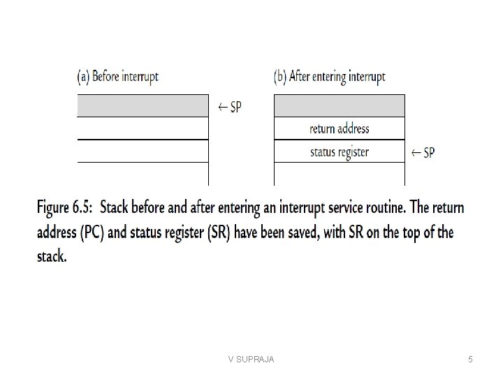
What Happens when an Interrupt Is Requested? • A lengthy chain of operations lies between the cause of a maskable interrupt and the start of its ISR Hardware then performs the following steps to launch the ISR: 1. Any currently executing instruction is completed if the CPU was active when the interrupt was requested. MCLK is started if the CPU was off. 2. The PC, which points to the next instruction, is pushed onto the stack. 3. The SR is pushed onto the stack. 4. The interrupt with the highest priority is selected if multiple interrupts are waiting for service. V SUPRAJA 3

5. The interrupt request flag is cleared automatically for vectors that have a single source. Flags remain set for servicing by software if the vector has multiple sources, which applies to the example of TAIFG. 6. The SR is cleared, which has two effects. First, further maskable interrupts are disabled because the GIE bit is cleared; nonmaskable interrupts remain active. 7. The interrupt vector is loaded into the PC and the CPU starts to execute the interrupt service routine at that address. V SUPRAJA 4

V SUPRAJA 5

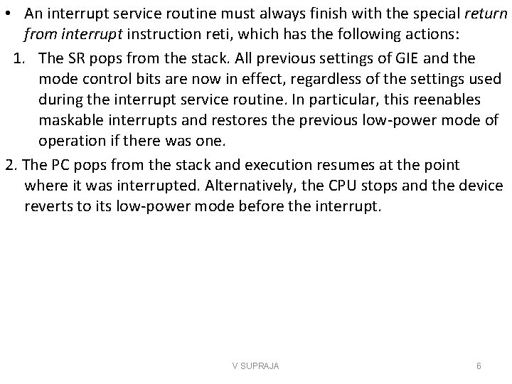
• An interrupt service routine must always finish with the special return from interrupt instruction reti, which has the following actions: 1. The SR pops from the stack. All previous settings of GIE and the mode control bits are now in effect, regardless of the settings used during the interrupt service routine. In particular, this reenables maskable interrupts and restores the previous low-power mode of operation if there was one. 2. The PC pops from the stack and execution resumes at the point where it was interrupted. Alternatively, the CPU stops and the device reverts to its low-power mode before the interrupt. V SUPRAJA 6

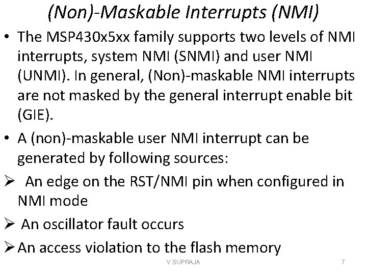
(Non)-Maskable Interrupts (NMI) • The MSP 430 x 5 xx family supports two levels of NMI interrupts, system NMI (SNMI) and user NMI (UNMI). In general, (Non)-maskable NMI interrupts are not masked by the general interrupt enable bit (GIE). • A (non)-maskable user NMI interrupt can be generated by following sources: Ø An edge on the RST/NMI pin when configured in NMI mode Ø An oscillator fault occurs Ø An access violation to the flash memory V SUPRAJA 7

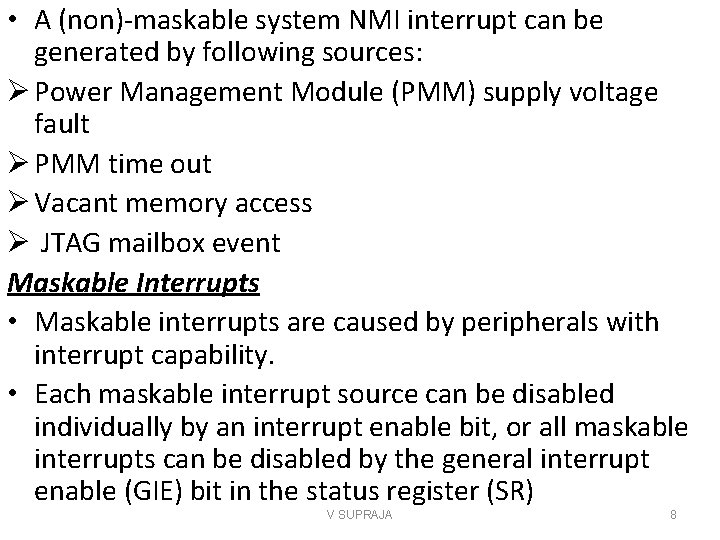
• A (non)-maskable system NMI interrupt can be generated by following sources: Ø Power Management Module (PMM) supply voltage fault Ø PMM time out Ø Vacant memory access Ø JTAG mailbox event Maskable Interrupts • Maskable interrupts are caused by peripherals with interrupt capability. • Each maskable interrupt source can be disabled individually by an interrupt enable bit, or all maskable interrupts can be disabled by the general interrupt enable (GIE) bit in the status register (SR) V SUPRAJA 8

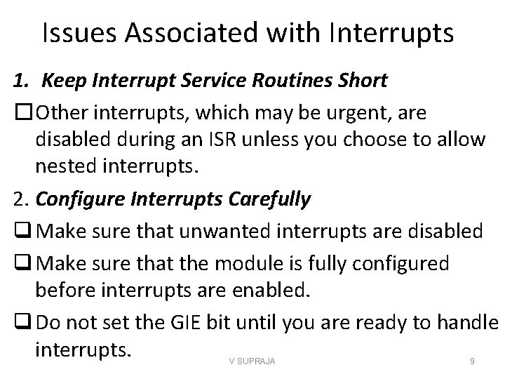
Issues Associated with Interrupts 1. Keep Interrupt Service Routines Short �Other interrupts, which may be urgent, are disabled during an ISR unless you choose to allow nested interrupts. 2. Configure Interrupts Carefully q Make sure that unwanted interrupts are disabled q Make sure that the module is fully configured before interrupts are enabled. q Do not set the GIE bit until you are ready to handle interrupts. V SUPRAJA 9

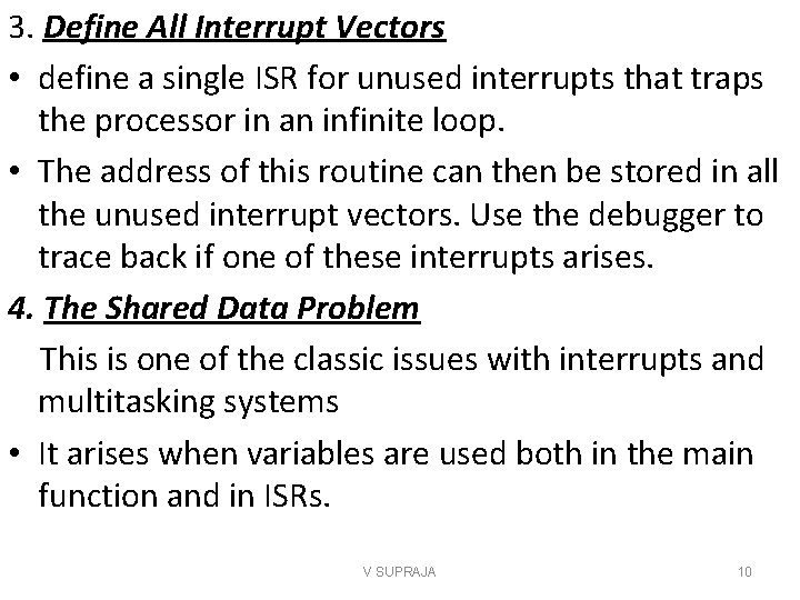
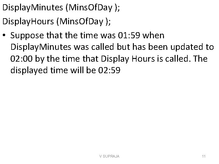
3. Define All Interrupt Vectors • define a single ISR for unused interrupts that traps the processor in an infinite loop. • The address of this routine can then be stored in all the unused interrupt vectors. Use the debugger to trace back if one of these interrupts arises. 4. The Shared Data Problem This is one of the classic issues with interrupts and multitasking systems • It arises when variables are used both in the main function and in ISRs. V SUPRAJA 10

Display. Minutes (Mins. Of. Day ); Display. Hours (Mins. Of. Day ); • Suppose that the time was 01: 59 when Display. Minutes was called but has been updated to 02: 00 by the time that Display Hours is called. The displayed time will be 02: 59 V SUPRAJA 11

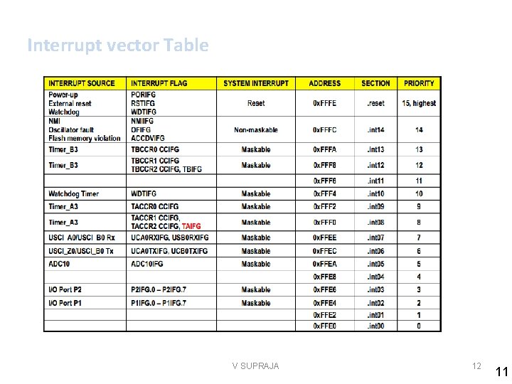
Interrupt vector Table V SUPRAJA 12 11

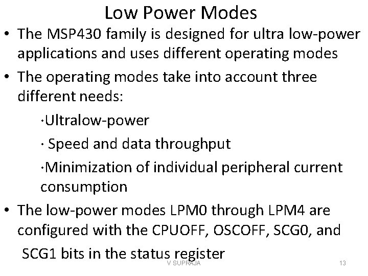
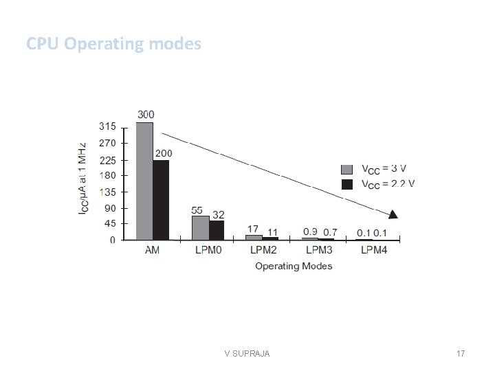
Low Power Modes • The MSP 430 family is designed for ultra low-power applications and uses different operating modes • The operating modes take into account three different needs: ·Ultralow-power · Speed and data throughput ·Minimization of individual peripheral current consumption • The low-power modes LPM 0 through LPM 4 are configured with the CPUOFF, OSCOFF, SCG 0, and SCG 1 bits in the status register V SUPRAJA 13

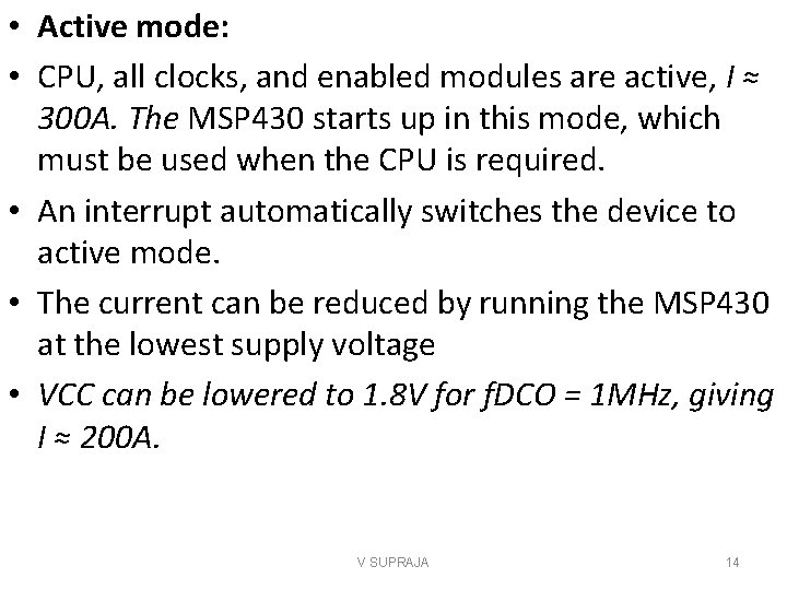
• Active mode: • CPU, all clocks, and enabled modules are active, I ≈ 300 A. The MSP 430 starts up in this mode, which must be used when the CPU is required. • An interrupt automatically switches the device to active mode. • The current can be reduced by running the MSP 430 at the lowest supply voltage • VCC can be lowered to 1. 8 V for f. DCO = 1 MHz, giving I ≈ 200 A. V SUPRAJA 14

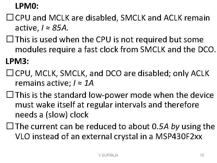
LPM 0: � CPU and MCLK are disabled, SMCLK and ACLK remain active, I ≈ 85 A. � This is used when the CPU is not required but some modules require a fast clock from SMCLK and the DCO. LPM 3: � CPU, MCLK, SMCLK, and DCO are disabled; only ACLK remains active; I ≈ 1 A � This is the standard low-power mode when the device must wake itself at regular intervals and therefore needs a (slow) clock � The current can be reduced to about 0. 5 A by using the VLO instead of an external crystal in a MSP 430 F 2 xx V SUPRAJA 15

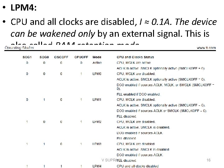
• LPM 4: • CPU and all clocks are disabled, I ≈ 0. 1 A. The device can be wakened only by an external signal. This is also called RAM retention mode. V SUPRAJA 16

CPU Operating modes V SUPRAJA 17

Waking from a Low power mode • An interrupt is needed to awaken the MSP 430. The processor handles an interrupt from a low-power mode in almost the same way as in active mode • Status register is cleared when an interrupt is accepted, which puts the processor into active mode • MCLK is automatically turned off at the end of the ISR if the MSP 430 returns to a low-power mode when the status register is restored. V SUPRAJA 18

• Sometimes it is not appropriate to carry out all actions in an ISR and it is better to return to the main function in active mode • In this case we must clear all the low-power bits in the saved value of SR on the stack before it is restored at the end of the interrupt service routine. V SUPRAJA 19

Entering and Exiting Low-Power Modes • Enter interrupt service routine: – The PC and SR are stored on the stack – The CPUOFF, SCG 1, and OSCOFF bits are automatically reset • Options for returning from the interrupt service routine: – The original SR is popped from the stack, restoring the previous operating mode. – The SR bits stored on the stack can be modified within the interrupt service routine V SUPRAJA 20

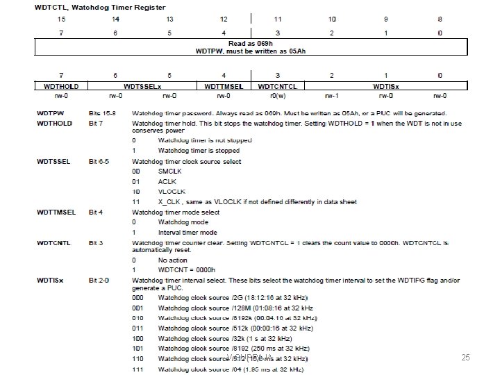
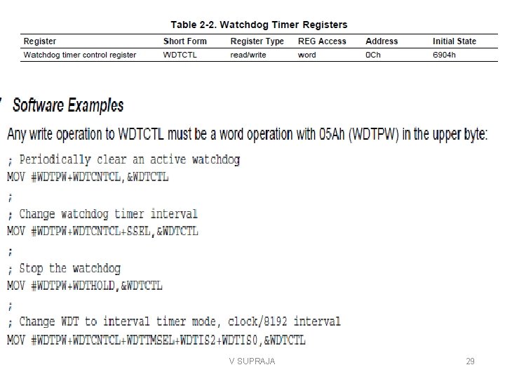
Watchdog Timer • The main purpose of the watchdog timer is to protect the system against failure of the software, such as the program becoming trapped in an unintended, infinite loop. • If the selected time interval expires, a system reset is generated. • The operation of the watchdog is controlled by the 16 -bit register WDTCTL V SUPRAJA 21

• Features of the watchdog timer module include: · Eight software-selectable time intervals · Watchdog mode · Interval mode · Access to WDT control register is password protected · Selectable clock source · Can be stopped to conserve power · Clock fail-safe feature V SUPRAJA 22

V SUPRAJA 23

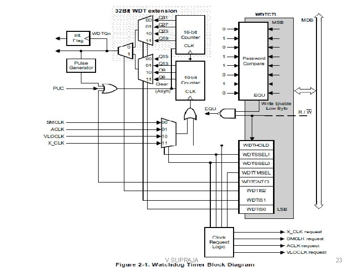
• The WDT module can be configured as either a watchdog or interval timer with the WDTCTL register. • WDTCTL is a 16 -bit, password-protected, read/write register • write accesses must include the write password 05 Ah in the upper byte • Any read of WDTCTL reads 069 h in the upper byte. • The watchdog timer counter (WDTCNT) is a 32 -bit up-counter that is not directly accessible by software • The WDTCNT can be sourced from SMCLK, ACLK, VLOCLK and X_CLK on some devices. The clock source is selected with the WDTSSEL bits V SUPRAJA 24

V SUPRAJA 25

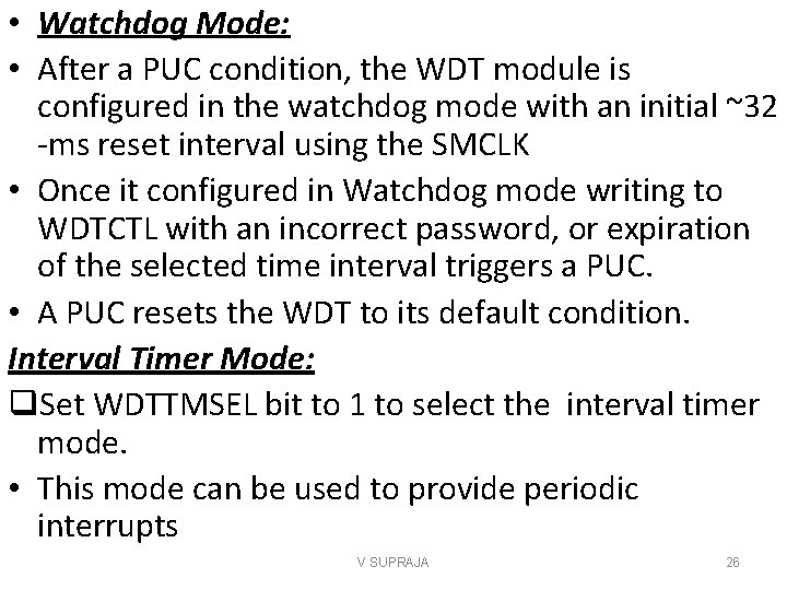
• Watchdog Mode: • After a PUC condition, the WDT module is configured in the watchdog mode with an initial ~32 -ms reset interval using the SMCLK • Once it configured in Watchdog mode writing to WDTCTL with an incorrect password, or expiration of the selected time interval triggers a PUC. • A PUC resets the WDT to its default condition. Interval Timer Mode: q. Set WDTTMSEL bit to 1 to select the interval timer mode. • This mode can be used to provide periodic interrupts V SUPRAJA 26

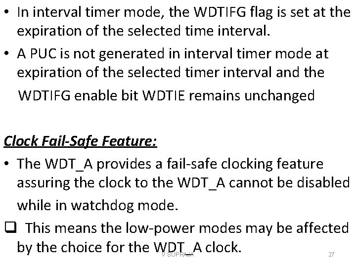
• In interval timer mode, the WDTIFG flag is set at the expiration of the selected time interval. • A PUC is not generated in interval timer mode at expiration of the selected timer interval and the WDTIFG enable bit WDTIE remains unchanged Clock Fail-Safe Feature: • The WDT_A provides a fail-safe clocking feature assuring the clock to the WDT_A cannot be disabled while in watchdog mode. q This means the low-power modes may be affected by the choice for the WDT_A clock. V SUPRAJA 27

• If SMCLK or ACLK fails as WDT_A clock source then VLOCLK is automatically selected as WDT_A clock source. • When the WDT_A module is used in interval timer mode, there is no fail-safe feature within WDT_A for the clock source. V SUPRAJA 28

V SUPRAJA 29

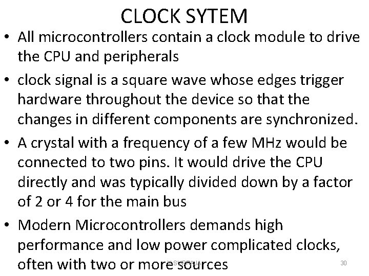
CLOCK SYTEM • All microcontrollers contain a clock module to drive the CPU and peripherals • clock signal is a square wave whose edges trigger hardware throughout the device so that the changes in different components are synchronized. • A crystal with a frequency of a few MHz would be connected to two pins. It would drive the CPU directly and was typically divided down by a factor of 2 or 4 for the main bus • Modern Microcontrollers demands high performance and low power complicated clocks, often with two or more sources V SUPRAJA 30

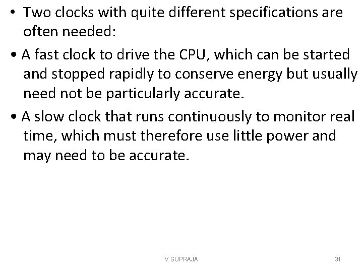
• Two clocks with quite different specifications are often needed: • A fast clock to drive the CPU, which can be started and stopped rapidly to conserve energy but usually need not be particularly accurate. • A slow clock that runs continuously to monitor real time, which must therefore use little power and may need to be accurate. V SUPRAJA 31

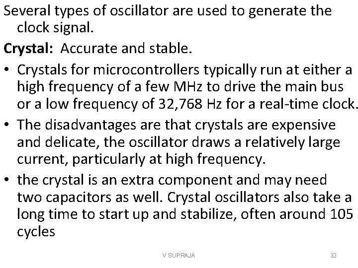
Several types of oscillator are used to generate the clock signal. Crystal: Accurate and stable. • Crystals for microcontrollers typically run at either a high frequency of a few MHz to drive the main bus or a low frequency of 32, 768 Hz for a real-time clock. • The disadvantages are that crystals are expensive and delicate, the oscillator draws a relatively large current, particularly at high frequency. • the crystal is an extra component and may need two capacitors as well. Crystal oscillators also take a long time to start up and stabilize, often around 105 cycles V SUPRAJA 32

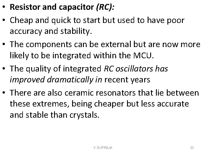
• Resistor and capacitor (RC): • Cheap and quick to start but used to have poor accuracy and stability. • The components can be external but are now more likely to be integrated within the MCU. • The quality of integrated RC oscillators has improved dramatically in recent years • There also ceramic resonators that lie between these extremes, being cheaper but less accurate and stable than crystals. V SUPRAJA 33

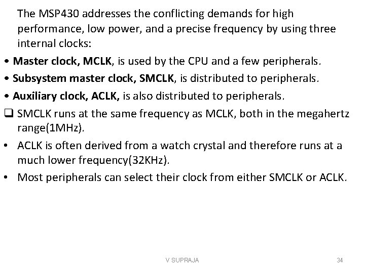
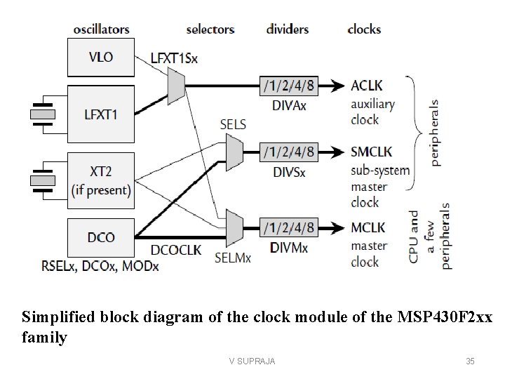
The MSP 430 addresses the conflicting demands for high performance, low power, and a precise frequency by using three internal clocks: • Master clock, MCLK, is used by the CPU and a few peripherals. • Subsystem master clock, SMCLK, is distributed to peripherals. • Auxiliary clock, ACLK, is also distributed to peripherals. q SMCLK runs at the same frequency as MCLK, both in the megahertz range(1 MHz). • ACLK is often derived from a watch crystal and therefore runs at a much lower frequency(32 KHz). • Most peripherals can select their clock from either SMCLK or ACLK. V SUPRAJA 34

Simplified block diagram of the clock module of the MSP 430 F 2 xx family V SUPRAJA 35

V SUPRAJA 36

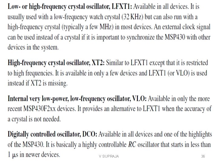
Crystal Oscillators, LFXT 1 and XT 2 • Crystals are used when an accurate, stable frequency is needed: • Accurate means that the frequency is close to what it says on the package, typically within 1 part in 105. • Stable means that does not change significantly with time or temperature. Ø Traditional crystals oscillated at frequencies of a few MHz. Ø Small microcontrollers use low frequency watch crystals with frequency 32 Kz. Ø Low frequency crystals disadvantage is they are more sensitive to temperature than high-frequency crystals. Ø A change of 10◦C in the temperature causes the frequency to fall by about 4 parts per million (ppm). V SUPRAJA 37

• Oscillator circuits are integrated into the MSP 430 and the crystal should be connected to pins XIN and XOUT. • The circuit is known as a Pierce oscillator and also requires a capacitance (10 pf) to ground from each pin. • The oscillator is designed to run at low power and this renders it susceptible to electromagnetic interference. • It is also possible to use high-frequency crystals (above 400 KHz) with LFXT 1 in most devices and some have a second oscillator XT 2, which works only at high frequencies. • The stability of crystals is reflected electrically in their high Q factor. This means that they oscillate for a long time after being excited. • The disadvantage of this is that the oscillator takes an equally long time to reach a stable state, typically around 105 cycles V SUPRAJA 38

Internal Low-Power, Low-Frequency Oscillator, VLO • The VLO is an internal RC oscillator that runs at around 12 KHz and can be used instead of LFXT 1 in some newer devices. • It saves the cost and space required for a crystal and reduces the current drawn. • LFXT 1 draws about 0. 8 A, which falls to 0. 5 A with the VLO • This is not impressive in terms of accuracy and stability • A variation of 10◦C changes the frequency by about 5%. you would not use the VLO for serious timing. • The purpose is often to wake the device periodically to check whether any inputs have changed, and accuracy is not important. V SUPRAJA 39

• ACLK is taken from LFXT 1 by default even where the VLO is present. • This means that current is wasted in LFXT 1 and that pins P 2. 6 and P 2. 7 in the F 20 xx are configured for a crystal. • It is usually a good idea to reconfigure the BCM+ to use the VLO and redirect port 2 for digital input/output. V SUPRAJA 40

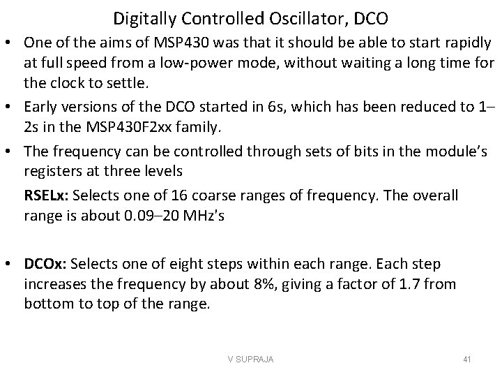
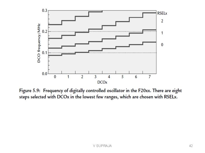
Digitally Controlled Oscillator, DCO • One of the aims of MSP 430 was that it should be able to start rapidly at full speed from a low-power mode, without waiting a long time for the clock to settle. • Early versions of the DCO started in 6 s, which has been reduced to 1– 2 s in the MSP 430 F 2 xx family. • The frequency can be controlled through sets of bits in the module’s registers at three levels RSELx: Selects one of 16 coarse ranges of frequency. The overall range is about 0. 09– 20 MHz's • DCOx: Selects one of eight steps within each range. Each step increases the frequency by about 8%, giving a factor of 1. 7 from bottom to top of the range. V SUPRAJA 41

V SUPRAJA 42

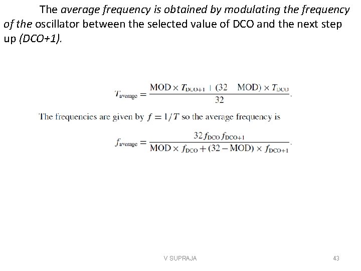
The average frequency is obtained by modulating the frequency of the oscillator between the selected value of DCO and the next step up (DCO+1). V SUPRAJA 43

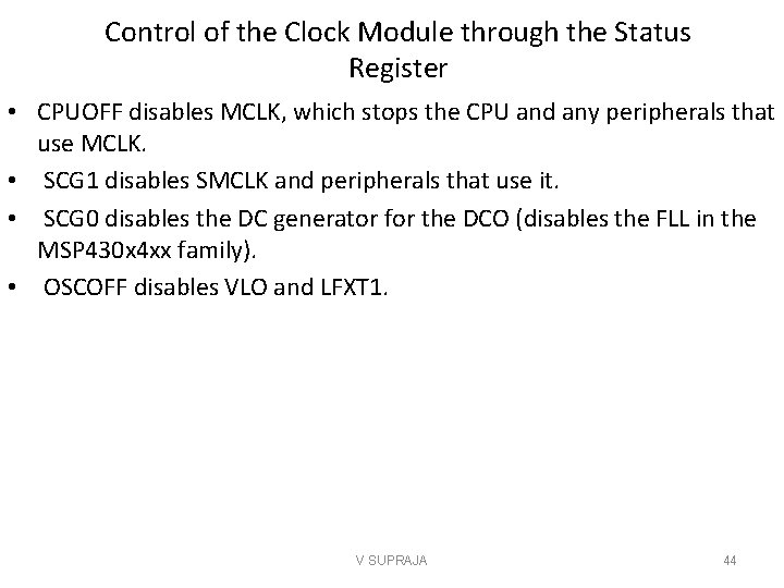
Control of the Clock Module through the Status Register • CPUOFF disables MCLK, which stops the CPU and any peripherals that use MCLK. • SCG 1 disables SMCLK and peripherals that use it. • SCG 0 disables the DC generator for the DCO (disables the FLL in the MSP 430 x 4 xx family). • OSCOFF disables VLO and LFXT 1. V SUPRAJA 44

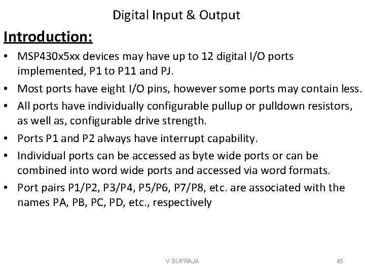
Digital Input & Output Introduction: • MSP 430 x 5 xx devices may have up to 12 digital I/O ports implemented, P 1 to P 11 and PJ. • Most ports have eight I/O pins, however some ports may contain less. • All ports have individually configurable pullup or pulldown resistors, as well as, configurable drive strength. • Ports P 1 and P 2 always have interrupt capability. • Individual ports can be accessed as byte wide ports or can be combined into word wide ports and accessed via word formats. • Port pairs P 1/P 2, P 3/P 4, P 5/P 6, P 7/P 8, etc. are associated with the names PA, PB, PC, PD, etc. , respectively V SUPRAJA 45

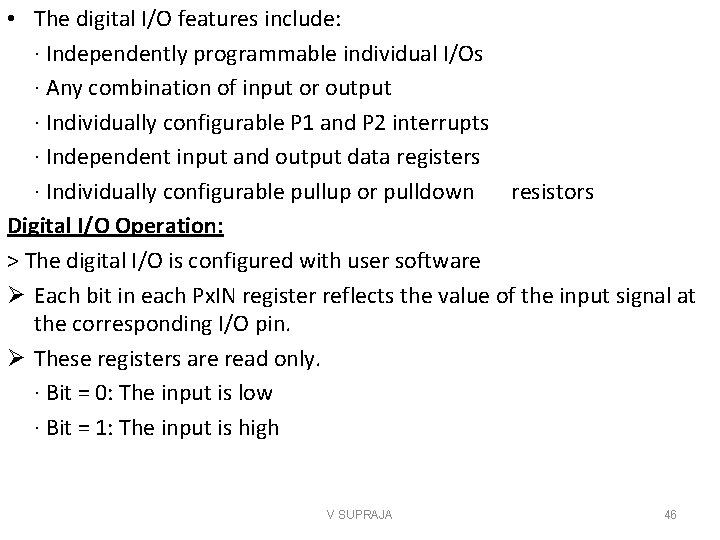
• The digital I/O features include: · Independently programmable individual I/Os · Any combination of input or output · Individually configurable P 1 and P 2 interrupts · Independent input and output data registers · Individually configurable pullup or pulldown resistors Digital I/O Operation: > The digital I/O is configured with user software Ø Each bit in each Px. IN register reflects the value of the input signal at the corresponding I/O pin. Ø These registers are read only. · Bit = 0: The input is low · Bit = 1: The input is high V SUPRAJA 46

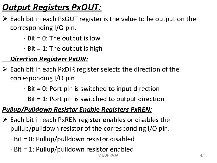
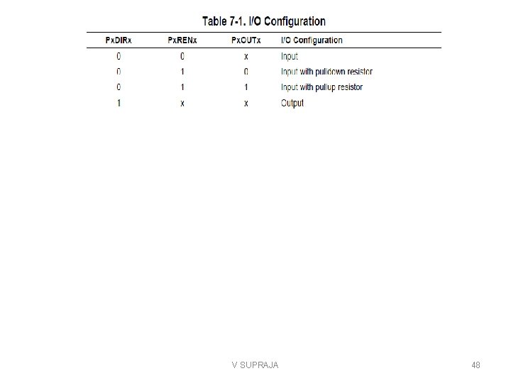
Output Registers Px. OUT: Ø Each bit in each Px. OUT register is the value to be output on the corresponding I/O pin. · Bit = 0: The output is low · Bit = 1: The output is high Direction Registers Px. DIR: Ø Each bit in each Px. DIR register selects the direction of the corresponding I/O pin · Bit = 0: Port pin is switched to input direction · Bit = 1: Port pin is switched to output direction Pullup/Pulldown Resistor Enable Registers Px. REN: Ø Each bit in each Px. REN register enables or disables the pullup/pulldown resistor of the corresponding I/O pin. · Bit = 0: Pullup/pulldown resistor disabled · Bit = 1: Pullup/pulldown resistor enabled V SUPRAJA 47

V SUPRAJA 48

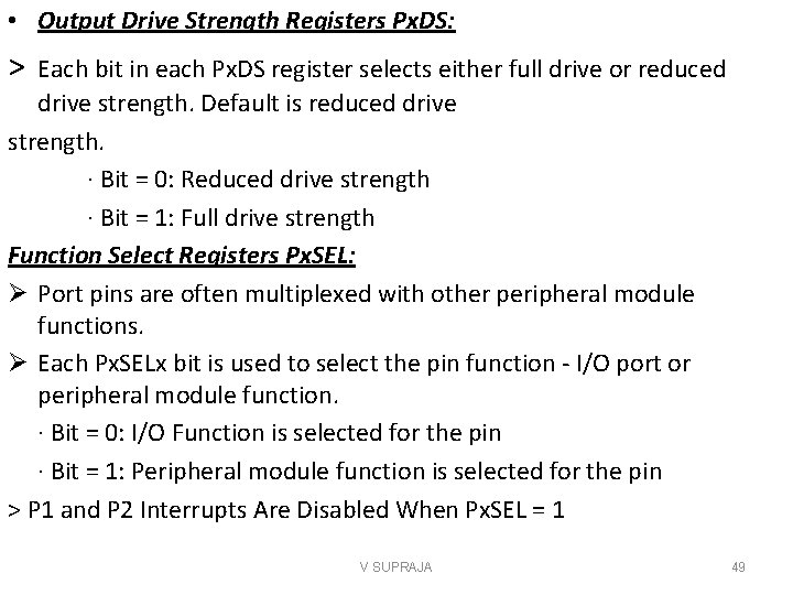
• Output Drive Strength Registers Px. DS: > Each bit in each Px. DS register selects either full drive or reduced drive strength. Default is reduced drive strength. · Bit = 0: Reduced drive strength · Bit = 1: Full drive strength Function Select Registers Px. SEL: Ø Port pins are often multiplexed with other peripheral module functions. Ø Each Px. SELx bit is used to select the pin function - I/O port or peripheral module function. · Bit = 0: I/O Function is selected for the pin · Bit = 1: Peripheral module function is selected for the pin > P 1 and P 2 Interrupts Are Disabled When Px. SEL = 1 V SUPRAJA 49

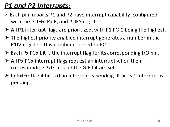
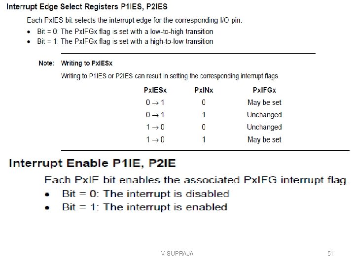
P 1 and P 2 Interrupts: > Each pin in ports P 1 and P 2 have interrupt capability, configured with the Px. IFG, Px. IE, and Px. IES registers. Ø All P 1 interrupt flags are prioritized, with P 1 IFG. 0 being the highest. Ø The highest priority enabled interrupt generates a number in the P 1 IV register. This number is added to PC. Ø Each Px. IFGx bit is the interrupt flag for its corresponding I/O pin. Ø All Px. IFGx interrupt flags request an interrupt when their corresponding Px. IE bit and the GIE bit are set. Ø In Px. IFG flag if bit is 0 no interrupt is pending. If bit is 1 interrupt is pending. V SUPRAJA 50

V SUPRAJA 51

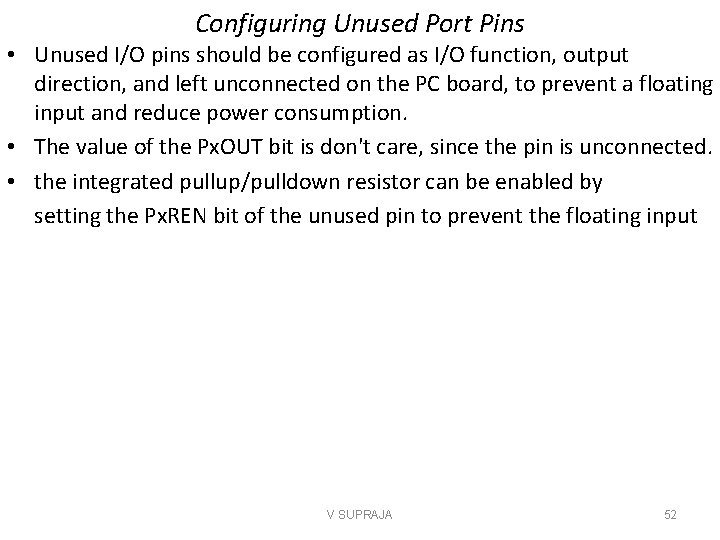
Configuring Unused Port Pins • Unused I/O pins should be configured as I/O function, output direction, and left unconnected on the PC board, to prevent a floating input and reduce power consumption. • The value of the Px. OUT bit is don't care, since the pin is unconnected. • the integrated pullup/pulldown resistor can be enabled by setting the Px. REN bit of the unused pin to prevent the floating input V SUPRAJA 52

Operating Modes • • Active Mode Low Power Mode 0(LPM 0) Low Power Mode 1(LPM 1) Low Power Mode 2(LPM 2) Low Power Mode 3(LPM 3) Low Power Mode 4(LPM 4) Low Power Mode 5(LPM 5) V SUPRAJA 53

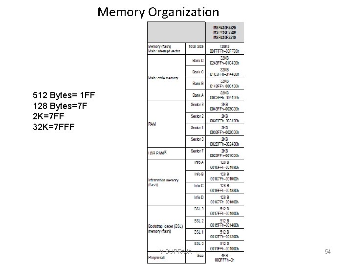
Memory Organization 512 Bytes= 1 FF 128 Bytes=7 F 2 K=7 FF 32 K=7 FFF V SUPRAJA 54

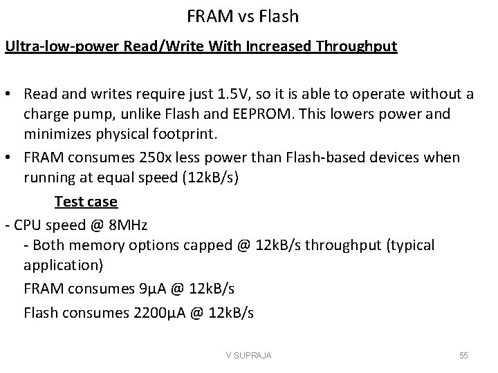
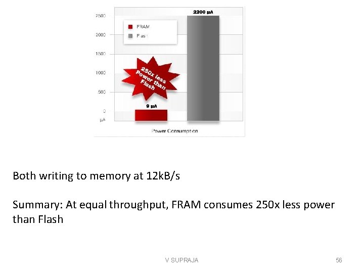
FRAM vs Flash Ultra-low-power Read/Write With Increased Throughput • Read and writes require just 1. 5 V, so it is able to operate without a charge pump, unlike Flash and EEPROM. This lowers power and minimizes physical footprint. • FRAM consumes 250 x less power than Flash-based devices when running at equal speed (12 k. B/s) Test case - CPU speed @ 8 MHz - Both memory options capped @ 12 k. B/s throughput (typical application) FRAM consumes 9μA @ 12 k. B/s Flash consumes 2200μA @ 12 k. B/s V SUPRAJA 55

Both writing to memory at 12 k. B/s Summary: At equal throughput, FRAM consumes 250 x less power than Flash V SUPRAJA 56

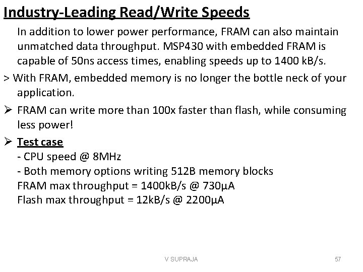
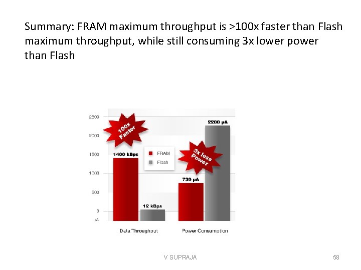
Industry-Leading Read/Write Speeds In addition to lower performance, FRAM can also maintain unmatched data throughput. MSP 430 with embedded FRAM is capable of 50 ns access times, enabling speeds up to 1400 k. B/s. > With FRAM, embedded memory is no longer the bottle neck of your application. Ø FRAM can write more than 100 x faster than flash, while consuming less power! Ø Test case - CPU speed @ 8 MHz - Both memory options writing 512 B memory blocks FRAM max throughput = 1400 k. B/s @ 730μA Flash max throughput = 12 k. B/s @ 2200μA V SUPRAJA 57

Summary: FRAM maximum throughput is >100 x faster than Flash maximum throughput, while still consuming 3 x lower power than Flash V SUPRAJA 58

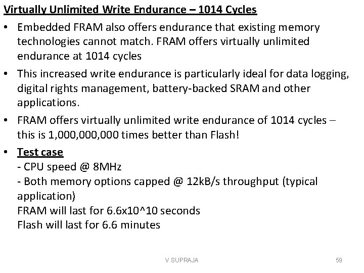
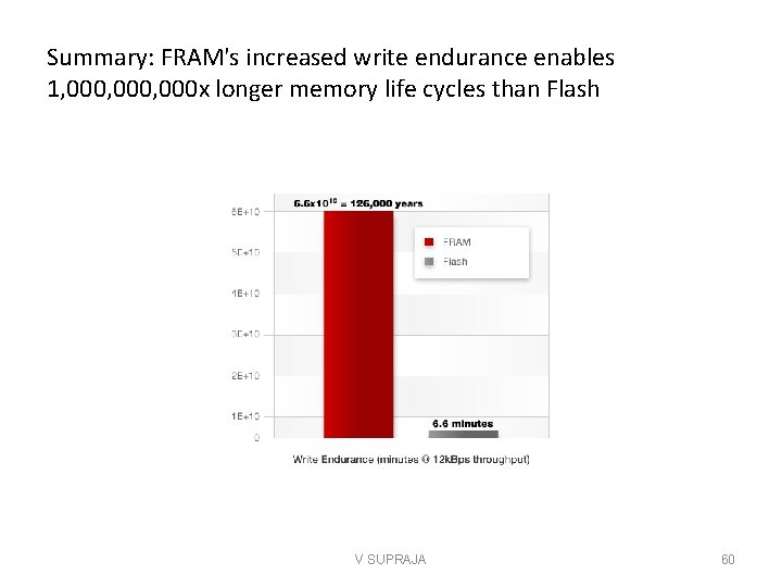
Virtually Unlimited Write Endurance – 1014 Cycles • Embedded FRAM also offers endurance that existing memory technologies cannot match. FRAM offers virtually unlimited endurance at 1014 cycles • This increased write endurance is particularly ideal for data logging, digital rights management, battery-backed SRAM and other applications. • FRAM offers virtually unlimited write endurance of 1014 cycles – this is 1, 000, 000 times better than Flash! • Test case - CPU speed @ 8 MHz - Both memory options capped @ 12 k. B/s throughput (typical application) FRAM will last for 6. 6 x 10^10 seconds Flash will last for 6. 6 minutes V SUPRAJA 59

Summary: FRAM's increased write endurance enables 1, 000, 000 x longer memory life cycles than Flash V SUPRAJA 60

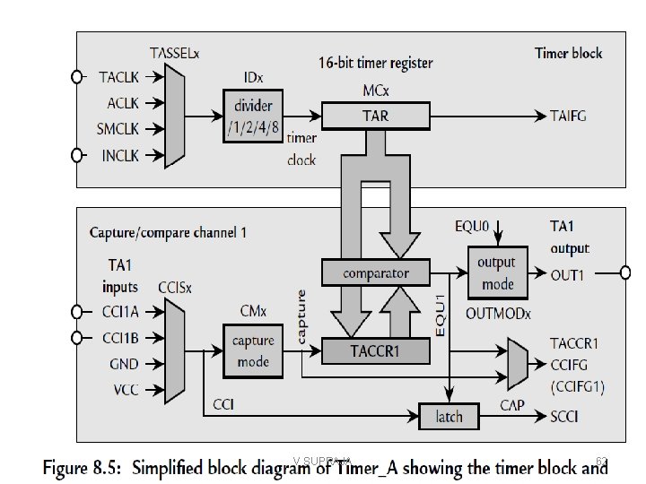
Timer_A • Timer_A is a 16 -bit timer/counter with up to seven capture/compare registers. • Timer_A can support multiple capture/compares, PWM outputs, and interval timing. • Timer_A also has extensive interrupt capabilities. V SUPRAJA 61

V SUPRAJA 62

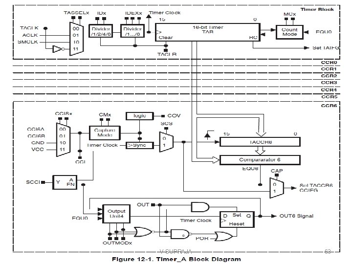
V SUPRAJA 63

Timer_A Operation • The Timer_A module is configured with user software • 16 -Bit Timer Counter: • The 16 -bit timer/counter register, TAR, increments or decrements (depending on mode of operation) with each rising edge of the clock signal. • TAR can be read or written with software. Additionally, the timer can generate an interrupt when it overflows. • TAR may be cleared by setting the TACLR bit. Setting TACLR also clears the clock divider and count direction for up/down mode. V SUPRAJA 64

• Clock Source Select and Divider: • The timer clock TACLK can be sourced from ACLK, SMCLK, or externally via TACLK. • The clock source is selected with the TASSELx bits. The selected clock source may be passed directly to the timer or divided by 2, 4, or 8, using the IDx bits. • The selected clock source can be further divided by 2, 3, 4, 5, 6, 7, or 8 using the IDEXx bits. The TACLK dividers are reset when TACLR is set. • Starting the Timer • The timer may be started, or restarted in the following ways: · The timer counts when MCx > 0 and the clock source is active. · When the timer mode is either up or up/down, the timer may be stopped by writing 0 to TACCR 0. V SUPRAJA 65

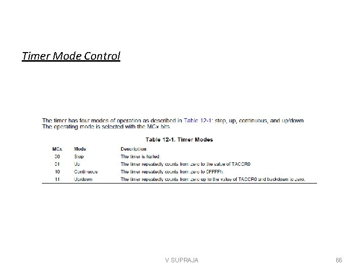
Timer Mode Control V SUPRAJA 66

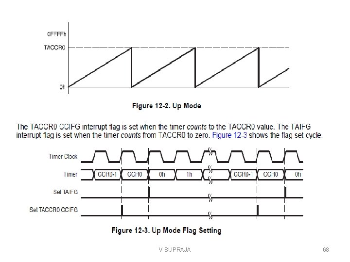
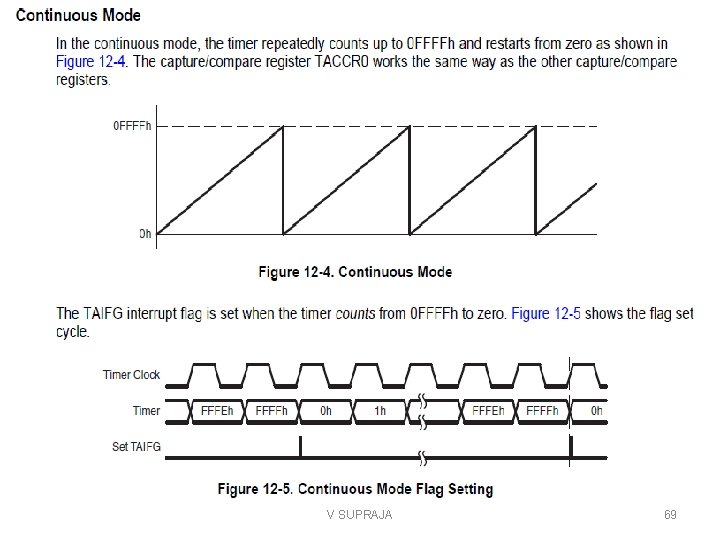
Up Mode • The up mode is used if the timer period must be different from 0 FFFFh counts. • When the timer value equals TACCR 0 the timer restarts counting from zero • Changing the Period Register TACCR 0 • When changing TACCR 0 while the timer is running, if the new period is greater than or equal to the old period, or greater than the current count value, the timer counts up to the new period. • If the new period is less than the current count value, the timer rolls to zero V SUPRAJA 67

V SUPRAJA 68

V SUPRAJA 69

• Use of the Continuous Mode • The continuous mode can be used to generate independent time intervals and output frequencies. Each time an interval is completed, an interrupt is generated. V SUPRAJA 70

V SUPRAJA 71

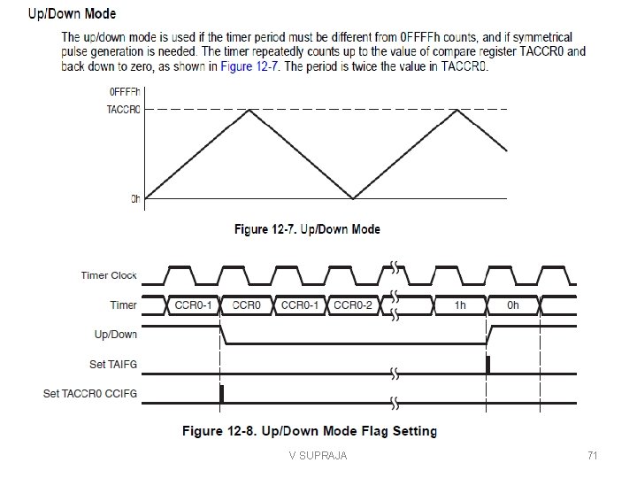
• Changing the Period Register TACCR 0 • When changing TACCR 0 while the timer is running, and counting in the down direction, the timer continues its descent until it reaches zero. The new period takes affect after the counter counts down to zero. • When the timer is counting in the up direction, and the new period is greater than or equal to the old period, or greater than the current count value, the timer counts up to the new period before counting down. • When the timer is counting in the up direction, and the new period is less than the current count value, the timer begins counting down. V SUPRAJA 72

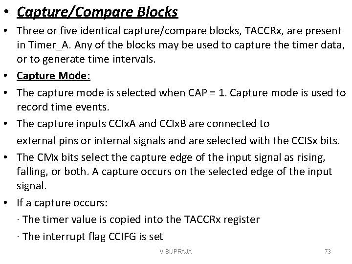
• Capture/Compare Blocks • Three or five identical capture/compare blocks, TACCRx, are present in Timer_A. Any of the blocks may be used to capture the timer data, or to generate time intervals. • Capture Mode: • The capture mode is selected when CAP = 1. Capture mode is used to record time events. • The capture inputs CCIx. A and CCIx. B are connected to external pins or internal signals and are selected with the CCISx bits. • The CMx bits select the capture edge of the input signal as rising, falling, or both. A capture occurs on the selected edge of the input signal. • If a capture occurs: · The timer value is copied into the TACCRx register · The interrupt flag CCIFG is set V SUPRAJA 73

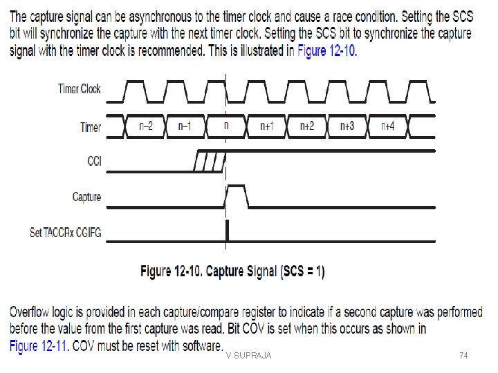
V SUPRAJA 74

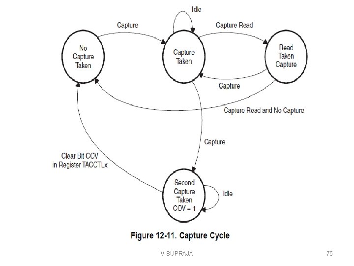
V SUPRAJA 75

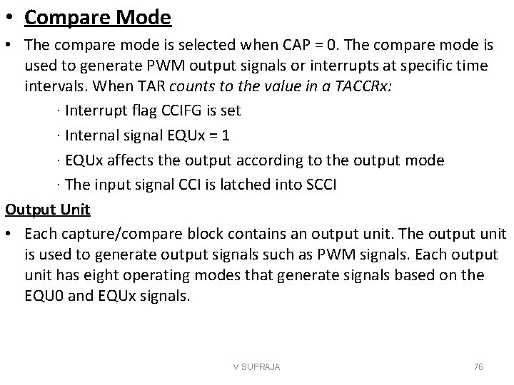
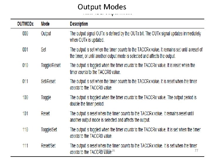
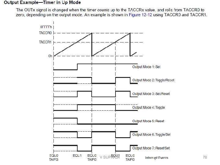
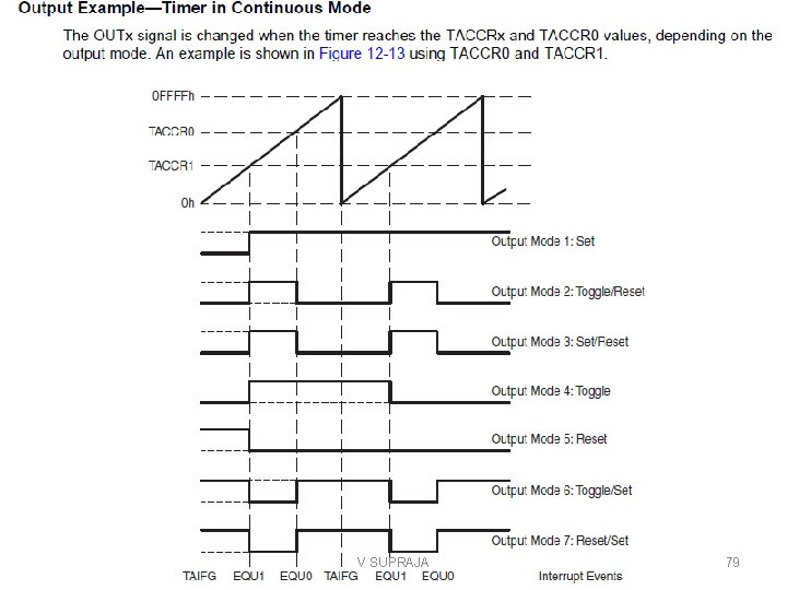
• Compare Mode • The compare mode is selected when CAP = 0. The compare mode is used to generate PWM output signals or interrupts at specific time intervals. When TAR counts to the value in a TACCRx: · Interrupt flag CCIFG is set · Internal signal EQUx = 1 · EQUx affects the output according to the output mode · The input signal CCI is latched into SCCI Output Unit • Each capture/compare block contains an output unit. The output unit is used to generate output signals such as PWM signals. Each output unit has eight operating modes that generate signals based on the EQU 0 and EQUx signals. V SUPRAJA 76

Output Modes V SUPRAJA 77

V SUPRAJA 78

V SUPRAJA 79

Timer_A Interrupts • Two interrupt vectors are associated with the 16 -bit Timer_A module: · TACCR 0 interrupt vector for TACCR 0 CCIFG · TAIV interrupt vector for all other CCIFG flags and TAIFG • In capture mode any CCIFG flag is set when a timer value is captured in the associated TACCRx register. • In compare mode, any CCIFG flag is set if TAR counts to the associated TACCRx value. V SUPRAJA 80

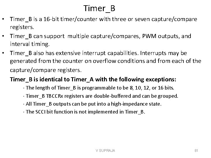
Timer_B • Timer_B is a 16 -bit timer/counter with three or seven capture/compare registers. • Timer_B can support multiple capture/compares, PWM outputs, and interval timing. • Timer_B also has extensive interrupt capabilities. Interrupts may be generated from the counter on overflow conditions and from each of the capture/compare registers. Timer_B is identical to Timer_A with the following exceptions: · The length of Timer_B is programmable to be 8, 10, 12, or 16 bits. · Timer_B TBCCRx registers are double-buffered and can be grouped. · All Timer_B outputs can be put into a high-impedance state. · The SCCI bit function is not implemented in Timer_B. V SUPRAJA 81

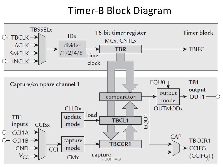
Timer-B Block Diagram V SUPRAJA 82

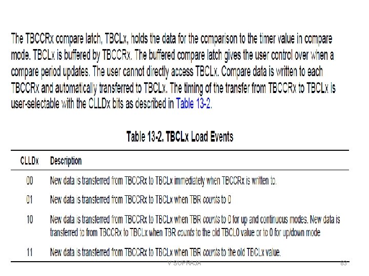
V SUPRAJA 83

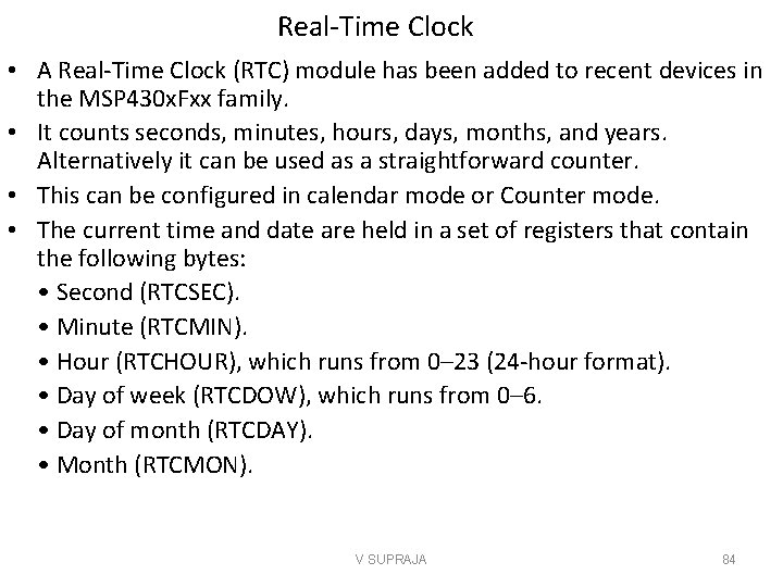
Real-Time Clock • A Real-Time Clock (RTC) module has been added to recent devices in the MSP 430 x. Fxx family. • It counts seconds, minutes, hours, days, months, and years. Alternatively it can be used as a straightforward counter. • This can be configured in calendar mode or Counter mode. • The current time and date are held in a set of registers that contain the following bytes: • Second (RTCSEC). • Minute (RTCMIN). • Hour (RTCHOUR), which runs from 0– 23 (24 -hour format). • Day of week (RTCDOW), which runs from 0– 6. • Day of month (RTCDAY). • Month (RTCMON). V SUPRAJA 84

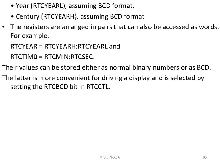
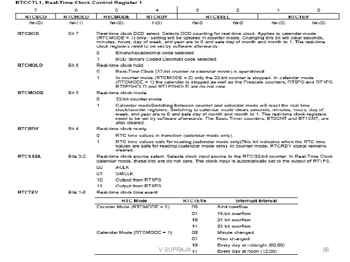
• Year (RTCYEARL), assuming BCD format. • Century (RTCYEARH), assuming BCD format • The registers are arranged in pairs that can also be accessed as words. For example, RTCYEAR = RTCYEARH: RTCYEARL and RTCTIM 0 = RTCMIN: RTCSEC. Their values can be stored either as normal binary numbers or as BCD. The latter is more convenient for driving a display and is selected by setting the RTCBCD bit in RTCCTL. V SUPRAJA 85

V SUPRAJA 86

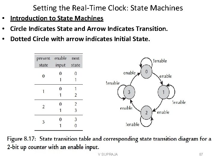
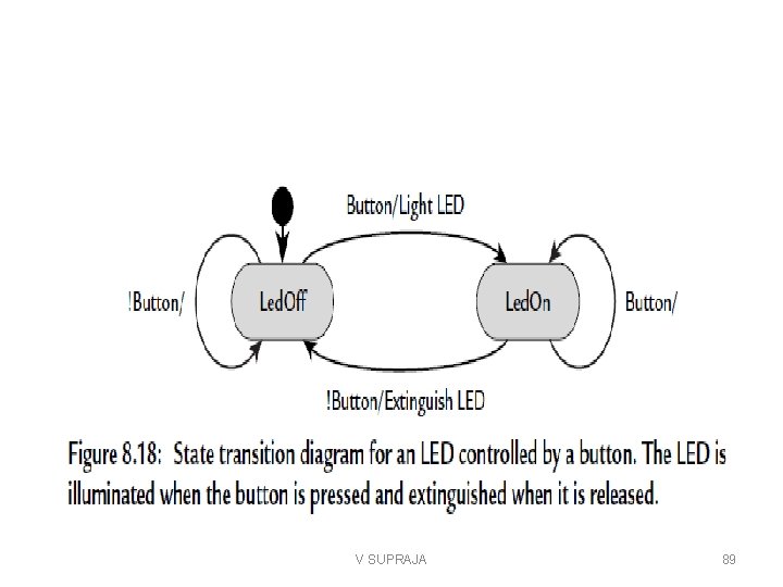
Setting the Real-Time Clock: State Machines • Introduction to State Machines • Circle Indicates State and Arrow Indicates Transition. • Dotted Circle with arrow indicates Initial State. V SUPRAJA 87

State Diagram of Read Input from a Switch • It enters the Led. Off state after initialization. The initial transition should really have an Extinguish LED action to ensure that the LED is initially switched off. • The state machine is called periodically. While the button remains up, the state machine takes the transition labeled !Button and therefore remains in the Led. Off state. • If the button is pressed when the state machine is called, it performs the Light LED action and makes a transition to the Led. On state. • The state machine remains in the Led. On state until the button is released, when it carries out the Extinguish LED action and returns to the Led. Off state. V SUPRAJA 88

V SUPRAJA 89

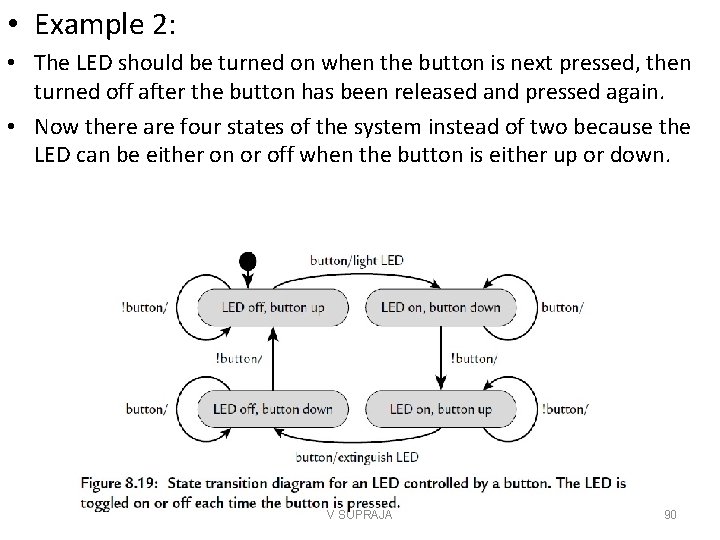
• Example 2: • The LED should be turned on when the button is next pressed, then turned off after the button has been released and pressed again. • Now there are four states of the system instead of two because the LED can be either on or off when the button is either up or down. V SUPRAJA 90

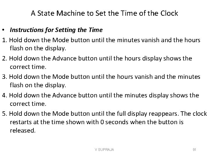
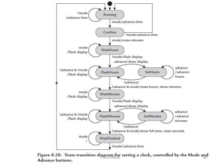
A State Machine to Set the Time of the Clock • Instructions for Setting the Time 1. Hold down the Mode button until the minutes vanish and the hours flash on the display. 2. Hold down the Advance button until the hours display shows the correct time. 3. Hold down the Mode button until the hours vanish and the minutes flash on the display. 4. Hold down the Advance button until the minutes display shows the correct time. 5. Hold down the Mode button until the full display reappears. The clock restarts at the time shown with 0 seconds when the button is released. V SUPRAJA 91

• The time should be advanced if only the Advance button is down. • The state machine should move on to the next state if only the Mode button is down. • The display should flash if neither button is down. V SUPRAJA 92

V SUPRAJA 93

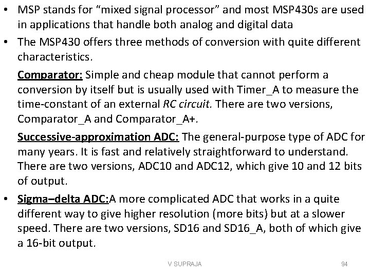
• MSP stands for “mixed signal processor” and most MSP 430 s are used in applications that handle both analog and digital data • The MSP 430 offers three methods of conversion with quite different characteristics. Comparator: Simple and cheap module that cannot perform a conversion by itself but is usually used with Timer_A to measure the time-constant of an external RC circuit. There are two versions, Comparator_A and Comparator_A+. Successive-approximation ADC: The general-purpose type of ADC for many years. It is fast and relatively straightforward to understand. There are two versions, ADC 10 and ADC 12, which give 10 and 12 bits of output. • Sigma–delta ADC: A more complicated ADC that works in a quite different way to give higher resolution (more bits) but at a slower speed. There are two versions, SD 16 and SD 16_A, both of which give a 16 -bit output. V SUPRAJA 94

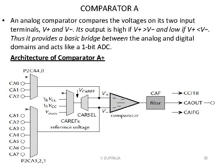
COMPARATOR A • An analog comparator compares the voltages on its two input terminals, V+ and V−. Its output is high if V+ >V− and low if V+ <V−. Thus it provides a basic bridge between the analog and digital domains and acts like a 1 -bit ADC. Architecture of Comparator A+ V SUPRAJA 95

• These are the main features of Comparator_A+. The entire module is switched on and off with the CAON bit. It is off by default to save current. • The non inverting input V+ can be connected to external signals CA 0– CA 2 or left without an external connection. This is selected using bits P 2 CA 4 and P 2 CA 0. An internal voltage reference can also be connected to V+. • Similarly, the inverting input V− can be connected to external signals CA 1–CA 7 (but not CA 0) or left unconnected, according to bits P 2 CA[3: 1]. It can also be connected to an internal reference. • The internal reference voltage VCAREF can be chosen from ¼ VCC, ½ VCC or a nominally fixed voltage from a transistor, Vdiode. This is selected with the CAREFx bits. It can be applied to either input of the comparator according to the CARSEL bit. V SUPRAJA 96

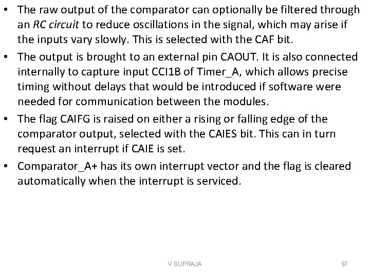
• The raw output of the comparator can optionally be filtered through an RC circuit to reduce oscillations in the signal, which may arise if the inputs vary slowly. This is selected with the CAF bit. • The output is brought to an external pin CAOUT. It is also connected internally to capture input CCI 1 B of Timer_A, which allows precise timing without delays that would be introduced if software were needed for communication between the modules. • The flag CAIFG is raised on either a rising or falling edge of the comparator output, selected with the CAIES bit. This can in turn request an interrupt if CAIE is set. • Comparator_A+ has its own interrupt vector and the flag is cleared automatically when the interrupt is serviced. V SUPRAJA 97

The ADC 10 Successive-Approximation ADC • There are two SAR ADC modules available on the MSP 430, the ADC 10 and ADC 12. • The ADC 12 has a more elaborate set of registers for storing batches of results. It needs external capacitors on its voltage reference. >Interrupts are more complicated in the ADC 12 V SUPRAJA 98

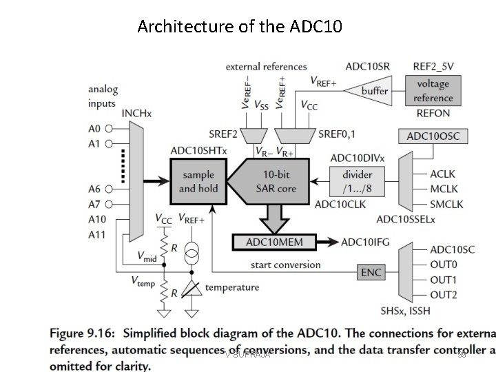
Architecture of the ADC 10 V SUPRAJA 99

• Figure shows a simplified block diagram of the ADC 10 in the F 20 x 2; there are more inputs in larger devices. • Core: • the heart of the ADC 10 is a 10 -bit, switched-capacitor, SAR core. • It is guaranteed monotonic with no missing codes. • The ADC 10 ON bit enables the core and a flag ADC 10 BUSY is set while sampling and conversion is in progress. • The result is written to ADC 10 MEM in a choice of two formats, selected with the ADC 10 DF bit: • The default is straightforward, right-justified binary in the range 0 x 0000– 0 x 03 FF. Zero corresponds to the bottom of the input range. • lowest 6 bits are always clear and bit 15 gives the sign. V SUPRAJA 100

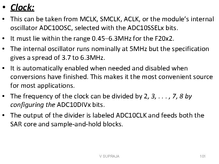
• Clock: • This can be taken from MCLK, SMCLK, ACLK, or the module’s internal oscillator ADC 10 OSC, selected with the ADC 10 SSELx bits. • It must lie within the range 0. 45– 6. 3 MHz for the F 20 x 2. • The internal oscillator runs nominally at 5 MHz but the specification gives a spread of 3. 7 to 6. 3 MHz. • It is automatically enabled when needed and disabled when conversions have finished. This makes it the most convenient source for most applications. • The frequency of the clock can be divided by 2, 3, . . . , 7, 8 by configuring the ADC 10 DIVx bits. • The output of the divider is labeled ADC 10 CLK and feeds both the SAR core and sample-and-hold blocks. V SUPRAJA 101

• Sample and Hold: • a sample and hold (S/H, also "follow-and-hold") circuit is an analog device that samples (captures, grabs) the voltage of a continuously varying analog signal and holds (locks, freezes) its value at a constant level for a specified minimum period of time. V SUPRAJA 102

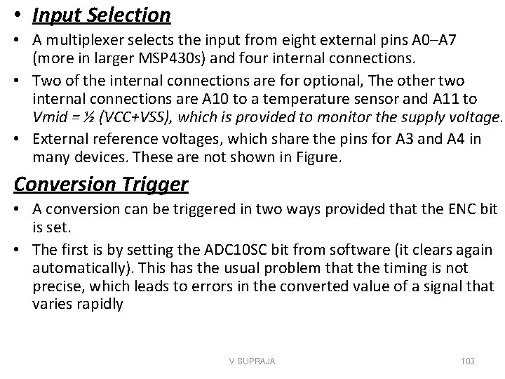
• Input Selection • A multiplexer selects the input from eight external pins A 0–A 7 (more in larger MSP 430 s) and four internal connections. • Two of the internal connections are for optional, The other two internal connections are A 10 to a temperature sensor and A 11 to Vmid = ½ (VCC+VSS), which is provided to monitor the supply voltage. • External reference voltages, which share the pins for A 3 and A 4 in many devices. These are not shown in Figure. Conversion Trigger • A conversion can be triggered in two ways provided that the ENC bit is set. • The first is by setting the ADC 10 SC bit from software (it clears again automatically). This has the usual problem that the timing is not precise, which leads to errors in the converted value of a signal that varies rapidly V SUPRAJA 103

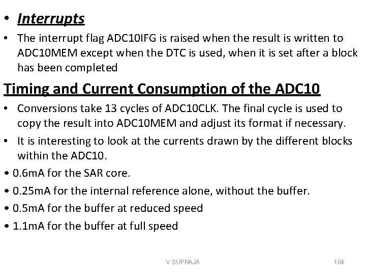
• Interrupts • The interrupt flag ADC 10 IFG is raised when the result is written to ADC 10 MEM except when the DTC is used, when it is set after a block has been completed Timing and Current Consumption of the ADC 10 • Conversions take 13 cycles of ADC 10 CLK. The final cycle is used to copy the result into ADC 10 MEM and adjust its format if necessary. • It is interesting to look at the currents drawn by the different blocks within the ADC 10. • 0. 6 m. A for the SAR core. • 0. 25 m. A for the internal reference alone, without the buffer. • 0. 5 m. A for the buffer at reduced speed • 1. 1 m. A for the buffer at full speed V SUPRAJA 104

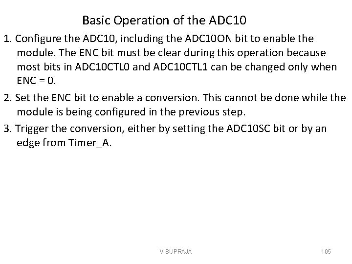
Basic Operation of the ADC 10 1. Configure the ADC 10, including the ADC 10 ON bit to enable the module. The ENC bit must be clear during this operation because most bits in ADC 10 CTL 0 and ADC 10 CTL 1 can be changed only when ENC = 0. 2. Set the ENC bit to enable a conversion. This cannot be done while the module is being configured in the previous step. 3. Trigger the conversion, either by setting the ADC 10 SC bit or by an edge from Timer_A. V SUPRAJA 105

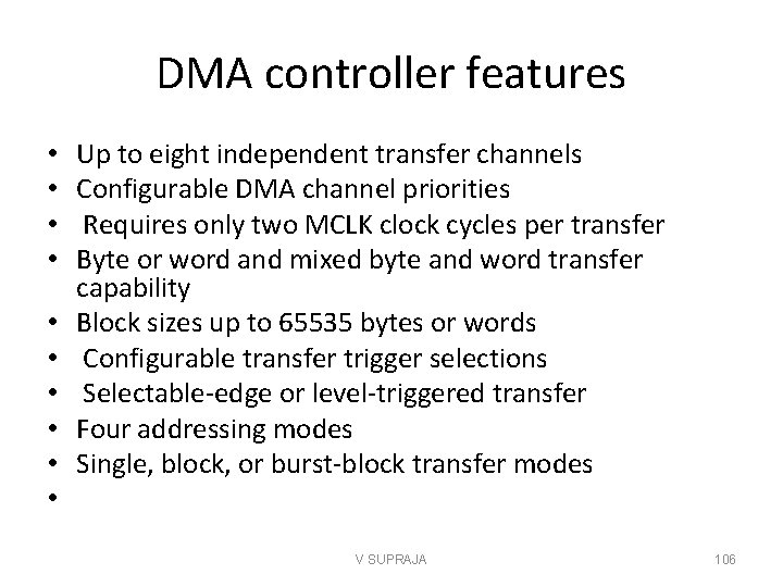
DMA controller features • • • Up to eight independent transfer channels Configurable DMA channel priorities Requires only two MCLK clock cycles per transfer Byte or word and mixed byte and word transfer capability Block sizes up to 65535 bytes or words Configurable transfer trigger selections Selectable-edge or level-triggered transfer Four addressing modes Single, block, or burst-block transfer modes V SUPRAJA 106

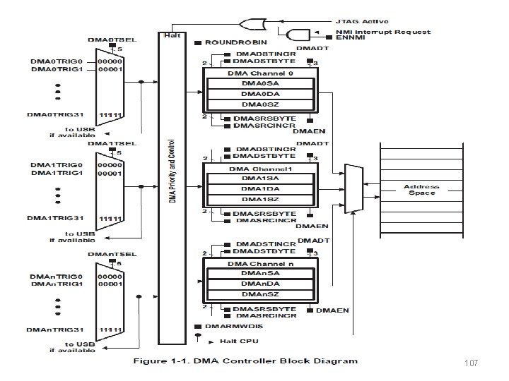
V SUPRAJA 107

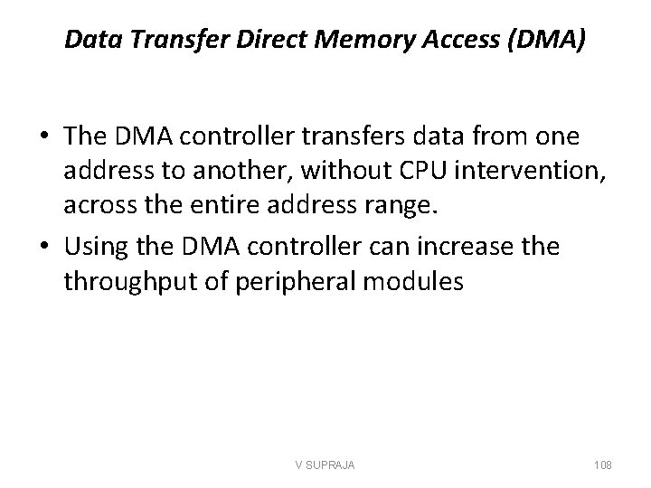
Data Transfer Direct Memory Access (DMA) • The DMA controller transfers data from one address to another, without CPU intervention, across the entire address range. • Using the DMA controller can increase throughput of peripheral modules V SUPRAJA 108

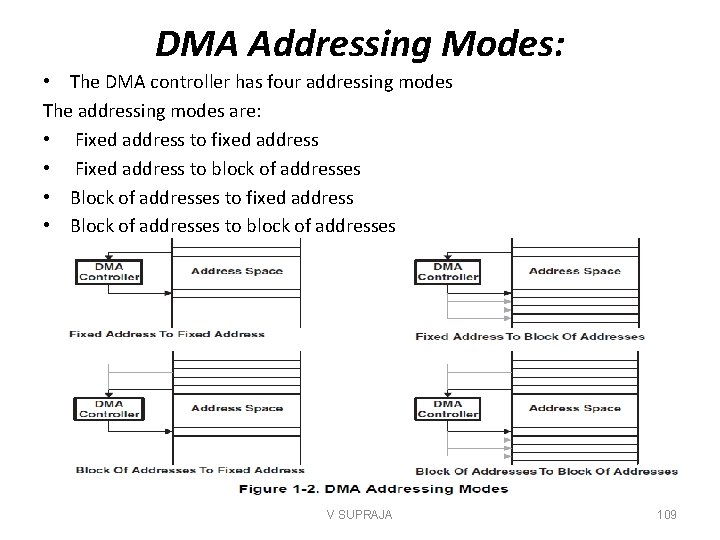
DMA Addressing Modes: • The DMA controller has four addressing modes The addressing modes are: • Fixed address to fixed address • Fixed address to block of addresses • Block of addresses to fixed address • Block of addresses to block of addresses V SUPRAJA 109

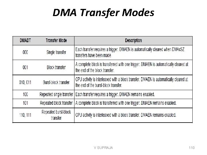
DMA Transfer Modes V SUPRAJA 110

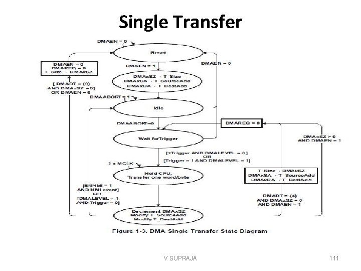
Single Transfer V SUPRAJA 111

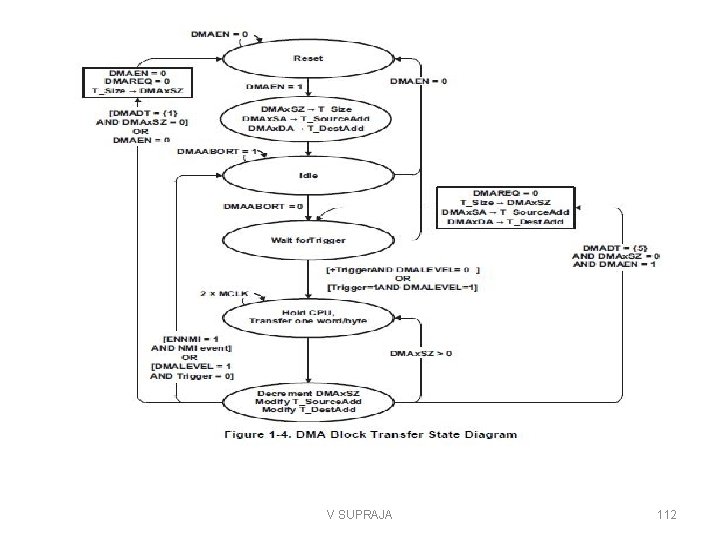
V SUPRAJA 112

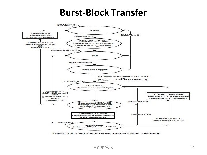
Burst-Block Transfer V SUPRAJA 113