UNIT III Microprogrammed Control Pritee Parwekar Microprogrammed Control
- Slides: 28

UNIT – III Microprogrammed Control Pritee Parwekar

Microprogrammed Control Unit • Control signals – Group of bits used to select paths in multiplexers, decoders, arithmetic logic units • Control variables – Binary variables specify microoperations • Certain microoperations initiated while others idle • Control word – String of 1’s and 0’s represent control variables Pritee Parwekar

Microprogrammed Control Unit • Control memory – Memory contains control words • Microinstructions – Control words stored in control memory – Specify control signals for execution of microoperations • Microprogram – Sequence of microinstructions Pritee Parwekar

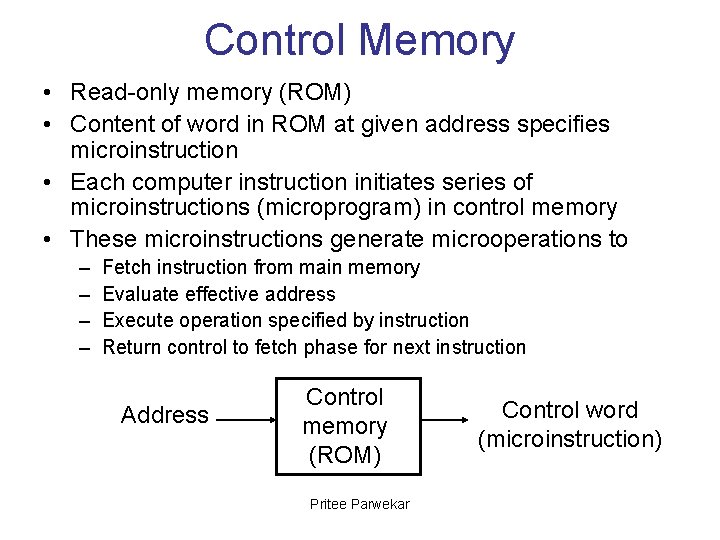
Control Memory • Read-only memory (ROM) • Content of word in ROM at given address specifies microinstruction • Each computer instruction initiates series of microinstructions (microprogram) in control memory • These microinstructions generate microoperations to – – Fetch instruction from main memory Evaluate effective address Execute operation specified by instruction Return control to fetch phase for next instruction Address Control memory (ROM) Pritee Parwekar Control word (microinstruction)

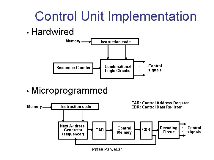
Control Unit Implementation • Hardwired Memory Instruction code Combinational Logic Circuits Sequence Counter . . Control signals • Microprogrammed Memory CAR: Control Address Register CDR: Control Data Register Instruction code Next Address Generator (sequencer) CAR Control Memory Pritee Parwekar CDR Decoding Circuit . . Control signals

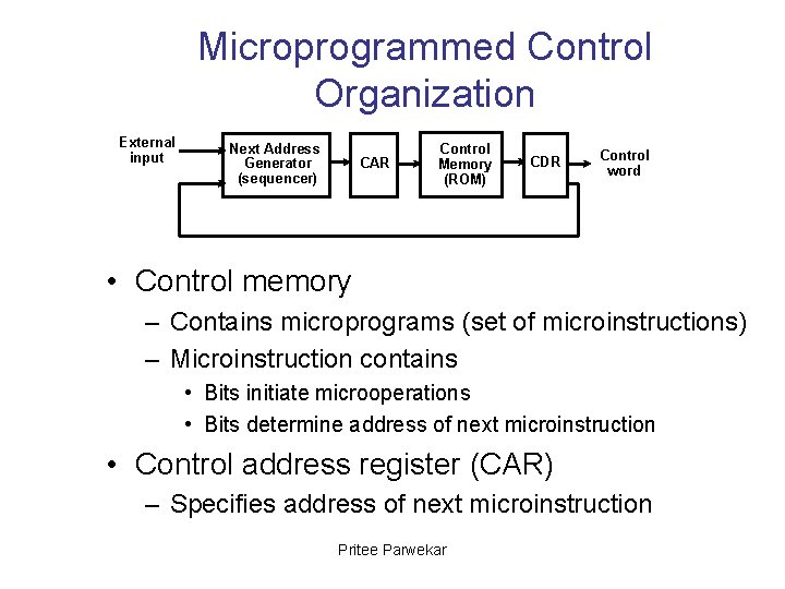
Microprogrammed Control Organization External input Next Address Generator (sequencer) CAR Control Memory (ROM) CDR Control word • Control memory – Contains microprograms (set of microinstructions) – Microinstruction contains • Bits initiate microoperations • Bits determine address of next microinstruction • Control address register (CAR) – Specifies address of next microinstruction Pritee Parwekar

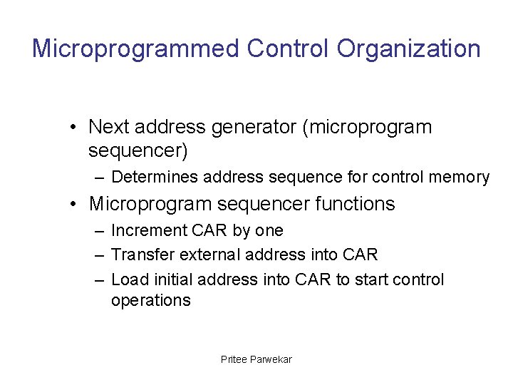
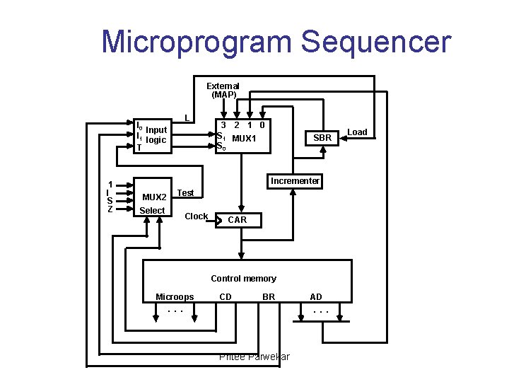
Microprogrammed Control Organization • Next address generator (microprogram sequencer) – Determines address sequence for control memory • Microprogram sequencer functions – Increment CAR by one – Transfer external address into CAR – Load initial address into CAR to start control operations Pritee Parwekar

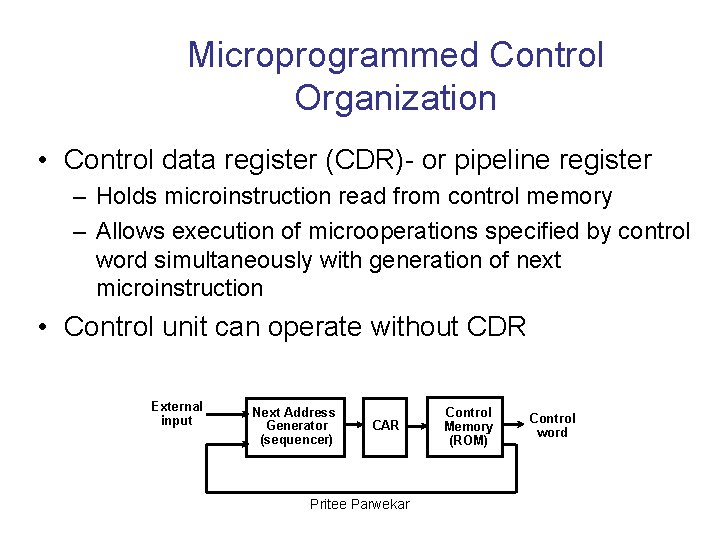
Microprogrammed Control Organization • Control data register (CDR)- or pipeline register – Holds microinstruction read from control memory – Allows execution of microoperations specified by control word simultaneously with generation of next microinstruction • Control unit can operate without CDR External input Next Address Generator (sequencer) CAR Pritee Parwekar Control Memory (ROM) Control word

Microprogram Routines • Routine – Group of microinstructions stored in control memory • Each computer instruction has its own microprogram routine to generate microoperations that execute the instruction Pritee Parwekar

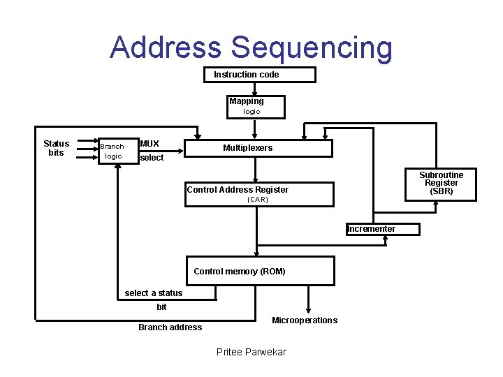
Microprogram Routines • Subroutine – Sequence of microinstructions used by other routines to accomplish particular task • Example – Subroutine to generate effective address of operand for memory reference instruction • Subroutine register (SBR) – Stores return address during subroutine call Pritee Parwekar

Conditional Branching • Branching from one routine to another depends on status bit conditions • Status bits provide parameter info such as – Carry-out of adder – Sign bit of number – Mode bits of instruction • Info in status bits can be tested and actions initiated based on their conditions: 1 or 0 • Unconditional branch – Fix value of status bit to 1 Pritee Parwekar

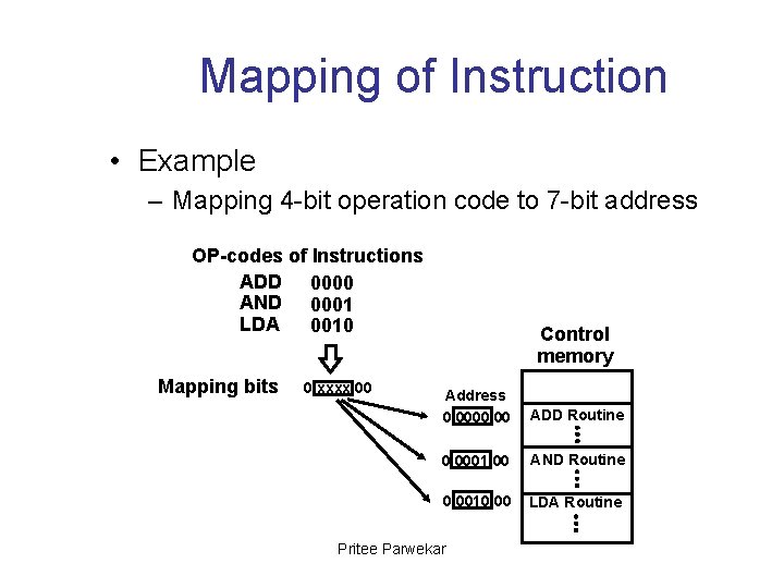
Mapping of Instruction • Each computer instruction has its own microprogram routine stored in a given location of the control memory • Mapping – Transformation from instruction code bits to address in control memory where routine is located Pritee Parwekar

Mapping of Instruction • Example – Mapping 4 -bit operation code to 7 -bit address OP-codes of Instructions ADD 0000 AND 0001 LDA 0010 Mapping bits 0 xxxx 00 Control memory Address 0 0000 00 ADD Routine 0 0001 00 AND Routine 0 0010 00 LDA Routine Pritee Parwekar

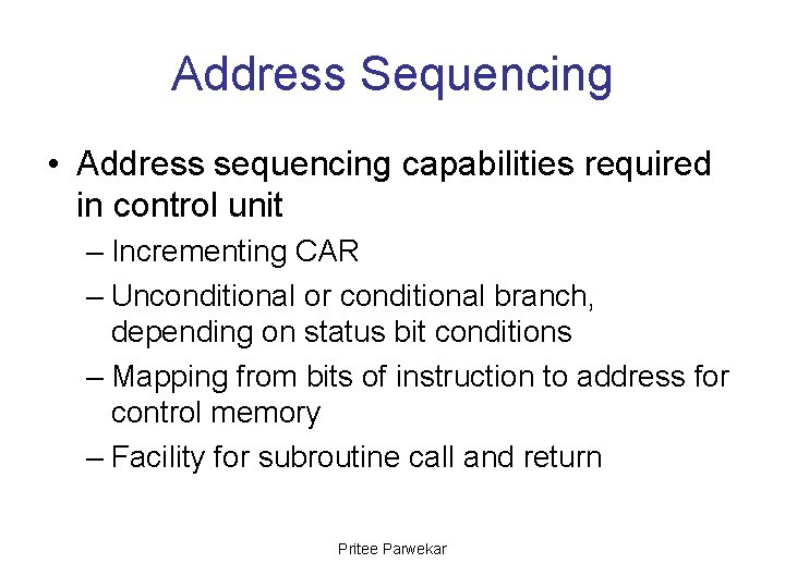
Address Sequencing • Address sequencing capabilities required in control unit – Incrementing CAR – Unconditional or conditional branch, depending on status bit conditions – Mapping from bits of instruction to address for control memory – Facility for subroutine call and return Pritee Parwekar

Address Sequencing Instruction code Mapping logic Status bits Branch logic MUX Multiplexers select Subroutine Register (SBR) Control Address Register (CAR) Incrementer Control memory (ROM) select a status bit Branch address Microoperations Pritee Parwekar

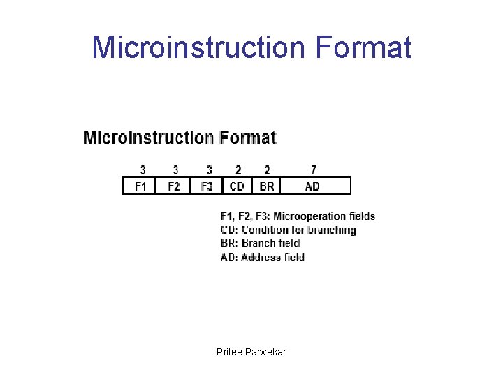
Microinstruction Format Pritee Parwekar

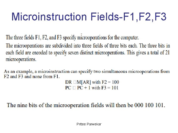
Microinstruction Fields-F 1, F 2, F 3 Pritee Parwekar

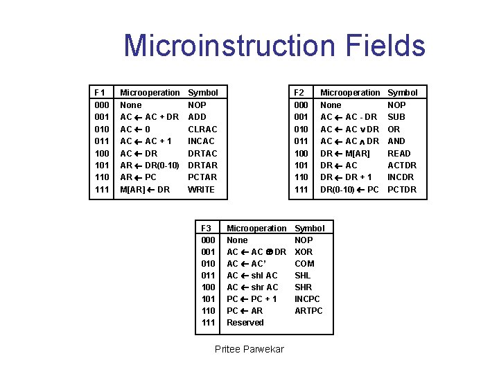
Microinstruction Fields F 1 000 001 010 011 100 101 110 111 Microoperation None AC + DR AC 0 AC + 1 AC DR AR DR(0 -10) AR PC M[AR] DR Symbol NOP ADD CLRAC INCAC DRTAR PCTAR WRITE F 3 000 001 010 011 100 101 110 111 F 2 000 001 010 011 100 101 110 111 Microoperation None AC DR AC AC’ AC shl AC AC shr AC PC + 1 PC AR Reserved Pritee Parwekar Microoperation None AC - DR AC AC DR DR M[AR] DR AC DR + 1 DR(0 -10) PC Symbol NOP XOR COM SHL SHR INCPC ARTPC Symbol NOP SUB OR AND READ ACTDR INCDR PCTDR

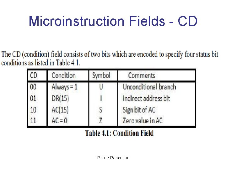
Microinstruction Fields - CD Pritee Parwekar

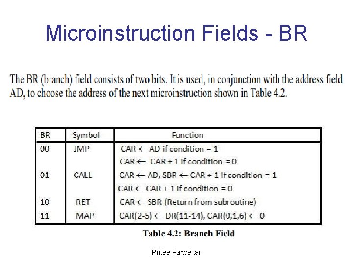
Microinstruction Fields - BR Pritee Parwekar

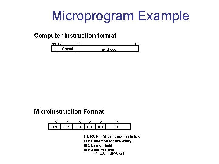
Microprogram Example Computer instruction format 15 14 11 10 Opcode I 0 Address Microinstruction Format 3 F 1 3 F 2 3 F 3 2 CD 2 BR 7 AD F 1, F 2, F 3: Microoperation fields CD: Condition for branching BR: Branch field AD: Address field Pritee Parwekar

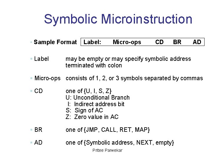
Symbolic Microinstruction § Sample Format § Label: Micro-ops CD BR AD may be empty or may specify symbolic address terminated with colon § Micro-ops consists of 1, 2, or 3 symbols separated by commas § CD one of {U, I, S, Z} U: Unconditional Branch I: Indirect address bit S: Sign of AC Z: Zero value in AC § BR one of {JMP, CALL, RET, MAP} § AD one of {Symbolic address, NEXT, empty} Pritee Parwekar

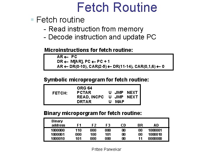
Fetch Routine § Fetch routine - Read instruction from memory - Decode instruction and update PC Microinstructions for fetch routine: AR PC DR M[AR], PC + 1 AR DR(0 -10), CAR(2 -5) DR(11 -14), CAR(0, 1, 6) 0 Symbolic microprogram for fetch routine: FETCH: ORG 64 PCTAR READ, INCPC DRTAR U JMP NEXT U MAP Binary microporgram for fetch routine: Binary address 1000000 1000001 1000010 F 1 110 000 101 F 2 000 100 000 F 3 000 101 000 CD 00 00 00 Pritee Parwekar BR 00 00 11 AD 1000001 1000010 0000000

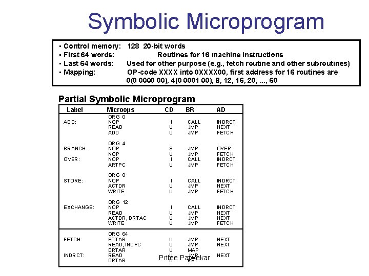
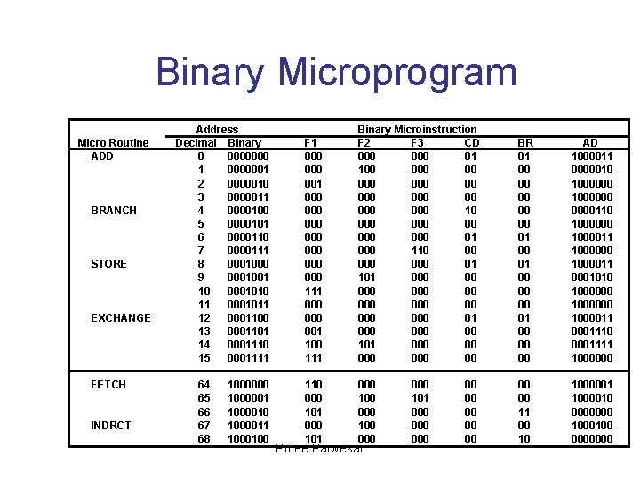
Symbolic Microprogram • Control memory: 128 20 -bit words • First 64 words: Routines for 16 machine instructions • Last 64 words: Used for other purpose (e. g. , fetch routine and other subroutines) • Mapping: OP-code XXXX into 0 XXXX 00, first address for 16 routines are 0(0 0000 00), 4(0 0001 00), 8, 12, 16, 20, . . . , 60 Partial Symbolic Microprogram Label ADD: BRANCH: OVER: STORE: EXCHANGE: FETCH: INDRCT: Microops BR AD I U U CALL JMP INDRCT NEXT FETCH ORG 4 NOP NOP ARTPC S U I U JMP CALL JMP OVER FETCH INDRCT FETCH ORG 8 NOP ACTDR WRITE I U U CALL JMP INDRCT NEXT FETCH ORG 12 NOP READ ACTDR, DRTAC WRITE I U U U CALL JMP JMP INDRCT NEXT FETCH ORG 0 NOP READ ADD ORG 64 PCTAR READ, INCPC DRTAR READ DRTAR CD U U Pritee U JMP MAP JMP Parwekar RET NEXT

Binary Microprogram Micro Routine ADD BRANCH STORE EXCHANGE FETCH INDRCT Address Decimal Binary 0 0000000 1 0000001 2 0000010 3 0000011 4 0000100 5 0000101 6 0000110 7 0000111 8 0001000 9 0001001 10 0001010 11 0001011 12 0001100 13 0001101 14 0001110 15 0001111 64 65 66 67 68 1000000 1000001 1000010 1000011 1000100 F 1 000 000 000 111 000 001 100 111 Binary Microinstruction F 2 F 3 CD 000 01 100 000 000 000 10 000 000 01 000 110 00 000 01 101 000 000 000 01 000 00 101 000 000 00 BR 01 00 00 00 01 00 00 00 AD 1000011 0000010 1000000110 1000000 1000011 0001010 1000000 100001110 0001111 1000000 110 000 101 000 100 000 00 00 11 00 10 1000001 1000010 0000000 1000100 0000000 Pritee Parwekar 000 101 000 000 00 00

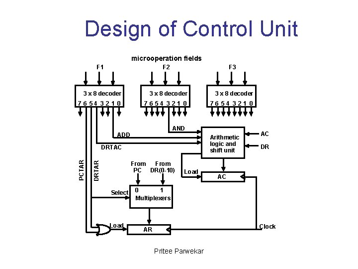
Design of Control Unit microoperation fields F 1 F 2 F 3 3 x 8 decoder 7 6 54 3 21 0 76 54 3 21 0 AND ADD Arithmetic logic and shift unit DRTAR PCTAR DRTAC From PC DR(0 -10) Select Load AC DR AC 0 1 Multiplexers Clock AR Pritee Parwekar

Microprogram Sequencer External (MAP) L I 0 Input I 1 logic T 1 I S Z 3 2 1 0 S 1 MUX 1 S 0 SBR Incrementer MUX 2 Test Select Clock CAR Control memory Microops CD BR . . . AD . . . Pritee Parwekar Load

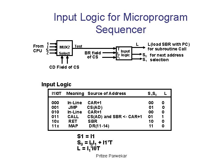
Input Logic for Microprogram Sequencer 1 From I CPU S MUX 2 Z L Test BR field of CS Select T Input I 0 logic I 1 L(load SBR with PC) for subroutine Call S 0 for next address S 1 selection CD Field of CS Input Logic I 1 I 0 T Meaning Source of Address S 1 S 0 001 010 011 10 x 11 x In-Line JMP In-Line CALL RET MAP 00 01 10 11 CAR+1 CS(AD) and SBR <- CAR+1 SBR DR(11 -14) S 1 = I 1 S 0 = I 0 I 1 + I 1’T L = I 1’I 0 T Pritee Parwekar L 0 0 0 1 0 0