UNIT III FLOORPLANNING AND PLACEMENT Contents Floor Planning


 • We often see a")
 • We need to repeat")
 : their total")
 Initial floorplan generated")
 FIGURE 16. 7 Congestion analysis. (a) The initial floorplan")


 FIGURE 16. 9 Defining the channel routing order for")
 FIGURE 16. 10 Cyclic constraints. (a) A nonslicing floorplan")
 FIGURE 16. 11 Channel definition and ordering. (a) We")
 • Every chip communicates with the outside")
 A pad-limited")
 • Special power pads are used for:")
 • If we make an electrical connection")
 • A double bond connects two pads")
 • Using a pad mapping we translate")
 FIGURE 16. 13 Bonding pads. (a) This")
 • stagger-bond arrangement using two rows of")
 FIGURE 16. 14 Gate-array I/O pads. (a)")
 • The long direction of a rectangular")
 FIGURE 16. 15 Power distribution. (a) Power")

 • FIGURE 16. 17 A clock tree. (a) Minimum")
- Slides: 35
UNIT III FLOORPLANNING AND PLACEMENT
Contents • • Floor Planning Goals and Objectives Measurement of Delay in Floor Planning Tools Channel Definition
Introduction • • • Town -Microelectronic system Buildings -ASICs town planner - System partitioning architect – Floor planning builder - Placement Electrical wiring -Routing
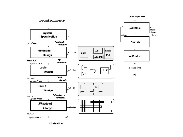
Physical Design Steps • FIGURE 15. 1 Part of an ASIC design flow showing the system partitioning, floorplanning, placement, and routing steps. These steps may be performed in a slightly different order, iterated or omitted depending on the type and size of the system and its ASICs. As the focus shifts from logic to interconnect, floorplanning assumes an increasingly important role. Each of the steps shown in the figure must be performed and each depends on the previous step. However, the trend is toward completing these steps in a parallel fashion and iterating, rather than in a sequential manner.
Introduction • • The input to the floorplanning step is the output of system partitioning and design entry—a netlist describing circuit blocks, the logic cells within the blocks, and their connections. FIGURE 16. 3 Interconnect and gate delays. As feature sizes decrease, both average interconnect delay and average gate delay decrease—but at different rates. This is because interconnect capacitance tends to a limit that is independent of scaling. Interconnect delay now dominates gate delay. Floor planning allows us to predict this interconnect delay by estimating interconnect length.
The starting point of floorplaning and placement steps for the viterbi decoder
The viterbi decoder after floorplanning and placement
Floorplanning Goals and Objectives • The input to a floorplanning tool is a hierarchical netlist that describes the interconnection of the blocks (RAM, ROM, ALU, cache controller, and so on); the logic cells (NAND, NOR, D flip-flop, and so on) within the blocks; and the logic cell connectors (the terms terminals , pins , or ports mean the same thing as connectors ). • The netlist is a logical description of the ASIC; the floorplan is a physical description of an ASIC. Floorplanning is thus a mapping between the logical description (the netlist) and the physical description (the floorplan). The goals of floorplanning are to: • arrange the blocks on a chip, • decide the location of the I/O pads, • decide the location and number of the power pads, • decide the type of power distribution, and • decide the location and type of clock distribution. The objectives of floorplanning are to minimize the chip area and minimize delay. Measuring area is straightforward, but measuring delay is more difficult and we shall explore this next.
Measurement of Delay in Floor planning Predicted –Capacitance tables-interconnect –load tables –work load tables FIGURE 16. 4 Predicted capacitance. (a) Interconnect lengths as a function of fanout (FO) and circuit-block size. (b) Wire-load table. There is only one capacitance value for each fanout (typically the average value). (c) The wire-load table predicts the capacitance and delay of a net (with a considerable error). Net A and net B both have a fanout of 1, both have the same predicted net delay, but net B in fact has a much greater delay than net A in the actual layout (of course we shall not know what the actual layout is until much later in the design process).
Measurement of Delay in Floor planning • A floorplanning tool can then use these predicted-capacitance tables (also known as interconnect-load tables or wire-load tables ). • Figure. 1 shows how we derive and use wire-load tables and illustrates the following facts: • Typically between 60 and 70 percent of nets have a FO = 1. • The distribution for a FO = 1 has a very long tail, stretching to interconnects that run from corner to corner of the chip. • The distribution for a FO = 1 often has two peaks, corresponding to a distribution for close neighbors in subgroups within a block, superimposed on a distribution corresponding to routing between subgroups.
Measurement of Delay in Floor planning (contd. , ) • We often see a twin-peaked distribution at the chip level also, corresponding to separate distributions for interblock routing (inside blocks) and intrablock routing (between blocks). • The distributions for FO > 1 are more symmetrical and flatter than for FO = 1. • The wire-load tables can only contain one number, for example the average net capacitance, for any one distribution. Many tools take a worstcase approach and use the 80 - or 90 -percentile point instead of the average. Thus a tool may use a predicted capacitance for which we know 90 percent of the nets will have less than the estimated capacitance.
Measurement of Delay in Floor planning (contd. , ) • We need to repeat the statistical analysis for blocks with different sizes. For example, a net with a FO = 1 in a 25 k-gate block will have a different (larger) average length than if the net were in a 5 k-gate block. • The statistics depend on the shape (aspect ratio) of the block (usually the statistics are only calculated for square blocks). • The statistics will also depend on the type of netlist.
Floorplanning Tools • • • Flexible blocks (or variable blocks ) : their total area is fixed, their shape (aspect ratio) and connector locations may be adjusted during the placement step. Fixed blocks: The dimensions and connector locations of the other fixed blocks (perhaps RAM, ROM, compiled cells, or megacells) can only be modified when they are created. We may force logic cells to be in selected flexible blocks by seeding. We choose seed cells by name. Seeding may be hard or soft. A hard seed is fixed and not allowed to move during the remaining floor planning and placement steps. A soft seed is an initial suggestion only and can be altered if necessary by the floor planner. We may also use seed connectors within flexible blocks—forcing certain nets to appear in a specified order, or location at the boundary of a flexible block. Rat’s nest: -display the connection between the blocks Connections are shown as bundles between the centers of blocks or as flight lines between connectors.
Floorplanning Tools • FIGURE 16. 6 Floorplanning a cell-based ASIC. (a) Initial floorplan generated by the floorplanning tool. Two of the blocks are flexible (A and C) and contain rows of standard cells (unplaced). A pop -up window shows the status of block A. (b) An estimated placement for flexible blocks A and C. The connector positions are known and a rat’s nest display shows the heavy congestion below block B. (c) Moving blocks to improve the floorplan. (d) The updated display shows the reduced congestion after the changes.
Floorplanning Tools (contd. , ) FIGURE 16. 7 Congestion analysis. (a) The initial floorplan with a 2: 1. 5 die aspect ratio. (b) Altering the floorplan to give a 1: 1 chip aspect ratio. (c) A trial floorplan with a congestion map. Blocks A and C have been placed so that we know the terminal positions in the channels. Shading indicates the ratio of channel density to the channel capacity. Dark areas show regions that cannot be routed because the channel congestion exceeds the estimated capacity. (d) Resizing flexible blocks A and C alleviates congestion.
Channel Allocation or Channel Definition • During the floorplanning step we assign the areas between blocks that are to be used for interconnect. This process is known as Channel Definition or Channel Allocation
Channel Definition FIGURE 16. 8 Routing a T-junction between two channels in two-level metal. The dots represent logic cell pins. (a) Routing channel A (the stem of the T) first allows us to adjust the width of channel B. (b) If we route channel B first (the top of the T), this fixes the width of channel A. We have to route the stem of a T-junction before we route the top.
Channel Ordering • The general problem of choosing the order of rectangular channels to route is Channel ordering.
Channel Definition (contd. , ) FIGURE 16. 9 Defining the channel routing order for a slicing floorplan using a slicing tree. (a) Make a cut all the way across the chip between circuit blocks. Continue slicing until each piece contains just one circuit block. Each cut divides a piece into two without cutting through a circuit block. (b) A sequence of cuts: 1, 2, 3, and 4 that successively slices the chip until only circuit blocks are left. (c) The slicing tree corresponding to the sequence of cuts gives the order in which to route the channels: 4, 3, 2, and finally 1.
Channel Definition (contd. , ) FIGURE 16. 10 Cyclic constraints. (a) A nonslicing floorplan with a cyclic constraint that prevents channel routing. (b) In this case it is difficult to find a slicing floorplan without increasing the chip area. (c) This floorplan may be sliced (with initial cuts 1 or 2) and has no cyclic constraints, but it is inefficient in area use and will be very difficult to route.
Channel Definition (contd. , ) FIGURE 16. 11 Channel definition and ordering. (a) We can eliminate the cyclic constraint by merging the blocks A and C. (b) A slicing structure.
I/O and Power Planning (contd. , ) • Every chip communicates with the outside world. Signals flow onto and off the chip and we need to supply power. We need to consider the I/O and power constraints early in the floorplanning process. • A silicon chip or die (plural die, dies, or dice) is mounted on a chip carrier inside a chip package. Connections are made by bonding the chip pads to fingers on a metal lead frame that is part of the package. T • The metal lead-frame fingers connect to the package pins. A die consists of a logic core inside a pad ring. • On a pad-limited die we use tall, thin pad-limited pads , which maximize the number of pads we can fit around the outside of the chip. • On a core-limited die we use short, wide core-limited pads.
I/O and Power Planning FIGURE 16. 12 Pad-limited and core-limited die. (a) A pad-limited die. The number of pads determines the die size. (b) A core-limited die: The core logic determines the die size. (c) Using both pad-limited pads and core-limited pads for a square die.
I/O and Power Planning (contd. , ) • Special power pads are used for: 1. positive supply, or VDD, power buses (or power rails ) and 2. ground or negative supply, VSS or GND. • one set of VDD/VSS pads supplies power to the I/O pads only. • Another set of VDD/VSS pads connects to a second power ring that supplies the logic core. • We sometimes call the I/O power dirty power since it has to supply large transient currents to the output transistors. We keep dirty power separate to avoid injecting noise into the internal-logic power (the clean power ). • I/O pads also contain special circuits to protect against electrostatic discharge ( ESD ). These circuits can withstand very short high-voltage (several kilovolt) pulses that can be generated during human or machine handling.
I/O and Power Planning (contd. , ) • If we make an electrical connection between the substrate and a chip pad, or to a package pin, it must be to VDD ( n -type substrate) or VSS ( p -type substrate). This substrate connection (for the whole chip) employs a down bond (or drop bond) to the carrier. We have several options: Ø We can dedicate one (or more) chip pad(s) to down bond to the chip carrier. Ø We can make a connection from a chip pad to the lead frame and down bond from the chip pad to the chip carrier. Ø We can make a connection from a chip pad to the lead frame and down bond from the lead frame. Ø We can down bond from the lead frame without using a chip pad. Ø We can leave the substrate and/or chip carrier unconnected. • Depending on the package design, the type and positioning of down bonds may be fixed. This means we need to fix the position of the chip pad for down bonding using a pad seed
I/O and Power Planning (contd. , ) • A double bond connects two pads to one chip-carrier finger and one package pin. We can do this to save package pins or reduce the series inductance of bond wires (typically a few nanohenries) by parallel connection of the pads. • To reduce the series resistive and inductive impedance of power supply networks, it is normal to use multiple VDD and VSS pads. • This is particularly important with the simultaneously switching outputs ( SSOs ) that occur when driving buses. • The output pads can easily consume most of the power on a CMOS ASIC, because the load on a pad (usually tens of picofarads) is much larger than typical on-chip capacitive loads. • Depending on the technology it may be necessary to provide dedicated VDD and VSS pads for every few SSOs. Design rules set how many SSOs can be used per VDD/VSS pad pair. These dedicated VDD/VSS pads must “follow” groups of output pads as they are seeded or planned on the floorplan.
I/O and Power Planning (contd. , ) • Using a pad mapping we translate the logical pad in a netlist to a physical pad from a pad library. We might control pad seeding and mapping in the floorplanner. • The handling of I/O pads can become quite complex; there are several nonobvious factors that must be considered when generating a pad ring: • Ideally we would only need to design library pad cells for one orientation. For example, an edge pad for the south side of the chip, and a corner pad for the southeast corner. We could then generate other orientations by rotation and flipping (mirroring). Some ASIC vendors will not allow rotation or mirroring of logic cells in the mask file. To avoid these problems we may need to have separate horizontal, vertical, left-handed, and right-handed pad cells in the library with appropriate logical to physical pad mappings. • If we mix pad-limited and core-limited edge pads in the same pad ring, this complicates the design of corner pads. Usually the two types of edge pad cannot abut. In this case a corner pad also becomes a pad-format changer , or hybrid corner pad. • In single-supply chips we have one VDD net and one VSS net, both global power nets. It is also possible to use mixed power supplies (for example, 3. 3 V and 5 V) or multiple power supplies ( digital VDD, analog VDD).
I/O and Power Planning (contd. , ) FIGURE 16. 13 Bonding pads. (a) This chip uses both pad-limited and corelimited pads. (b) A hybrid corner pad. (c) A chip with stagger-bonded pads. (d) An area-bump bonded chip (or flip-chip). The chip is turned upside down and solder bumps connect the pads to the lead frame
I/O and Power Planning (contd. , ) • stagger-bond arrangement using two rows of I/O pads. In this case the design rules for bond wires (the spacing and the angle at which the bond wires leave the pads) become very important. • Area-bump bonding arrangement (also known as flip-chip, solder-bump) used, for example, with ball-grid array ( BGA ) packages. • Even though the bonding pads are located in the center of the chip, the I/O circuits are still often located at the edges of the chip because of difficulties in power supply distribution and integrating I/O circuits together with logic in the center of the die. • In an MGA the pad spacing and I/O-cell spacing is fixed—each pad occupies a fixed pad slot (or pad site ). This means that the properties of the pad I/O are also fixed but, if we need to, we can parallel adjacent output cells to increase the drive. To increase flexibility further the I/O cells can use a separation, the I/O-cell pitch , that is smaller than the pad pitch.
I/O and Power Planning (contd. , ) FIGURE 16. 14 Gate-array I/O pads. (a) Cell-based ASICs may contain pad cells of different sizes and widths. (b) A corner of a gate-array base. (c) A gate-array base with different I/O cell and pad pitches
I/O and Power Planning (contd. , ) • The long direction of a rectangular channel is the channel spine. • Some automatic routers may require that metal lines parallel to a channel spine use a preferred layer (either m 1, m 2, or m 3). Alternatively we say that a particular metal layer runs in a preferred direction.
I/O and Power Planning (contd. , ) FIGURE 16. 15 Power distribution. (a) Power distributed using m 1 for VSS and m 2 for VDD. This helps minimize the number of vias and layer crossings needed but causes problems in the routing channels. (b) In this floorplan m 1 is run parallel to the longest side of all channels, the channel spine. This can make automatic routing easier but may increase the number of vias and layer crossings. (c) An expanded view of part of a channel (interconnect is shown as lines). If power runs on different layers along the spine of a channel, this forces signals to change layers. (d) A closeup of VDD and VSS buses as they cross. Changing layers requires a large number of via contacts to reduce
Clock Planning • clock spine routing scheme with all clock pins driven directly from the clock driver. MGAs and FPGAs often use this fish bone type of clock distribution scheme • clock skew and clock latency FIGURE 16. 16 Clock distribution. (a) A clock spine for a gate array. (b) A clock spine for a cell-based ASIC (typical chips have thousands of clock nets). (c) A clock spine is usually driven from one or more clock-driver cells. Delay in the driver cell is a function of the number of stages and the ratio of output to input capacitance for each stage (taper). (d) Clock latency and clock skew. We would like to minimize both latency and skew.
Clock Planning (cont. , ) • FIGURE 16. 17 A clock tree. (a) Minimum delay is achieved when the taper of successive stages is about 3. (b) Using a fanout of three at successive nodes. (c) A clock tree for the cell-based ASIC of Figure 16. 16 b. We have to balance the clock arrival times at all of the leaf nodes to minimize clock skew.