UNIT II Zener Diode Breakdown mechanisms applications LED
UNIT- II • Zener Diode: Breakdown mechanisms, applications, LED, LCD, Photo diode, Varactor diode, Tunnel Diode, DIAC, TRIAC, SCR, UJT , Photo transistor, IR Emitters, Solar cell, Schottky Barrier diode - Construction, operation and characteristics.
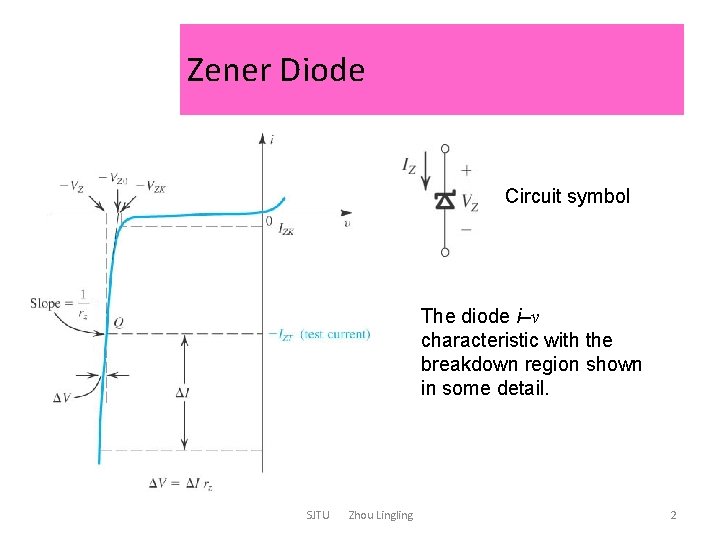
Zener Diode Circuit symbol The diode i–v characteristic with the breakdown region shown in some detail. SJTU Zhou Lingling 2
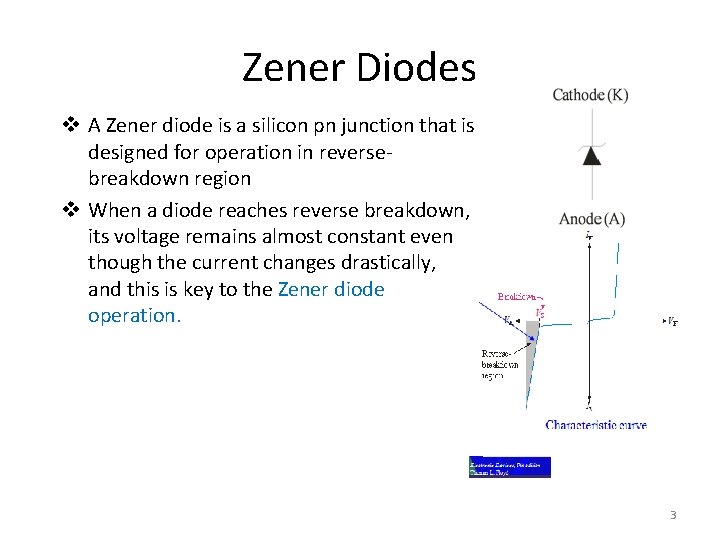
Zener Diodes v A Zener diode is a silicon pn junction that is designed for operation in reversebreakdown region v When a diode reaches reverse breakdown, its voltage remains almost constant even though the current changes drastically, and this is key to the Zener diode operation. v Ideally, the reverse breakdown has a constant breakdown voltage. This makes it useful as a voltage reference, which is its primary application. 3
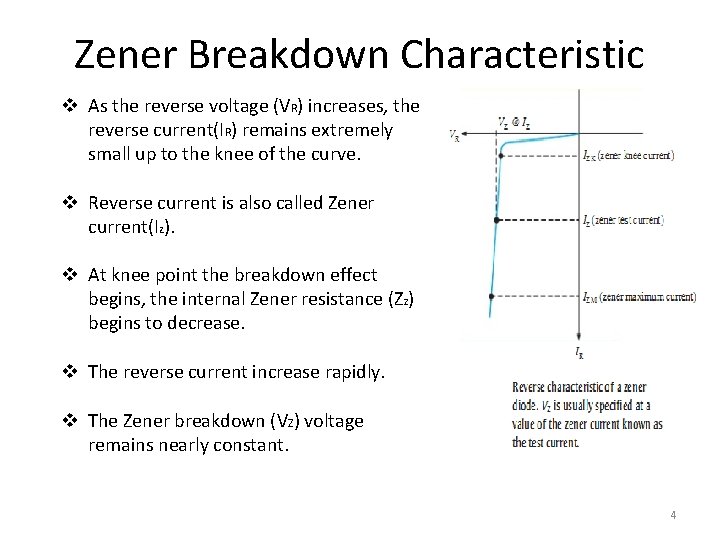
Zener Breakdown Characteristic v As the reverse voltage (VR) increases, the reverse current(IR) remains extremely small up to the knee of the curve. v Reverse current is also called Zener current(Iz). v At knee point the breakdown effect begins, the internal Zener resistance (ZZ) begins to decrease. v The reverse current increase rapidly. v The Zener breakdown (VZ) voltage remains nearly constant. 4
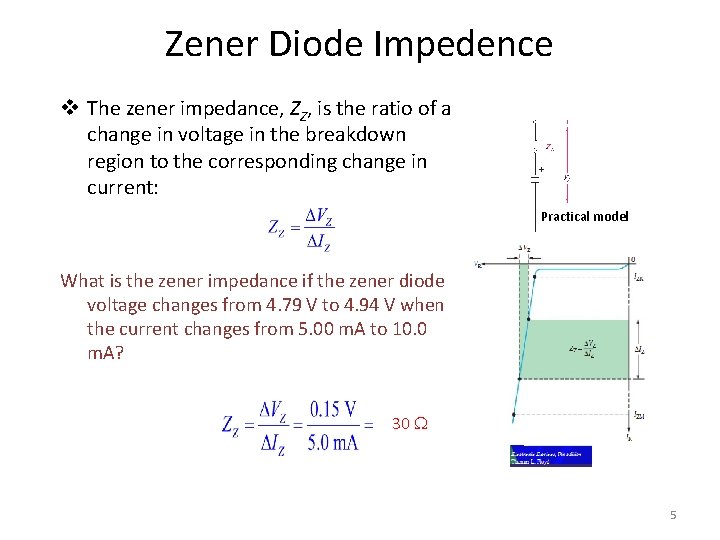
Zener Diode Impedence v The zener impedance, ZZ, is the ratio of a change in voltage in the breakdown region to the corresponding change in current: Practical model What is the zener impedance if the zener diode voltage changes from 4. 79 V to 4. 94 V when the current changes from 5. 00 m. A to 10. 0 m. A? 30 W 5
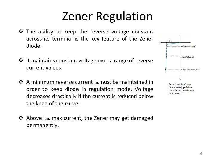
Zener Regulation v The ability to keep the reverse voltage constant across its terminal is the key feature of the Zener diode. v It maintains constant voltage over a range of reverse current values. v A minimum reverse current IZK must be maintained in order to keep diode in regulation mode. Voltage decreases drastically if the current is reduced below the knee of the curve. v Above IZM, max current, the Zener may get damaged permanently. 6
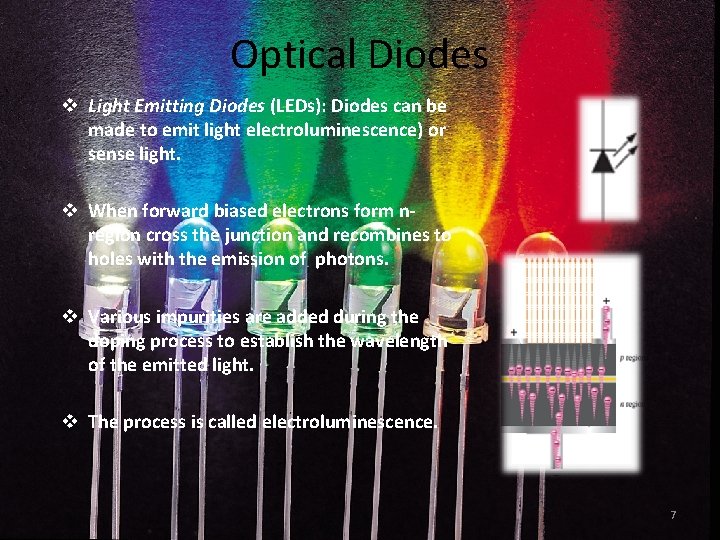
Optical Diodes v Light Emitting Diodes (LEDs): Diodes can be made to emit light electroluminescence) or sense light. v When forward biased electrons form nregion cross the junction and recombines to holes with the emission of photons. v Various impurities are added during the doping process to establish the wavelength of the emitted light. v The process is called electroluminescence. 7

Light Emitting Diodes v LEDs vary widely in size and brightness – from small indicating lights and displays to highintensity LEDs that are used in traffic signals, outdoor signs, and general illumination. v LEDs are very efficient light emitters, and extremely reliable, so domain of uses getting wider. 8
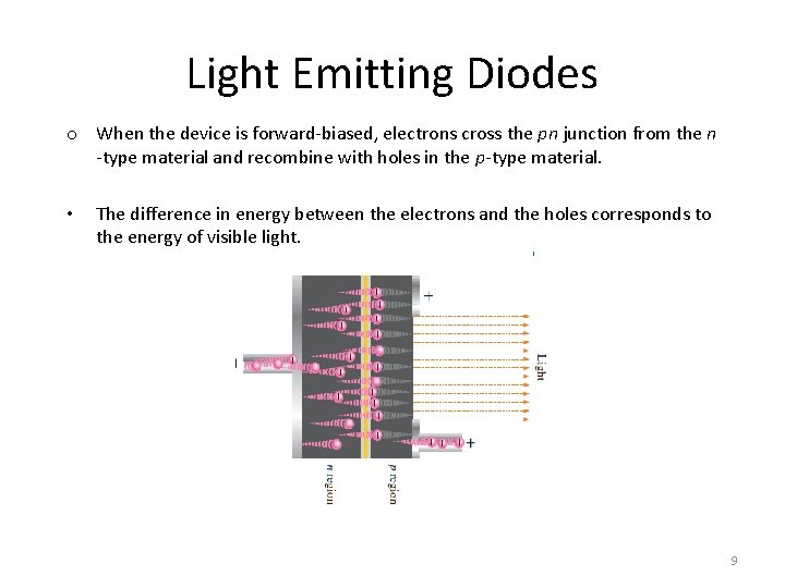
Light Emitting Diodes o When the device is forward-biased, electrons cross the pn junction from the n -type material and recombine with holes in the p-type material. • The difference in energy between the electrons and the holes corresponds to the energy of visible light. 9
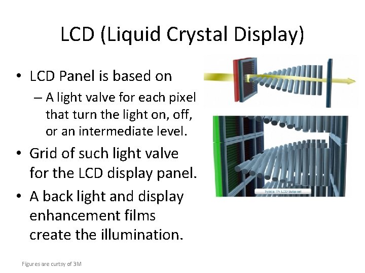
LCD (Liquid Crystal Display) • LCD Panel is based on – A light valve for each pixel that turn the light on, off, or an intermediate level. • Grid of such light valve for the LCD display panel. • A back light and display enhancement films create the illumination. Figures are curtsy of 3 M
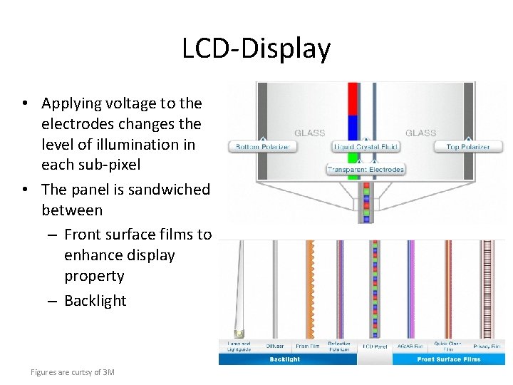
LCD-Display • Applying voltage to the electrodes changes the level of illumination in each sub-pixel • The panel is sandwiched between – Front surface films to enhance display property – Backlight Figures are curtsy of 3 M
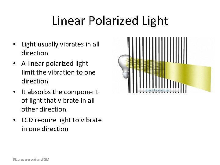
Linear Polarized Light • Light usually vibrates in all direction • A linear polarized light limit the vibration to one direction • It absorbs the component of light that vibrate in all other direction. • LCD require light to vibrate in one direction Figures are curtsy of 3 M
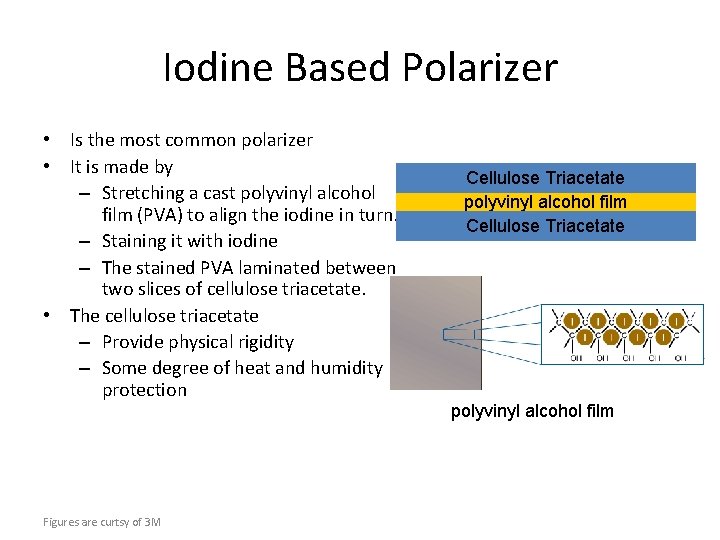
Iodine Based Polarizer • Is the most common polarizer • It is made by – Stretching a cast polyvinyl alcohol film (PVA) to align the iodine in turn. – Staining it with iodine – The stained PVA laminated between two slices of cellulose triacetate. • The cellulose triacetate – Provide physical rigidity – Some degree of heat and humidity protection Figures are curtsy of 3 M Cellulose Triacetate polyvinyl alcohol film
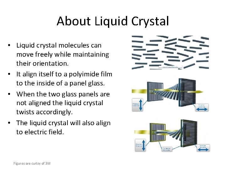
About Liquid Crystal • Liquid crystal molecules can move freely while maintaining their orientation. • It align itself to a polyimide film to the inside of a panel glass. • When the two glass panels are not aligned the liquid crystal twists accordingly. • The liquid crystal will also align to electric field. Figures are curtsy of 3 M
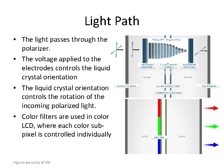
Light Path • The light passes through the polarizer. • The voltage applied to the electrodes controls the liquid crystal orientation • The liquid crystal orientation controls the rotation of the incoming polarized light. • Color filters are used in color LCD, where each color subpixel is controlled individually Figures are curtsy of 3 M
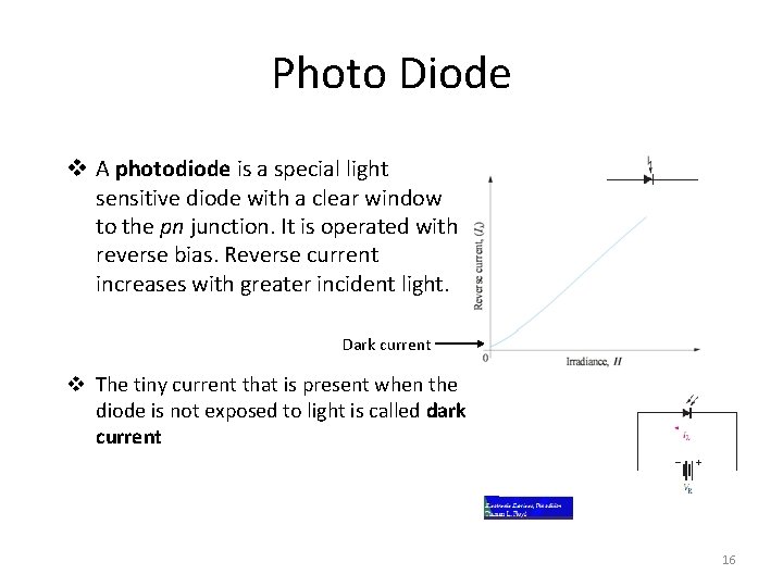
Photo Diode v A photodiode is a special light sensitive diode with a clear window to the pn junction. It is operated with reverse bias. Reverse current increases with greater incident light. Dark current v The tiny current that is present when the diode is not exposed to light is called dark current 16
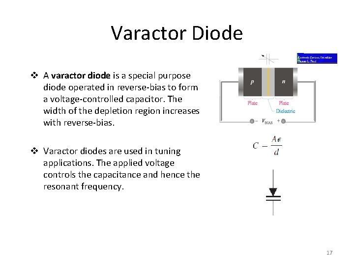
Varactor Diode v A varactor diode is a special purpose diode operated in reverse-bias to form a voltage-controlled capacitor. The width of the depletion region increases with reverse-bias. v Varactor diodes are used in tuning applications. The applied voltage controls the capacitance and hence the resonant frequency. 17
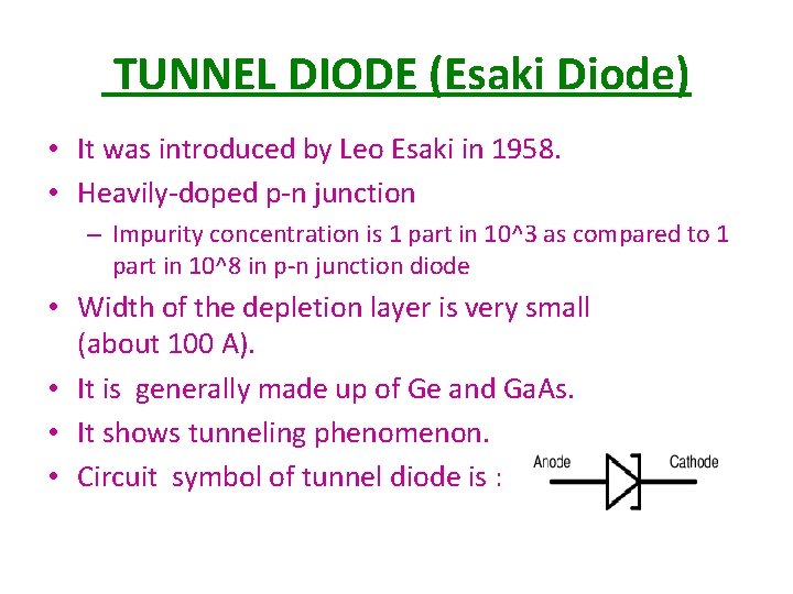
TUNNEL DIODE (Esaki Diode) • It was introduced by Leo Esaki in 1958. • Heavily-doped p-n junction EV – Impurity concentration is 1 part in 10^3 as compared to 1 part in 10^8 in p-n junction diode • Width of the depletion layer is very small (about 100 A). • It is generally made up of Ge and Ga. As. • It shows tunneling phenomenon. • Circuit symbol of tunnel diode is :
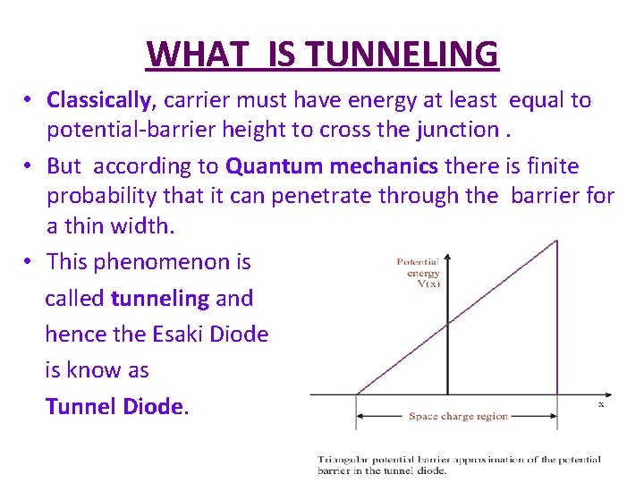
WHAT IS TUNNELING • Classically, carrier must have energy at least equal to potential-barrier height to cross the junction. • But according to Quantum mechanics there is finite probability that it can penetrate through the barrier for a thin width. • This phenomenon is called tunneling and hence the Esaki Diode is know as Tunnel Diode.
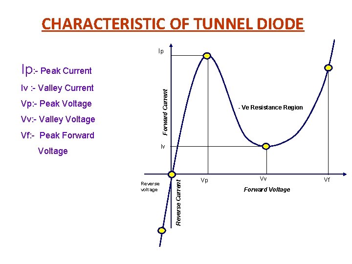
CHARACTERISTIC OF TUNNEL DIODE Ip Ip: - Peak Current Forward Current Iv : - Valley Current Vp: - Peak Voltage Vv: - Valley Voltage Vf: - Peak Forward - Ve Resistance Region Reverse voltage Reverse Current Iv Voltage Vp Vv Forward Voltage Vf
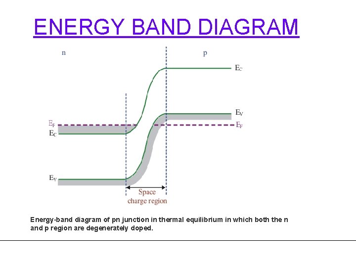
ENERGY BAND DIAGRAM Energy-band diagram of pn junction in thermal equilibrium in which both the n and p region are degenerately doped.
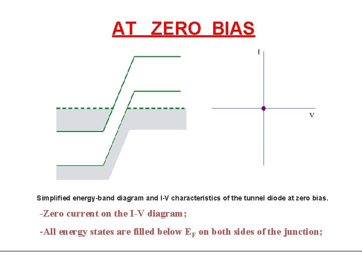
AT ZERO BIAS Simplified energy-band diagram and I-V characteristics of the tunnel diode at zero bias. -Zero current on the I-V diagram; -All energy states are filled below EF on both sides of the junction;
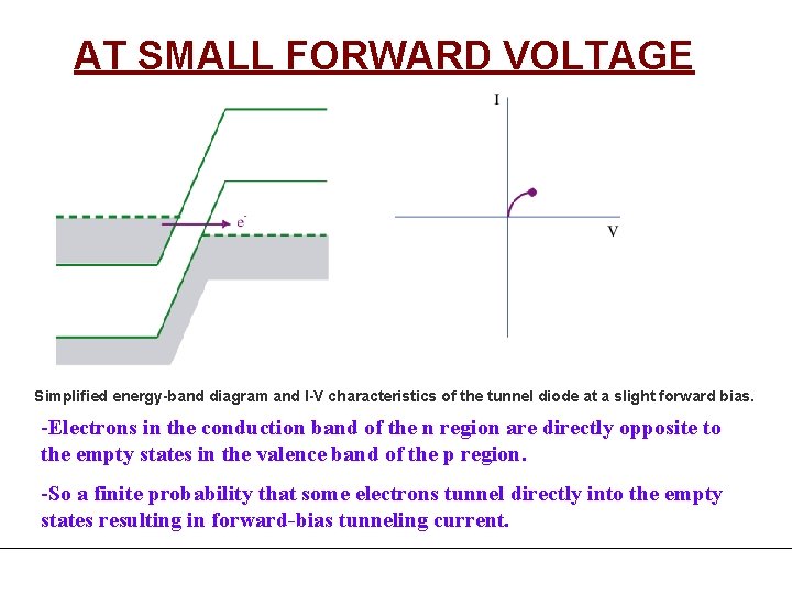
AT SMALL FORWARD VOLTAGE Simplified energy-band diagram and I-V characteristics of the tunnel diode at a slight forward bias. -Electrons in the conduction band of the n region are directly opposite to the empty states in the valence band of the p region. -So a finite probability that some electrons tunnel directly into the empty states resulting in forward-bias tunneling current.
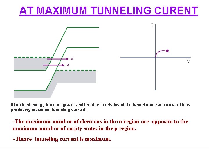
AT MAXIMUM TUNNELING CURENT Simplified energy-band diagraam and I-V characteristics of the tunnel diode at a forward bias producing maximum tunneling current. -The maximum number of electrons in the n region are opposite to the maximum number of empty states in the p region. - Hence tunneling current is maximum.
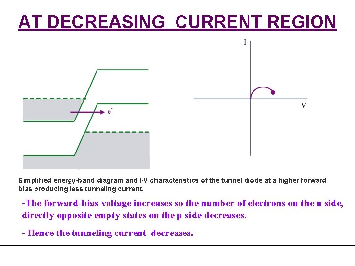
AT DECREASING CURRENT REGION Simplified energy-band diagram and I-V characteristics of the tunnel diode at a higher forward bias producing less tunneling current. -The forward-bias voltage increases so the number of electrons on the n side, directly opposite empty states on the p side decreases. - Hence the tunneling current decreases.
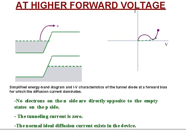
AT HIGHER FORWARD VOLTAGE Simplified energy-band diagram and I-V characteristics of the tunnel diode at a forward bias for which the diffusion current dominates. -No electrons on the n side are directly opposite to the empty states on the p side. - The tunneling current is zero. -The normal ideal diffusion current exists in the device.
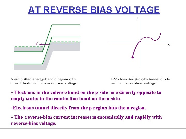
AT REVERSE BIAS VOLTAGE - Electrons in the valence band on the p side are directly opposite to empty states in the conduction band on the n side. -Electrons tunnel directly from the p region into the n region. - The reverse-bias current increases monotonically and rapidly with reverse-bias voltage.
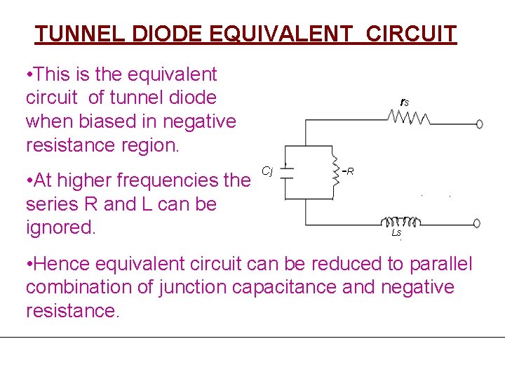
TUNNEL DIODE EQUIVALENT CIRCUIT • This is the equivalent circuit of tunnel diode when biased in negative resistance region. • At higher frequencies the series R and L can be ignored. rs Cj -R Ls • Hence equivalent circuit can be reduced to parallel combination of junction capacitance and negative resistance.
SCR: The SCR is the most important special semiconductor device. This device is popular for its Forward-Conducting and Reverse-blocking characteristics. SCR can be used in high-power devices. For example, in the central processing unit of the computer, the SCR is used in switch mode power supply (SMPS). The DIAC, a combination of two Shockley Diodes, and the TRIAC, a combination of two SCRs connected anti-parallelly are important power-control devices. The UJT is also used as an efficient switching device.
SILICON-CONTROLLED RECTIFIER (SCR) The silicon-controlled rectifier or semiconductor controlled rectifier is a two-state device used for efficient power control. SCR is the parent member of the thyristor family and is used in high-power electronics. Its constructional features, physical operation and characteristics are explained in the following sections.

Constructional Features The SCR is a four-layer structure, either p–n–p–n or n–p–n– p, that effectively blocks current through two terminals until it is turned ON by a small-signal at a third terminal. The SCR has two states: a high-current low-impedance ON state and a low-current high-impedance OFF state. The basic transistor action in a four-layer p–n–p–n structure is analysed first with only two terminals, and then the third control input is introduced.
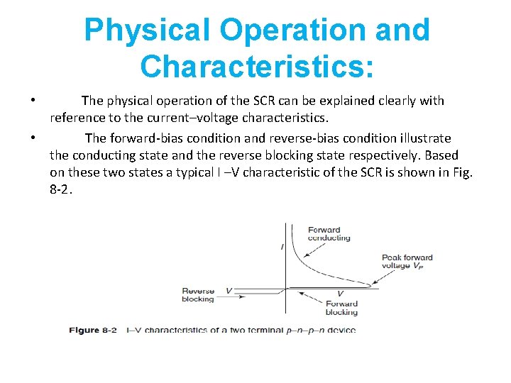
Physical Operation and Characteristics: • The physical operation of the SCR can be explained clearly with reference to the current–voltage characteristics. • The forward-bias condition and reverse-bias condition illustrate the conducting state and the reverse blocking state respectively. Based on these two states a typical I –V characteristic of the SCR is shown in Fig. 8 -2.
SCR in Forward Bias: • There are two different states in which we can examine the SCR in the forward-biased condition: (i) The high- impedance or forward-blocking state (ii) The low-impedance or forward-conducting state At a critical peak forward voltage Vp, the SCR switches from the blocking state to the conducting state, as shown in Fig. 8 -2. • A positive voltage places junction j 1 and j 3 under forward-bias, and the centre junction j 2 under reverse-bias. • The for ward voltage in the blocking state appears across the reversebiased junc tion j 2 as the applied voltage V is increased. The voltage from the anode A to cathode C, as shown in Fig. 8 -1, is very small after switching to the forward-conducting state, and all three junctions are forward-biased. The junction j 2 switches from reverse-bias to forward-bias. .
SCR in Reverse Bias: v In the reverse-blocking state the junctions j 1 and j 3 are reverse-biased, and j 2 is forward-biased. v The supply of electrons and holes to junction j 2 is restricted, and due to thermal generation of electron–hole pairs near junctions j 1 and j 2 the device current is a small saturation current. v In the reverse blocking condition the current remains small until avalanche breakdown occurs at a large reverse-bias of several thousand volts. v An SCR p–n–p–n structure is equivalent to one p–n–p transistor and one n– p–n transistor sharing some common terminals. v Collector current I C 1 = α 1 i + I CO 1 having a transfer ratio α 1 for the p–n–p. v Collector current I C 2 =α 2 i + I CO 2 having a transfer ratio a 2 for the n–p–n. v ICO 1 and ICO 2 stand for the respective collector-saturation currents. I C 1 = α 1 i + I CO 1 = I B 2 ………………. (8 -1) I C 2 = α 2 i + I CO 2 = I B 1 ……………… (8 -2)
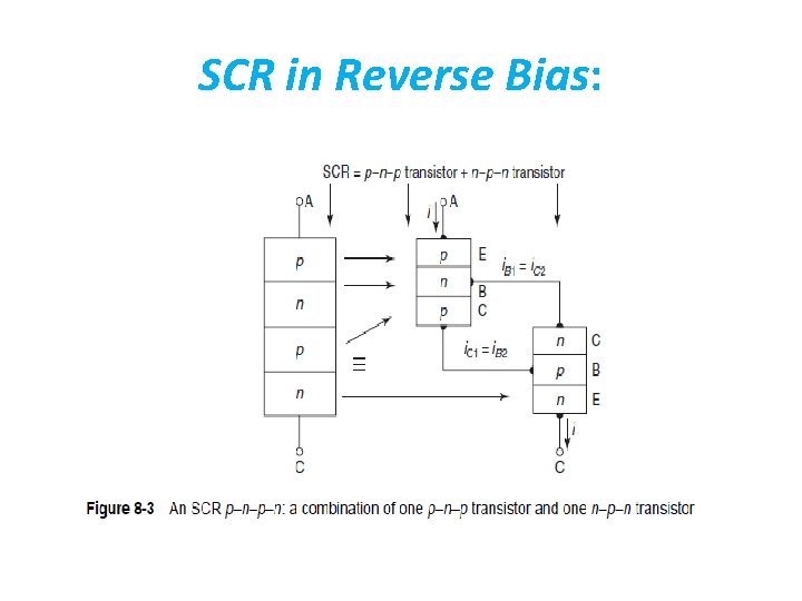
SCR in Reverse Bias:
SCR in Reverse Bias: • • • The total current through the SCR is the sum of i. C 1 and i. C 2: I C 1 + I = i ………………. . (8 -3) Substituting the values of collector current from Eqs. (8 -1) and (8 -2) in Eq. (8 -3) we get: i (α 1 + α 2) + I CO 1 + I CO 2 = i i = (I CO 1 + I CO 2 ) /(1 - α 1 + α 2) ………………. . (8 -4) Case I: When (α 1 + α 2) → 1, then the SCR current i → infinite. As the sum of the values of alphas tends to unity, the SCR current i increases rapidly. The derivation is no longer valid as (α 1 + α 2) equals unity. Case II: When (α 1 + α 2 → 0, i. e. , when the summation value of alphas goes to zero, the SCR resultant current can be expressed as: i = I CO 1 + I CO 2 ………………. (8 -5) The current, i, passing through the SCR is very small. It is the combined collectorsaturation currents of the two equivalent transistors as long as the sum (α 1 + α 2) is very small or almost near zero.
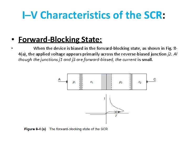
I–V Characteristics of the SCR: • Forward-Blocking State: • When the device is biased in the forward-blocking state, as shown in Fig. 84(a), the applied voltage appears primarily across the reverse-biased junction j 2. Al though the junctions j 1 and j 3 are forward-biased, the current is small.
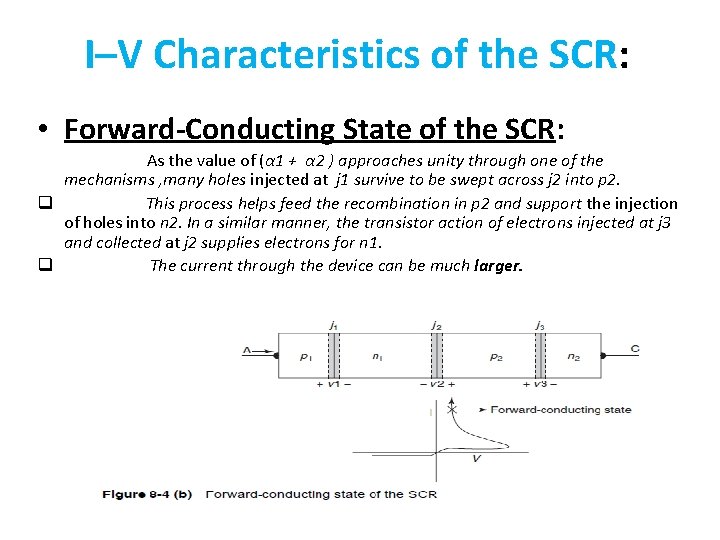
I–V Characteristics of the SCR: • Forward-Conducting State of the SCR: As the value of (α 1 + α 2 ) approaches unity through one of the mechanisms , many holes injected at j 1 survive to be swept across j 2 into p 2. q This process helps feed the recombination in p 2 and support the injection of holes into n 2. In a similar manner, the transistor action of electrons injected at j 3 and collected at j 2 supplies electrons for n 1. q The current through the device can be much larger.
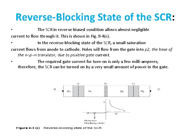
Reverse-Blocking State of the SCR: • The SCR in reverse-biased condition allows almost negligible current to flow through it. This is shown in Fig. 8 -4(c). • In the reverse-blocking state of the SCR, a small saturation current flows from anode to cathode. Holes will flow from the gate into p 2, the base of the n–p–n transistor, due to positive gate current. • The required gate current for turn-on is only a few milli-amperes, therefore, the SCR can be turned on by a very small amount of power in the gate.
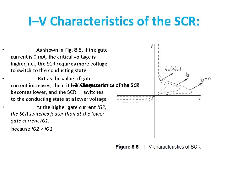
I–V Characteristics of the SCR: As shown in Fig. 8 -5, if the gate current is 0 m. A, the critical voltage is higher, i. e. , the SCR requires more voltage to switch to the conducting state. • But as the value of gate I–V Characteristics of the SCR: current increases, the critical voltage becomes lower, and the SCR switches to the conducting state at a lower voltage. • At the higher gate current IG 2, the SCR switches faster than at the lower gate current IG 1, because IG 2 > IG 1. •
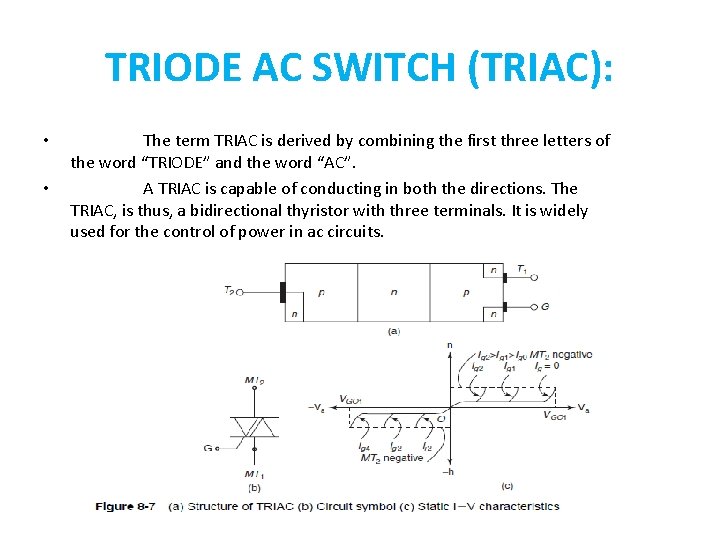
TRIODE AC SWITCH (TRIAC): • • The term TRIAC is derived by combining the first three letters of the word “TRIODE” and the word “AC”. A TRIAC is capable of conducting in both the directions. The TRIAC, is thus, a bidirectional thyristor with three terminals. It is widely used for the control of power in ac circuits.

Constructional Features: Depending upon the polarity of the gate pulse and the biasing conditions, the main four-layer structure that turns ON by a regenerative process could be one of p 1 n 1, p 2 n 2, p 1 n 1 p 2 n 3, or p 2 n 1 p 1 n 4, as shown in Fig. 8 -8.

Advantages of the TRIAC: • The TRIAC has the following advantages: (i) They can be triggered with positive- or negative-polarity voltage. (ii) They need a single heat sink of slightly larger size. (iii) They need a single fuse for protection, which simplifies their construction. (iv) In some dc applications, the SCR has to be connected with a parallel diode for protection against reverse voltage, whereas a TRIAC may work without a diode, as safe breakdown in either direction is possible.
Disadvantages of the TRIAC: • The TRIAC has the following disadvantages: (i) TRIACs have low dv/dt ratings compared to SCRs. (ii) Since TRIACs can be triggered in either direction, the trigger circuits with TRIACs needs careful consideration. (iii) Reliability of TRIACs is less than that of SCRs.

Simple Applications of the TRIAC: • The TRIAC as a bidirectional thyristor has various applications. Some of the popular applications of the TRIAC are as follows: (i) In speed control of single-phase ac series or universal motors. (ii) In food mixers and portable drills. (iii) In lamp dimming and heating control. (iv) In zero-voltage switched ac relay.
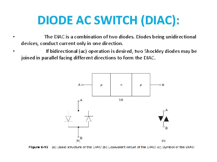
DIODE AC SWITCH (DIAC): • • The DIAC is a combination of two diodes. Diodes being unidirectional devices, conduct current only in one direction. If bidirectional (ac) operation is desired, two Shockley diodes may be joined in parallel facing different directions to form the DIAC.

Constructional Features: • The construction of DIAC looks like a transistor but there are major differences. • They are as follows: (i) All the three layers, p–n–p or n–p–n, are equally doped in the DIAC, whereas in the BJT there is a gradation of doping. The emitter is highly doped, the collector is lightly doped, and the base is moderately doped. • (ii) The DIAC is a two-terminal diode as opposed to the BJT, which is a threeterminal device.
Physical Operation and Characteristics: • The main characteristics are of the DIAC are as follows: (i) Break over voltage (ii) Voltage symmetry (iii) Break-back voltage (iv) Break over current (v) Lower power dissipation • Although most DIACs have symmetric switching voltages, asymmetric DIACs are also available. Typical DIACs have a power dissipations ranging from 1/2 to 1 watt.
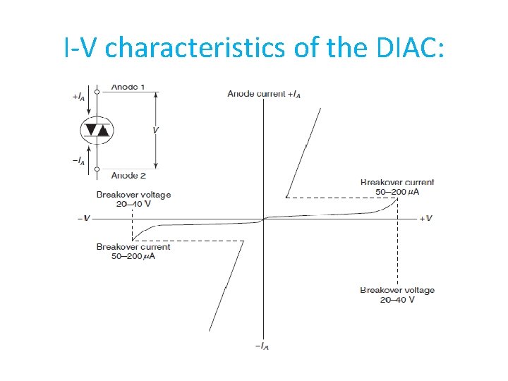
I-V characteristics of the DIAC:
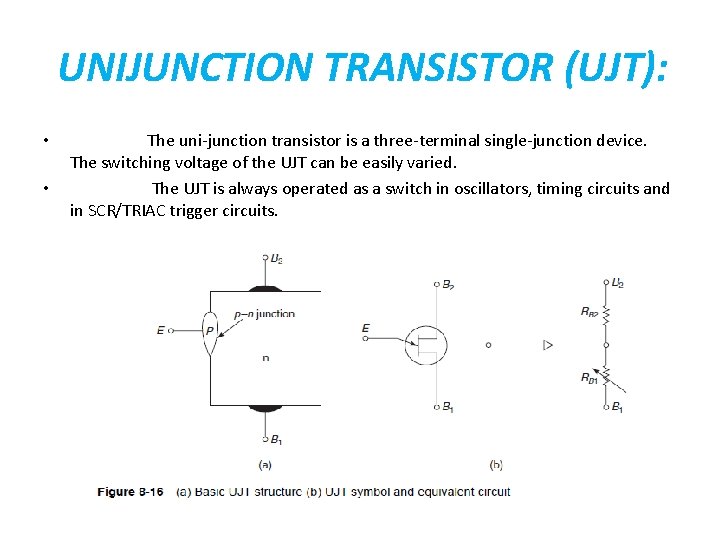
UNIJUNCTION TRANSISTOR (UJT): • • The uni-junction transistor is a three-terminal single-junction device. The switching voltage of the UJT can be easily varied. The UJT is always operated as a switch in oscillators, timing circuits and in SCR/TRIAC trigger circuits.
Constructional Features: • The UJT structure consists of a lightly doped n-type silicon bar provided with ohmic contacts on either side. • The two end connections are called base B 1 and base B 2. A small heavily doped p-region is alloyed into one side of the bar. This p-region is the UJT emitter (E) that forms a p–n junction with the bar. Between base B 1 and base B 2, the resistance of the n-type bar called inter-base resistance (RB ) and is in the order of a few kilo ohm. • • • This inter-base resistance can be broken up into two resistances—the resistance from B 1 to the emitter is RB 1 and the resistance from B 2 to the emitter is RB 2. Since the emitter is closer to B 2 the value of RB 1 is greater than RB 2. • Total resistance is given by: RB = RB 1 + RB 2
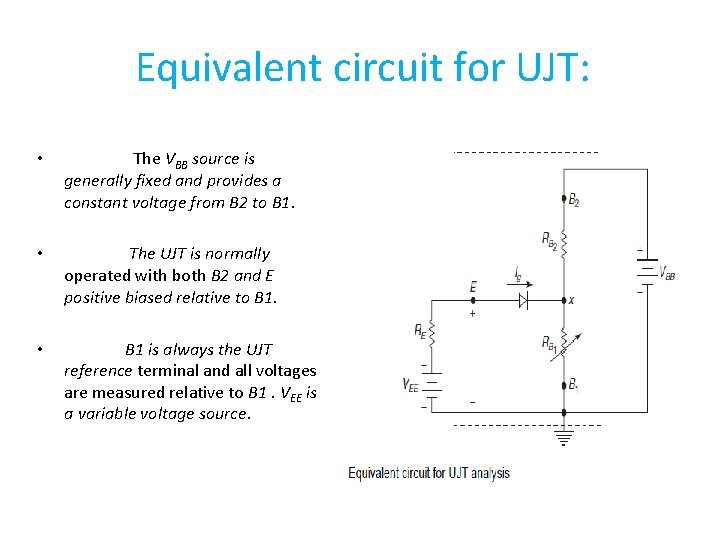
Equivalent circuit for UJT: • The VBB source is generally fixed and provides a constant voltage from B 2 to B 1. • The UJT is normally operated with both B 2 and E positive biased relative to B 1. • B 1 is always the UJT reference terminal and all voltages are measured relative to B 1. VEE is a variable voltage source.
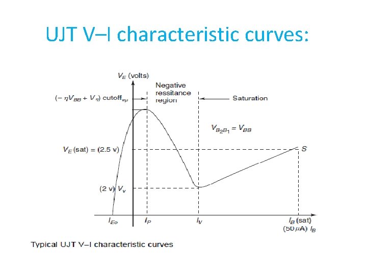
UJT V–I characteristic curves:
ON State of the UJT Circuit: • • As VEE increases, the UJT stays in the OFF state until VE approaches the peak point value V P. As VE approaches VP the p–n junction becomes forwardbiased and begins to conduct in the opposite direction. As a result IE becomes positive near the peak point P on the VE - IE curve. When VE exactly equals VP the emitter current equals IP. • At this point holes from the heavily doped emitter are injected into the n-type bar, especially into the B 1 region. The bar, which is lightly doped, offers very little chance for these holes to recombine. • The lower half of the bar becomes replete with additional current carriers (holes) and its resistance RB is drastically reduced; the decrease in BB 1 causes Vx to drop. This drop, in turn, causes the diode to become more forward-biased and IE increases even further. •
OFF State of the UJT Circuit: • • When a voltage VBB is applied across the two base terminals B 1 and B 2, the potential of point p with respect to B 1 is given by: VP =[VBB/ (RB 1 +RB 2)]*RB 1=η*RB 1 η is called the intrinsic stand off ratio with its typical value lying between 0. 5 and 0. 8. • The VEE source is applied to the emitter which is the p-side. Thus, the emitter diode will be reverse-biased as long as VEE is less than Vx. This is OFF state and is shown on the VE - IE curve as being a very low current region. • In the OFF the UJT has a very high resistance between E and B 1, and IE is usually a negligible reverse leakage current. With no IE, the drop across RE is zero and the emitter voltage equals the source voltage.
Applications: • The UJT is very popular today mainly due to its high switching speed. • A few select applications of the UJT are as follows: (i) It is used to trigger SCRs and TRIACs (ii) It is used in non-sinusoidal oscillators (iii) It is used in phase control and timing circuits (iv) It is used in saw tooth generators (v) It is used in oscillator circuit design
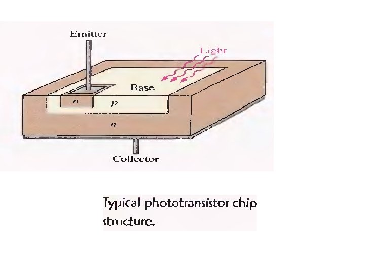
PHOTO TRANSSTOR • The phototransistor is a transistor in which base current is produced when light strikes the photosensitive semiconductor base region. • The collector-base P-N junction is exposed to incident light through a lens opening in the transistor package. • When there is no incident light, there is only a small thermally generated collector-to-emitter leakage current i. e. I(CEO), this is called the dark current and is typically in the n. A range.
When light strikes the collector-base pn junction, a base current is produced that is directly proportional to the light intensity. Since the actual photo generation of base current occurs in the collector-base region, the larger the physical area of this region, the more base current is generated. A phototransistor does not activated at every type of wave lengths of light.
q The phototransistor is similar to a regular BJT except that the base current is produced and controlled by light instead of a voltage source. q The phototransistor effectively converts variations in light energy to an electrical signal q The collector-base pn junction is exposed to incident light through a lens opening in the transistor package. q The phototransistor is a transistor in which base current is produced when light strikes the photosensitive semiconductor base region. q When there is no incident light, there is only a small thermally generated collector-toemitter leakage current i. e. I(CEO), this is called the dark current and is typically in the range of n. A.
q When light strikes the collector-base pn junction, a base current, Iλ, is produced that is directly proportional to the light intensity. q This action produces a collector current that increases with Iλ. q Except for the way base current is generated, the phototransistor behaves as a conventional BJT. q In many cases there is no electrical connection to the base q The relationship between the collector current and the light-generated base current in a phototransistor is IC = βDC * Iλ. 60
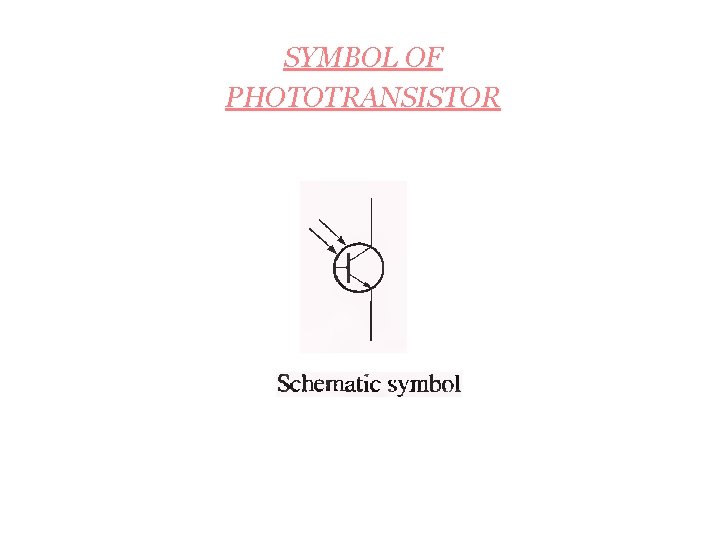
SYMBOL OF PHOTOTRANSISTOR
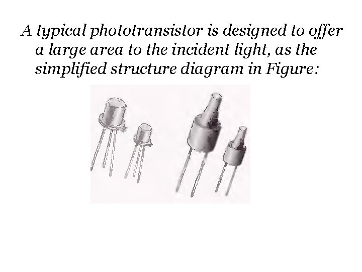
A typical phototransistor is designed to offer a large area to the incident light, as the simplified structure diagram in Figure:
Phototransistor are of two types. 1. Three Lead Phototransistor. 2. Two Lead Phototransistor.
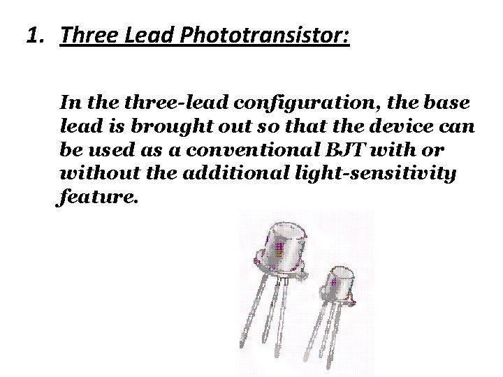
1. Three Lead Phototransistor: In the three-lead configuration, the base lead is brought out so that the device can be used as a conventional BJT with or without the additional light-sensitivity feature.
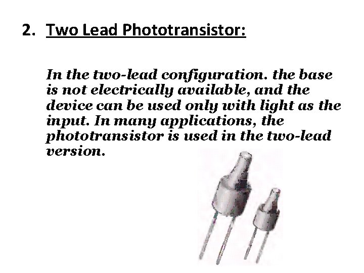
2. Two Lead Phototransistor: In the two-lead configuration. the base is not electrically available, and the device can be used only with light as the input. In many applications, the phototransistor is used in the two-lead version.
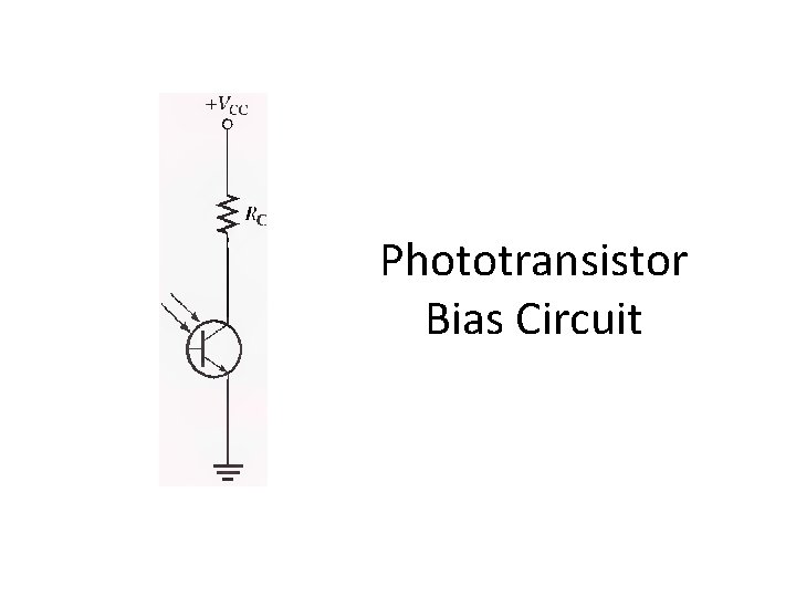
Phototransistor Bias Circuit
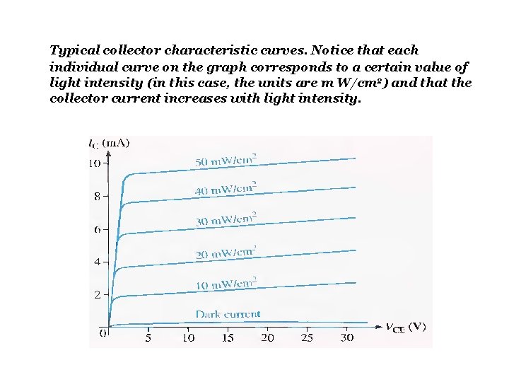
Typical collector characteristic curves. Notice that each individual curve on the graph corresponds to a certain value of light intensity (in this case, the units are m W/cm 2) and that the collector current increases with light intensity.
IR EMITTERS • An infrared emitter, or IR emitter, is a source of light energy in the infrared spectrum. It is a light emitting diode (LED) that is used in order to transmit infrared signals from a remote control. • In general, the more they are in quantity and the better the emitters are, the stronger and wider the resulting signal is. • A remote with strong emitters can often be used without directly pointing at the desired device. Infrared emitters are also partly responsible for limits on the range of frequencies that can be controlled. • An IR emitter generates infrared light that transmits information and commands from one device to another. • Typically one device receives the signal then passes the infrared (IR) signal through the emitter to another device.
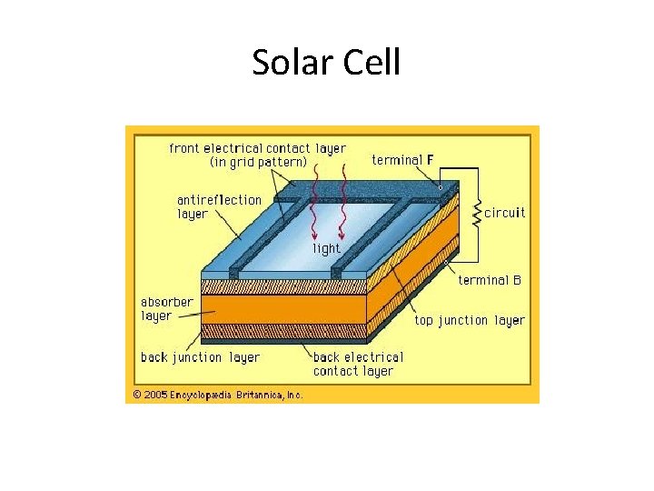
Solar Cell
• Solar cell, also called photovoltaic cell, any device that directly converts the energy in light into electrical energy through the photovoltaic effect. The overwhelming majority of solar cells are fabricated from silicon—with increasing efficiency and lowering cost as the materials range from amorphous(noncrystalline) to polycrystalline to crystalline (single crystal) silicon forms. Unlike batteries or fuel cells, solar cells do not utilize chemical reactions or require fuel to produce electric power, and, unlike electric generators, they do not have any moving parts.
Schottky Barrier diode:
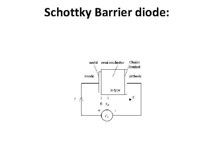
• A metal semiconductor junction is formed at one end, it is a unilateral junction. Another metal semiconductor contact is formed at the other end. It is an ideal Ohmic bilateral contact with no potential existing between metal and semiconductor and is non rectifying. The built-in potential across the open circuited Schottky barrier diode characterizes the Schottky barrier diode.
- Slides: 73