UNIT II Small Signal High Frequency Transistor Amplifier
- Slides: 24

UNIT II Small Signal High Frequency Transistor Amplifier Models

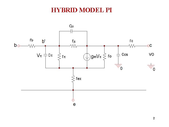
HYBRID MODEL PI 2

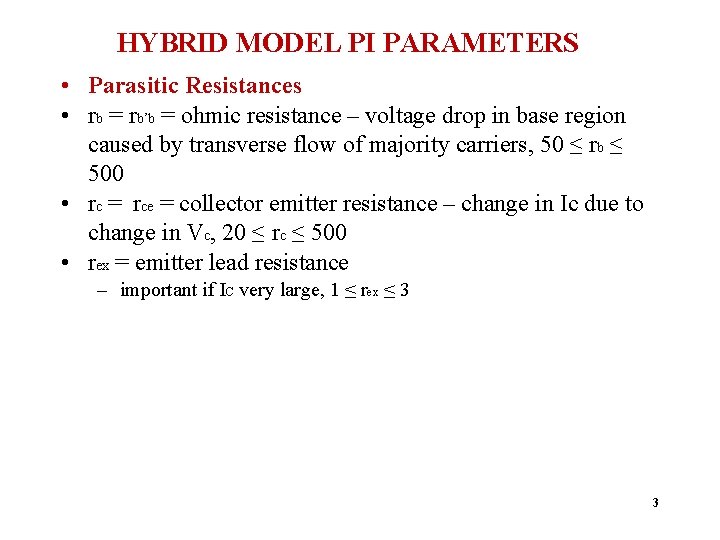
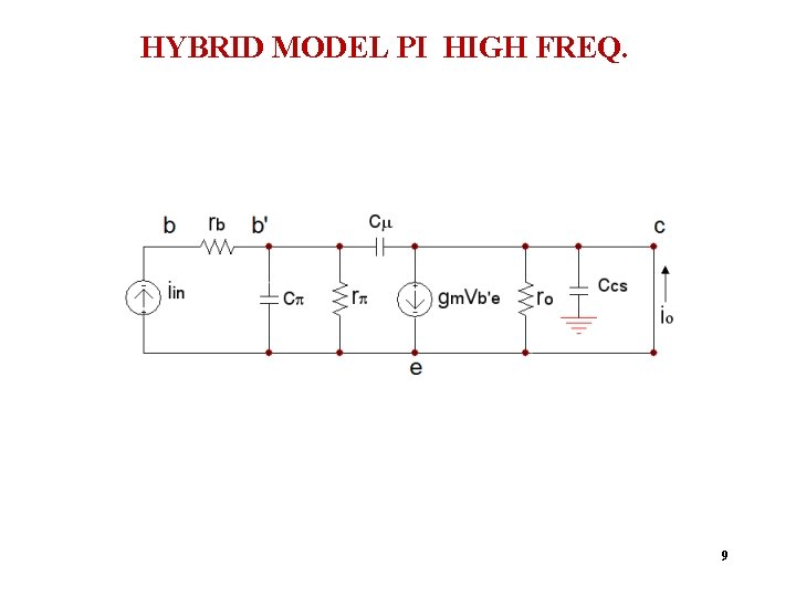
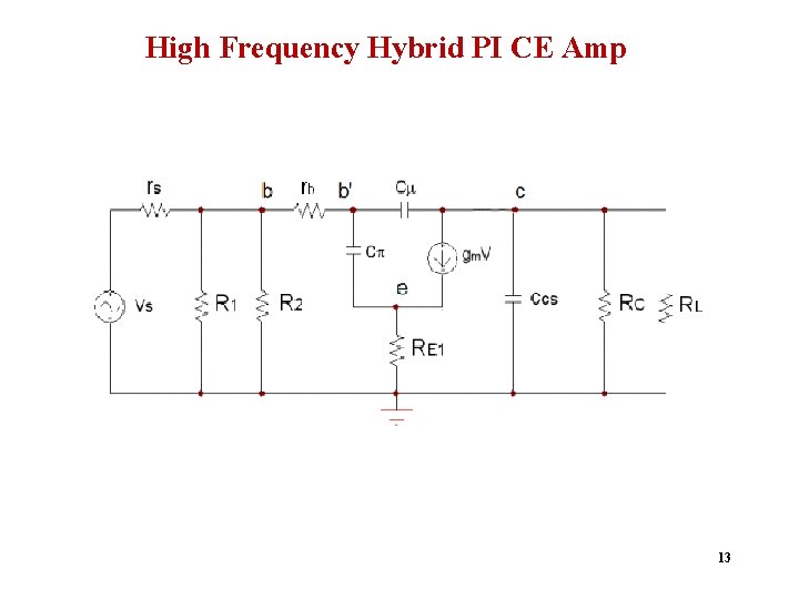
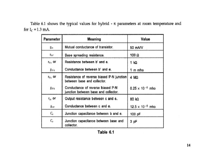
HYBRID MODEL PI PARAMETERS • Parasitic Resistances • rb = rb’b = ohmic resistance – voltage drop in base region caused by transverse flow of majority carriers, 50 ≤ rb ≤ 500 • rc = rce = collector emitter resistance – change in Ic due to change in Vc, 20 ≤ rc ≤ 500 • rex = emitter lead resistance – important if IC very large, 1 ≤ rex ≤ 3 3

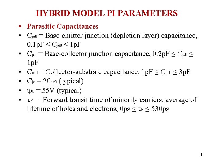
HYBRID MODEL PI PARAMETERS • Parasitic Capacitances • Cje 0 = Base-emitter junction (depletion layer) capacitance, 0. 1 p. F ≤ Cje 0 ≤ 1 p. F • C 0 = Base-collector junction capacitance, 0. 2 p. F ≤ C 0 ≤ 1 p. F • Ccs 0 = Collector-substrate capacitance, 1 p. F ≤ Ccs 0 ≤ 3 p. F • Cje = 2 Cje 0 (typical) • 0 =. 55 V (typical) • F = Forward transit time of minority carriers, average of lifetime of holes and electrons, 0 ps ≤ F ≤ 530 ps 4

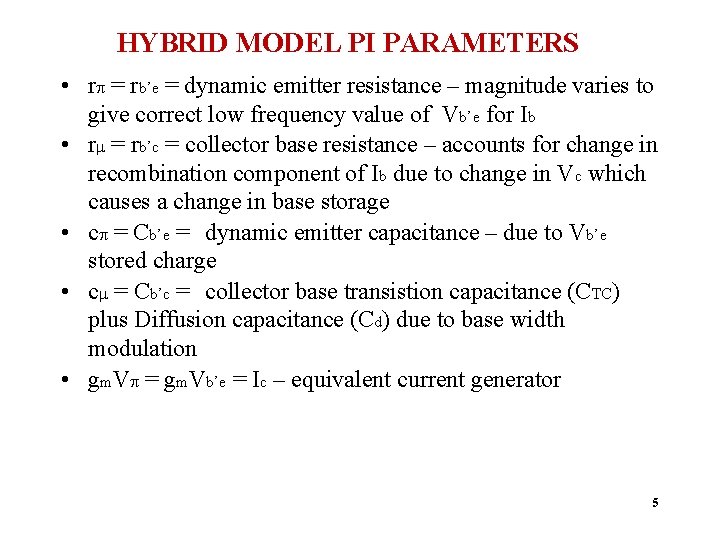
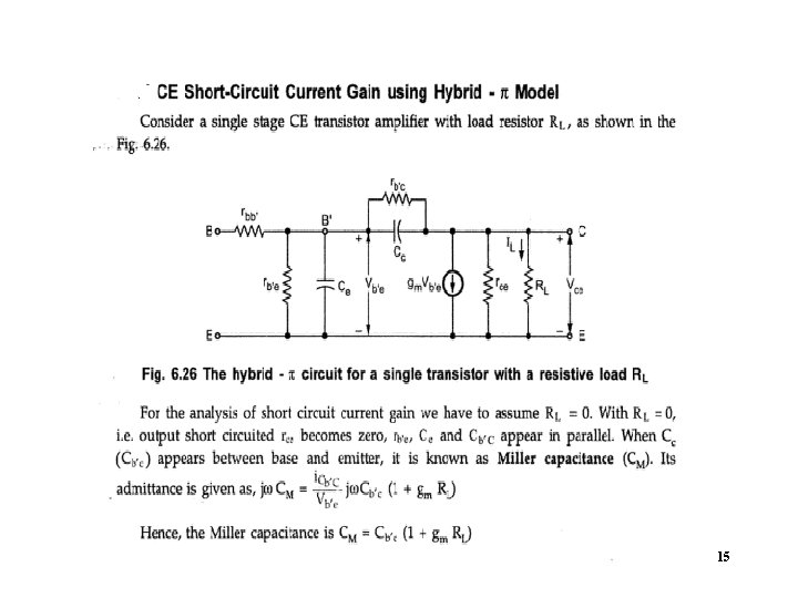
HYBRID MODEL PI PARAMETERS • r = rb’e = dynamic emitter resistance – magnitude varies to give correct low frequency value of Vb’e for Ib • r = rb’c = collector base resistance – accounts for change in recombination component of Ib due to change in Vc which causes a change in base storage • c = Cb’e = dynamic emitter capacitance – due to Vb’e stored charge • c = Cb’c = collector base transistion capacitance (CTC) plus Diffusion capacitance (Cd) due to base width modulation • gm. V = gm. Vb’e = Ic – equivalent current generator 5

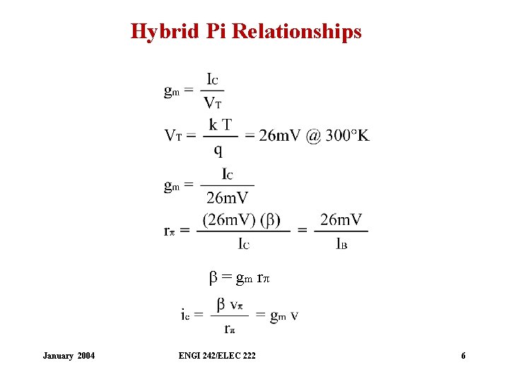
Hybrid Pi Relationships = g m r January 2004 ENGI 242/ELEC 222 6

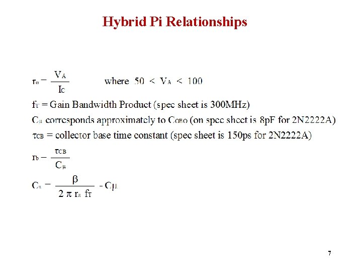
Hybrid Pi Relationships 7

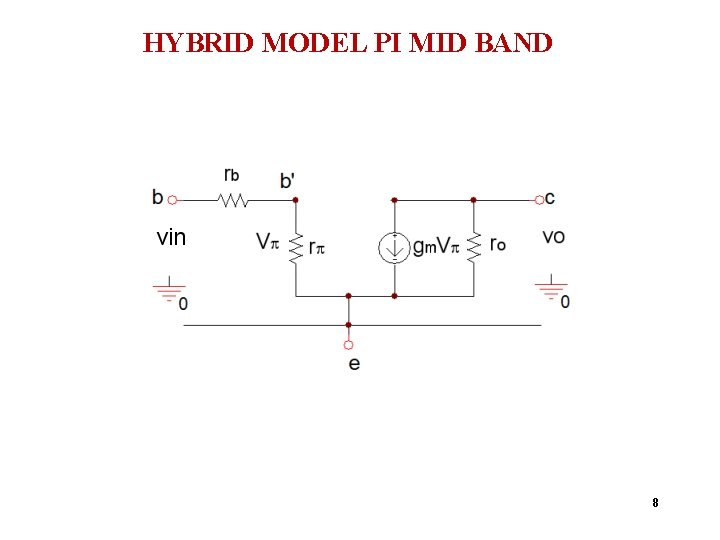
HYBRID MODEL PI MID BAND 8

HYBRID MODEL PI HIGH FREQ. 9

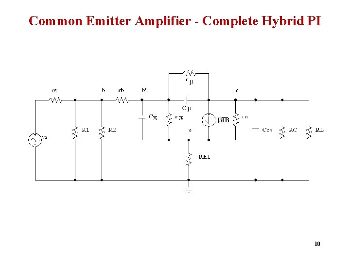
Common Emitter Amplifier - Complete Hybrid PI 10

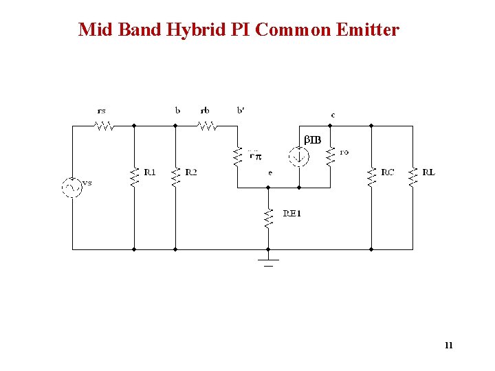
Mid Band Hybrid PI Common Emitter 11

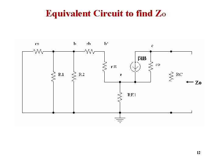
Equivalent Circuit to find ZO 12

High Frequency Hybrid PI CE Amp 13

14

15

16

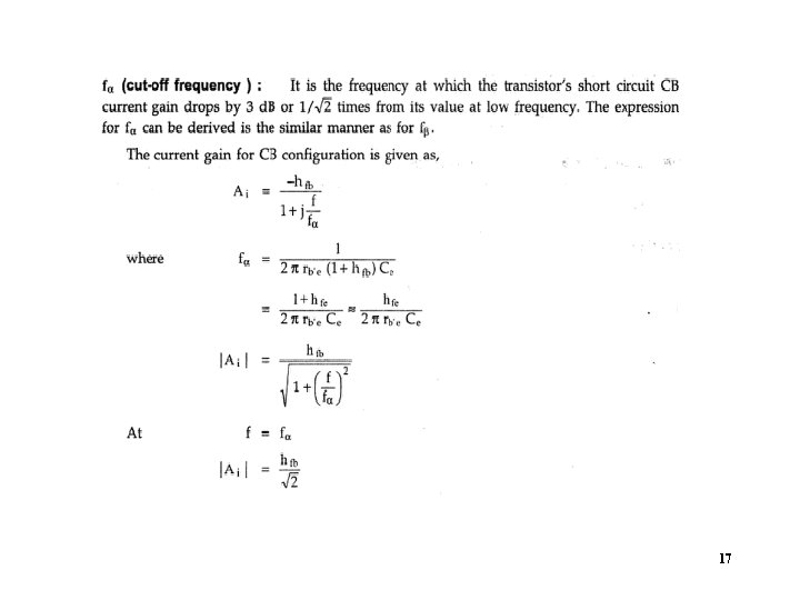
17

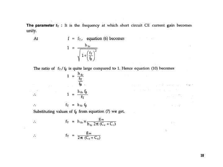
18

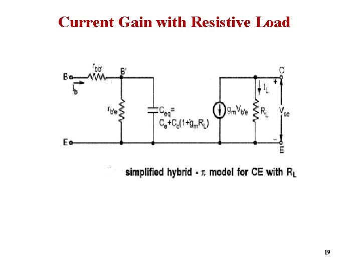
Current Gain with Resistive Load 19

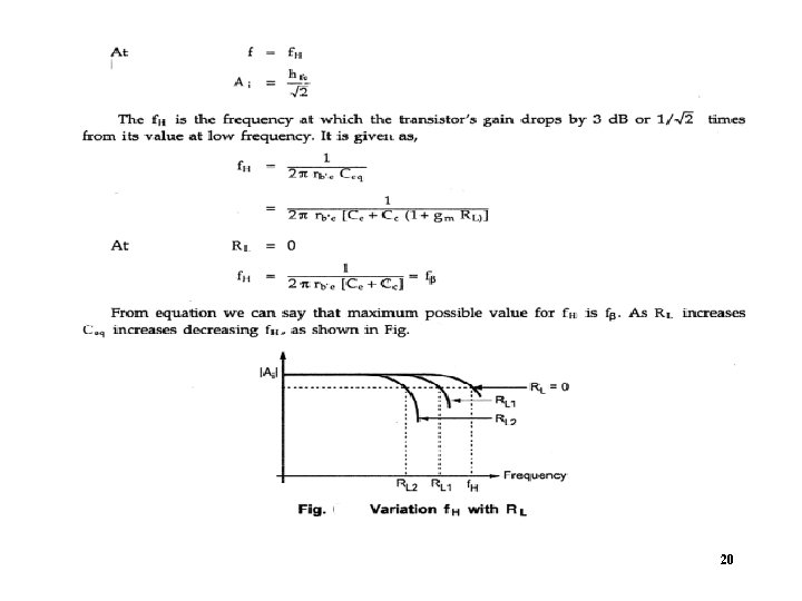
20

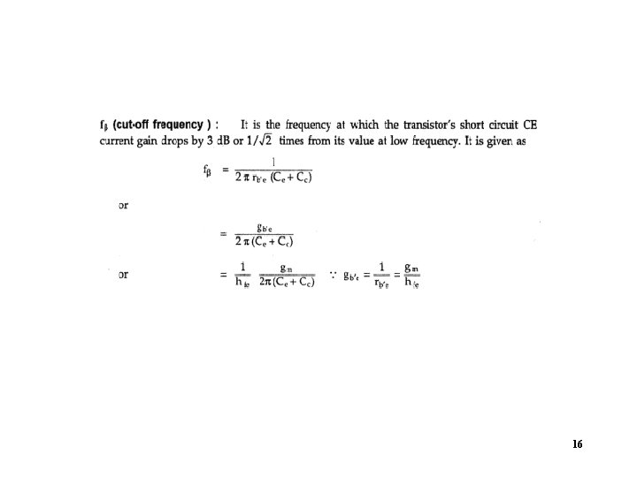
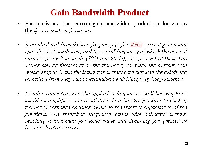
Gain Bandwidth Product • For transistors, the current-gain–bandwidth product is known as the f. T or transition frequency. • It is calculated from the low-frequency (a few KHz) current gain under specified test conditions, and the cutoff frequency at which the current gain drops by 3 decibels (70% amplitude); the product of these two values can be thought of as the frequency at which the current gain would drop to 1, and the transistor current gain between the cutoff and transition frequency can be estimated by dividing f. T by the frequency. • Usually, transistors must be applied at frequencies well below f. T to be useful as amplifiers and oscillators. In a bipolar junction transistor, frequency response declines owing to the internal capacitance of the junctions. The transition frequency varies with collector current, reaching a maximum for some value and declining for greater or lesser collector current. 21

22

23

24