Unit 8 Combinational Circuit Design and Simulation Using

Unit 8 Combinational Circuit Design and Simulation Using Gates Ku-Yaw Chang canseco@mail. dyu. edu. tw Assistant Professor, Department of Computer Science and Information Engineering Da-Yeh University 2004/03/11 Fundamentals of Logic Design
Contents 8. 1 Review of Combinational Circuit Design 8. 2 Design Circuits with Limited Gate Fan-In 8. 3 Gate Delays and Timing Diagrams 8. 4 Hazards in Combinational Logic 8. 5 Simulation and Testing of Logic Circuits 2004/03/11 Fundamentals of Logic Design 2
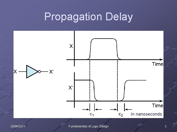
Propagation Delay In nanoseconds 2004/03/11 Fundamentals of Logic Design 3
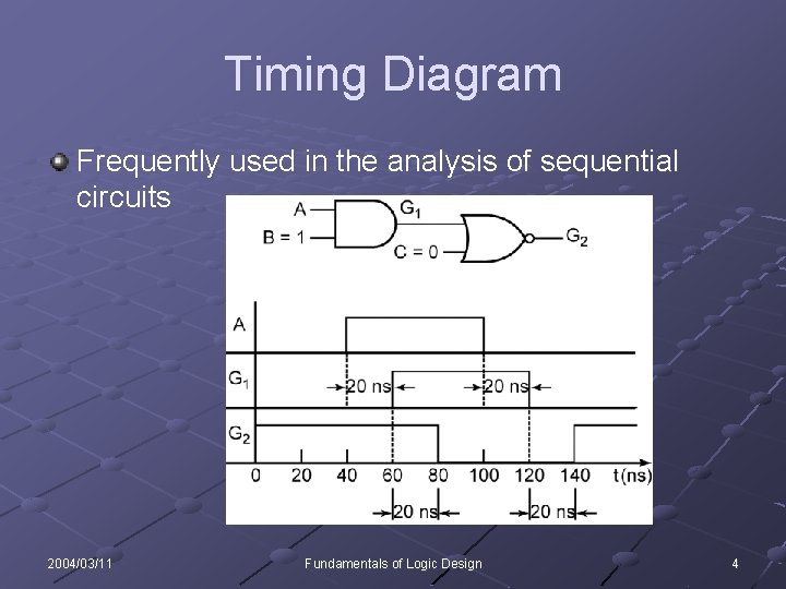
Timing Diagram Frequently used in the analysis of sequential circuits 2004/03/11 Fundamentals of Logic Design 4
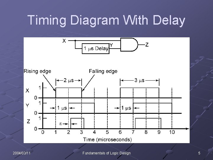
Timing Diagram With Delay 2004/03/11 Fundamentals of Logic Design 5
Contents 8. 1 Review of Combinational Circuit Design 8. 2 Design Circuits with Limited Gate Fan-In 8. 3 Gate Delays and Timing Diagrams 8. 4 Hazards in Combinational Logic 8. 5 Simulation and Testing of Logic Circuits 2004/03/11 Fundamentals of Logic Design 6
Hazards When the input to a combinational circuit changes, unwanted switching transients may appear in the output. n n Different paths Different propagation delays 2004/03/11 Fundamentals of Logic Design 7
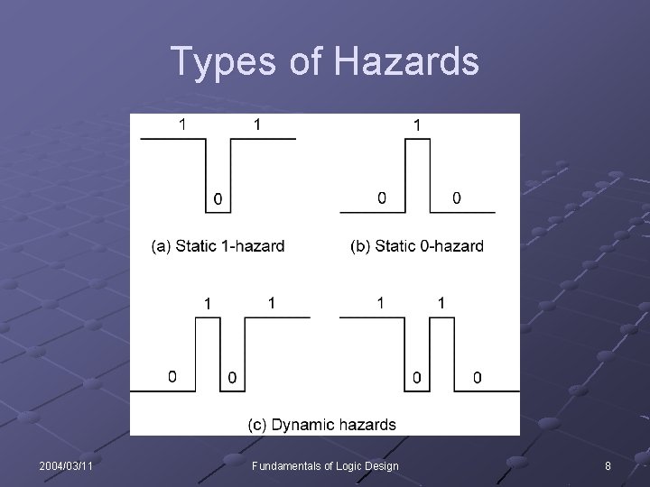
Types of Hazards 2004/03/11 Fundamentals of Logic Design 8
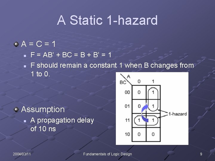
A Static 1 -hazard A=C=1 n n F = AB’ + BC = B + B’ = 1 F should remain a constant 1 when B changes from 1 to 0. Assumption n A propagation delay of 10 ns 2004/03/11 Fundamentals of Logic Design 9
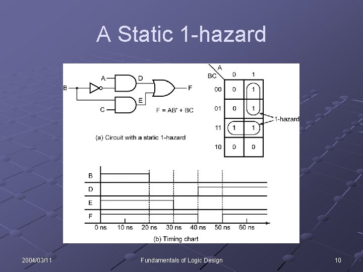
A Static 1 -hazard 2004/03/11 Fundamentals of Logic Design 10
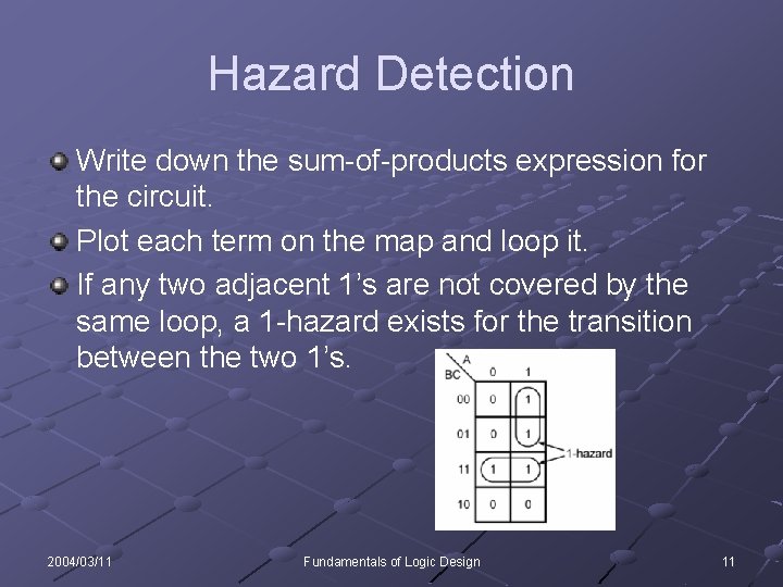
Hazard Detection Write down the sum-of-products expression for the circuit. Plot each term on the map and loop it. If any two adjacent 1’s are not covered by the same loop, a 1 -hazard exists for the transition between the two 1’s. 2004/03/11 Fundamentals of Logic Design 11
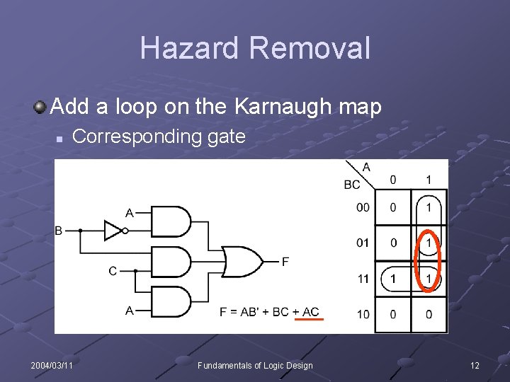
Hazard Removal Add a loop on the Karnaugh map n Corresponding gate 2004/03/11 Fundamentals of Logic Design 12
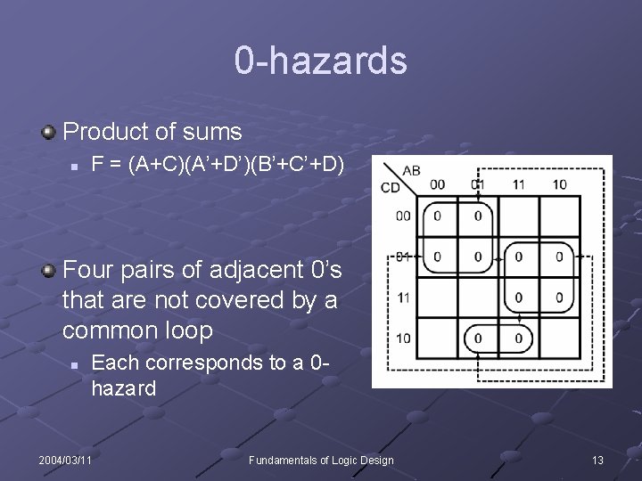
0 -hazards Product of sums n F = (A+C)(A’+D’)(B’+C’+D) Four pairs of adjacent 0’s that are not covered by a common loop n Each corresponds to a 0 hazard 2004/03/11 Fundamentals of Logic Design 13
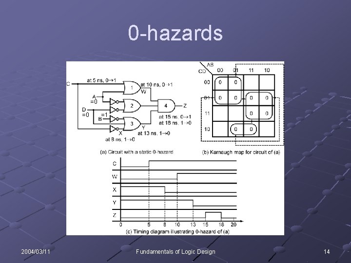
0 -hazards =0 =0 2004/03/11 =1 Fundamentals of Logic Design 14
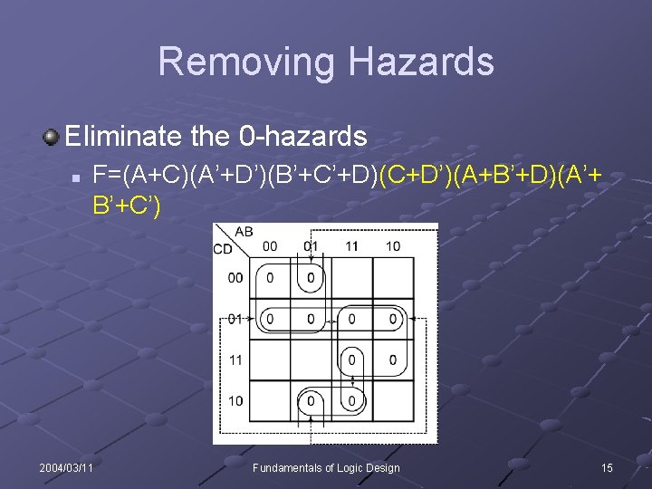
Removing Hazards Eliminate the 0 -hazards n F=(A+C)(A’+D’)(B’+C’+D)(C+D’)(A+B’+D)(A’+ B’+C’) 2004/03/11 Fundamentals of Logic Design 15
Contents 8. 1 Review of Combinational Circuit Design 8. 2 Design Circuits with Limited Gate Fan-In 8. 3 Gate Delays and Timing Diagrams 8. 4 Hazards in Combinational Logic 8. 5 Simulation and Testing of Logic Circuits 2004/03/11 Fundamentals of Logic Design 16
Verification Building a circuit Simulating a circuit on a computer n n n Easier Faster More economical 2004/03/11 Fundamentals of Logic Design 17
Simulation Steps First, specify the circuit component and connections Second, specify the circuit inputs Finally, observe the circuit outputs 2004/03/11 Fundamentals of Logic Design 18
Simulation Two logic values, 0 and 1, are not sufficient n A gate input or output maybe unknown Represented by X n An open circuit, or high impedance (hi-Z) Represented by Z Four-value logic simulator n 0, 1, X, Z 2004/03/11 Fundamentals of Logic Design 19
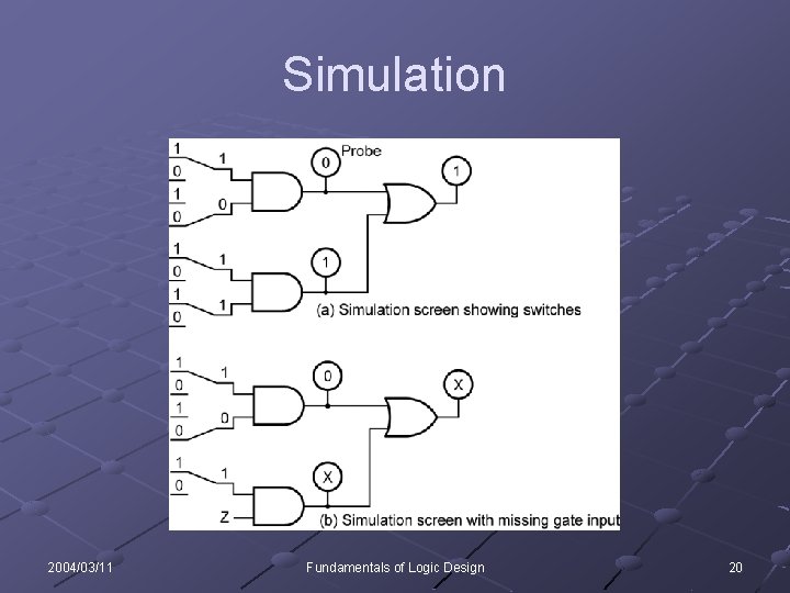
Simulation 2004/03/11 Fundamentals of Logic Design 20
Possible Causes Simulation n Incorrect design Gates connected wrong Wrong input signals to the circuit Built in lab n n Defective gates Defective connecting wires 2004/03/11 Fundamentals of Logic Design 21
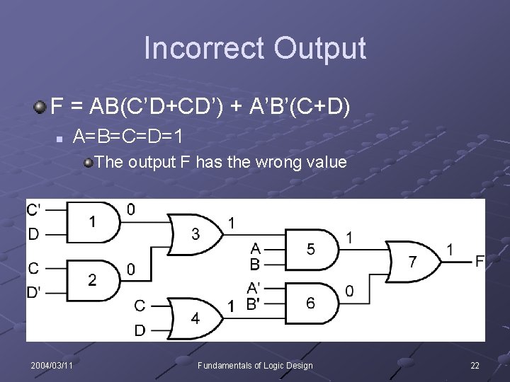
Incorrect Output F = AB(C’D+CD’) + A’B’(C+D) n A=B=C=D=1 The output F has the wrong value 2004/03/11 Fundamentals of Logic Design 22
Homework #2 1. 2. 3. 8. 1 8. 2 8. 3 4. 8. 4 5. 8. 5 Paper Submission, due on April 1, 2004. Late submission will not be accepted. 2004/03/11 Fundamentals of Logic Design 23
- Slides: 23