Unit 5 Programmable Logic and Storage Devices RAMs
Unit 5 Programmable Logic and Storage Devices – RAMs and FPGAs Department of Communication Engineering, NCTU 1
Unit 5 -1 Static Random Access Memory (SRAM) Department of Communication Engineering, NCTU 2
Digital CAS n q q q n Sau-Hsuan Wu Reason for using random access memory (RAM) q n Unit 5 : SRAMs and FPGAs Computers and other digital systems perform operations that retrieve, manipulate, transform and store data Read only memories (ROMs) can not dynamically store data Registers support fast and random storage, but cannot be used for mass storage because they are implemented with FFs and occupy too much physical area RAM is faster and occupies less area than a register file Most RAMs are volatile- the information vanishes after power is removed from the device There are two types of RAMs: static and dynamic q Dynamic RAMs need refresh and static RAMs don’t Department of Communication Engineering, NCTU 3
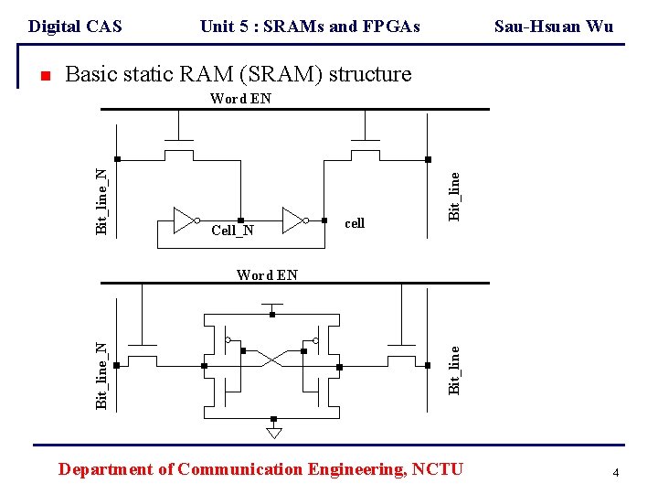
Digital CAS Sau-Hsuan Wu Basic static RAM (SRAM) structure Cell_N cell Bit_line_N Word EN Bit_line_N n Unit 5 : SRAMs and FPGAs Department of Communication Engineering, NCTU 4
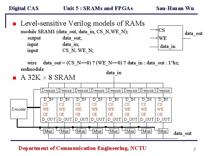
Digital CAS n Unit 5 : SRAMs and FPGAs Sau-Hsuan Wu Level-sensitive Verilog models of RAMs module SRAM 1 (data_out, data_in, CS_N, WE_N); output data_out; input data_in; input CS_N, WE_N; n CS data_out WE data_in wire data_out = (CS_N==0) ? (WE_N==0) ? data_in : data_out : 1’bz; endmodule data_in A 32 K 8 SRAM Demux Demux Decoder D_IN CS WE OE D_OUT D_IN CS WE OE D_OUT Mux Mux Department of Communication Engineering, NCTU data_out 5
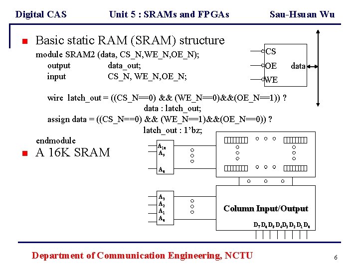
Digital CAS n Unit 5 : SRAMs and FPGAs Basic static RAM (SRAM) structure module SRAM 2 (data, CS_N, WE_N, OE_N); output data_out; input CS_N, WE_N, OE_N; n Sau-Hsuan Wu CS OE data WE wire latch_out = ((CS_N==0) && (WE_N==0)&&(OE_N==1)) ? data : latch_out; assign data = ((CS_N==0) && (WE_N==1)&&(OE_N==0)) ? latch_out : 1’bz; endmodule A A 16 K SRAM 10 A 9 A 0 A 3 A 2 A 1 A 0 Column Input/Output Department of Communication Engineering, NCTU D 7 D 6 D 5 D 4 D 3 D 2 D 1 D 0 6
Unit 5 -3 Altera FPGA Architecture Department of Communication Engineering, NCTU 7
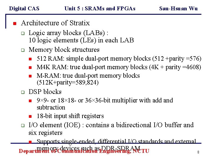
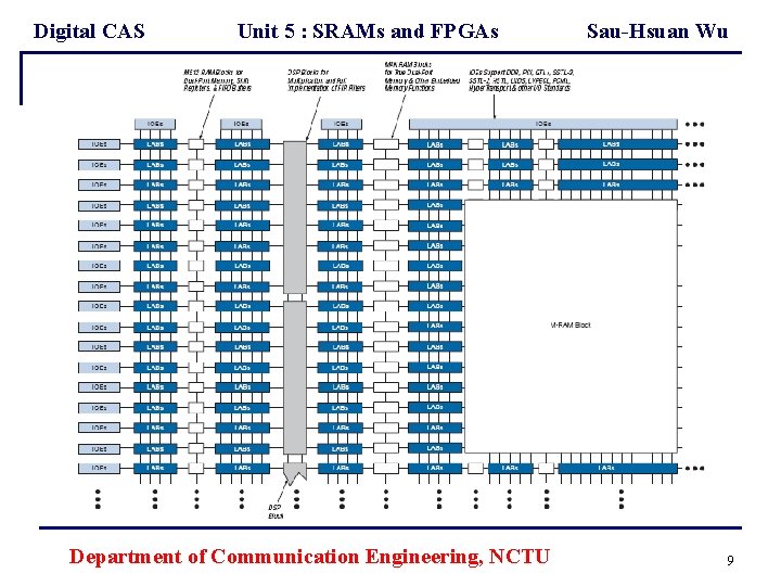
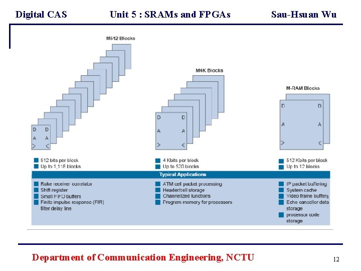
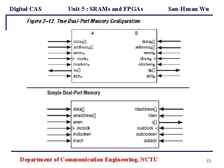
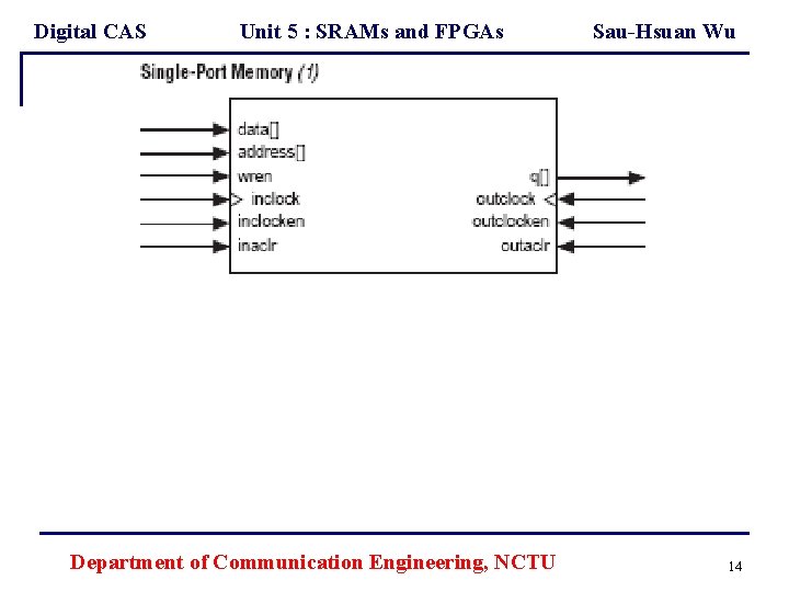
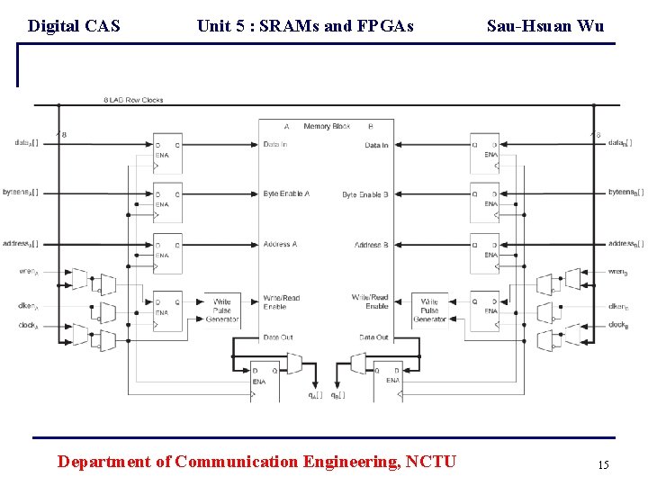
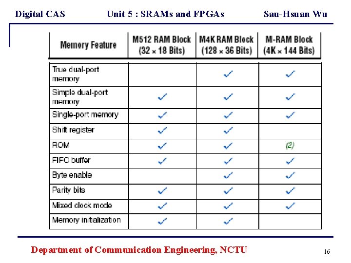
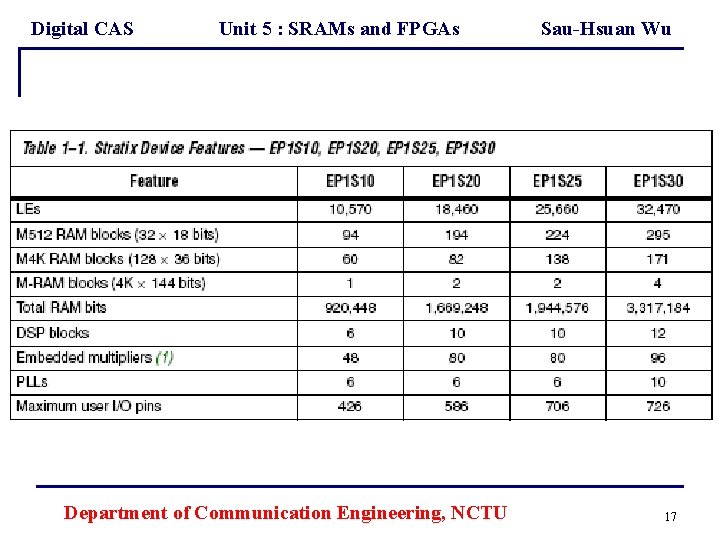
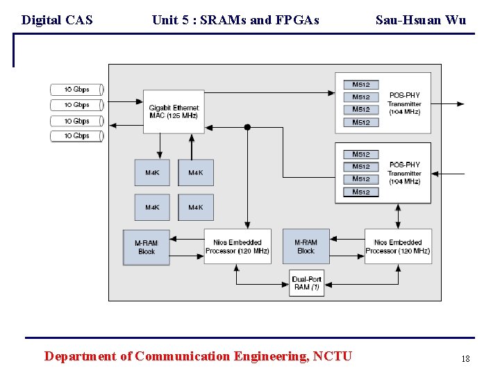
Digital CAS n Unit 5 : SRAMs and FPGAs Sau-Hsuan Wu Architecture of Stratix q q Logic array blocks (LABs) : 10 logic elements (LEs) in each LAB Memory block structures n n n q DSP blocks n n q 512 RAM: simple dual-port memory blocks (512 +parity =576) M 4 K RAM: true dual-port memory blocks (4 K + parity =4608) M-RAM: true dual-port memory blocks (512 K+parity=589, 824) 9× 9 - or 18× 18 - or 36× 36 -bit multiplier with add and subtraction 18 -bit input shift registers I/O element (IOE) : contains a bidirectional I/O buffer and six registers Supports single-ended, differential I/O standards and external memory devices such as. Engineering, DDR-SDRAM Department of Communication NCTU 8 n
Digital CAS Unit 5 : SRAMs and FPGAs Department of Communication Engineering, NCTU Sau-Hsuan Wu 9
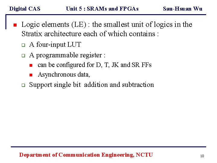
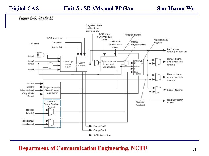
Digital CAS n Unit 5 : SRAMs and FPGAs Sau-Hsuan Wu Logic elements (LE) : the smallest unit of logics in the Stratix architecture each of which contains : q q A four-input LUT A programmable register : n n q can be configured for D, T, JK and SR FFs Asynchronous data, Support single bit addition and subtraction Department of Communication Engineering, NCTU 10
Digital CAS Unit 5 : SRAMs and FPGAs Department of Communication Engineering, NCTU Sau-Hsuan Wu 11
Digital CAS Unit 5 : SRAMs and FPGAs Department of Communication Engineering, NCTU Sau-Hsuan Wu 12
Digital CAS Unit 5 : SRAMs and FPGAs Department of Communication Engineering, NCTU Sau-Hsuan Wu 13
Digital CAS Unit 5 : SRAMs and FPGAs Department of Communication Engineering, NCTU Sau-Hsuan Wu 14
Digital CAS Unit 5 : SRAMs and FPGAs Department of Communication Engineering, NCTU Sau-Hsuan Wu 15
Digital CAS Unit 5 : SRAMs and FPGAs Department of Communication Engineering, NCTU Sau-Hsuan Wu 16
Digital CAS Unit 5 : SRAMs and FPGAs Department of Communication Engineering, NCTU Sau-Hsuan Wu 17
Digital CAS Unit 5 : SRAMs and FPGAs Department of Communication Engineering, NCTU Sau-Hsuan Wu 18
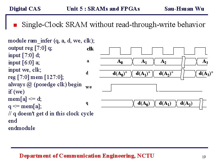
Digital CAS n Unit 5 : SRAMs and FPGAs Sau-Hsuan Wu Single-Clock SRAM without read-through-write behavior module ram_infer (q, a, d, we, clk); output reg [7: 0] q; clk input [7: 0] d; a input [6: 0] a; input we, clk; d reg [7: 0] mem [127: 0]; always @ (posedge clk) begin we if (we) mem[a] <= d; q q <= mem[a]; // q doesn't get d in this clock cycle endmodule A 0 A 1 d(A 0)+ d(A 1)+ d(A 2)+ d(A 0) d(A 1) Department of Communication Engineering, NCTU A 2 A 3 d(A 3)+ d(A 2) 19
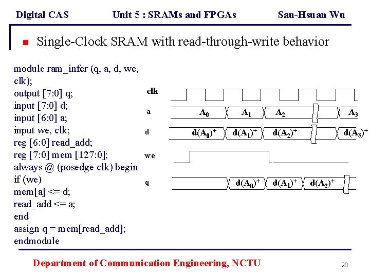
Digital CAS n Unit 5 : SRAMs and FPGAs Sau-Hsuan Wu Single-Clock SRAM with read-through-write behavior module ram_infer (q, a, d, we, clk); clk output [7: 0] q; input [7: 0] d; a input [6: 0] a; input we, clk; d reg [6: 0] read_add; reg [7: 0] mem [127: 0]; we always @ (posedge clk) begin if (we) q mem[a] <= d; read_add <= a; end assign q = mem[read_add]; endmodule A 0 A 1 d(A 0)+ d(A 1)+ d(A 0)+ Department of Communication Engineering, NCTU A 2 A 3 d(A 3)+ d(A 2)+ d(A 1)+ d(A 2)+ 20
Digital CAS Unit 5 : SRAMs and FPGAs Department of Communication Engineering, NCTU Sau-Hsuan Wu 21
Digital CAS Unit 5 : SRAMs and FPGAs Department of Communication Engineering, NCTU Sau-Hsuan Wu 22
Digital CAS Unit 5 : SRAMs and FPGAs Department of Communication Engineering, NCTU Sau-Hsuan Wu 23
Digital CAS Unit 5 : SRAMs and FPGAs Department of Communication Engineering, NCTU Sau-Hsuan Wu 24
Digital CAS Unit 5 : SRAMs and FPGAs Department of Communication Engineering, NCTU Sau-Hsuan Wu 25
Digital CAS Unit 5 : SRAMs and FPGAs Department of Communication Engineering, NCTU Sau-Hsuan Wu 26
Digital CAS Unit 5 : SRAMs and FPGAs Department of Communication Engineering, NCTU Sau-Hsuan Wu 27
Digital CAS Unit 5 : SRAMs and FPGAs Department of Communication Engineering, NCTU Sau-Hsuan Wu 28
Digital CAS Unit 5 : SRAMs and FPGAs Department of Communication Engineering, NCTU Sau-Hsuan Wu 29
Digital CAS Unit 5 : SRAMs and FPGAs Department of Communication Engineering, NCTU Sau-Hsuan Wu 30
Digital CAS Unit 5 : SRAMs and FPGAs Department of Communication Engineering, NCTU Sau-Hsuan Wu 31
Digital CAS Unit 5 : SRAMs and FPGAs Department of Communication Engineering, NCTU Sau-Hsuan Wu 32
Digital CAS Unit 5 : SRAMs and FPGAs Department of Communication Engineering, NCTU Sau-Hsuan Wu 33
Digital CAS Unit 5 : SRAMs and FPGAs Department of Communication Engineering, NCTU Sau-Hsuan Wu 34
Digital CAS Unit 5 : SRAMs and FPGAs Department of Communication Engineering, NCTU Sau-Hsuan Wu 35
Digital CAS Unit 5 : SRAMs and FPGAs Department of Communication Engineering, NCTU Sau-Hsuan Wu 36
Unit 5 -4 Model Simulation Library Department of Communication Engineering, NCTU 37
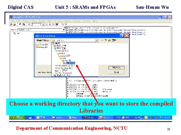
Digital CAS Unit 5 : SRAMs and FPGAs Sau-Hsuan Wu Choose a working directory that you want to store the compiled Libraries Department of Communication Engineering, NCTU 38
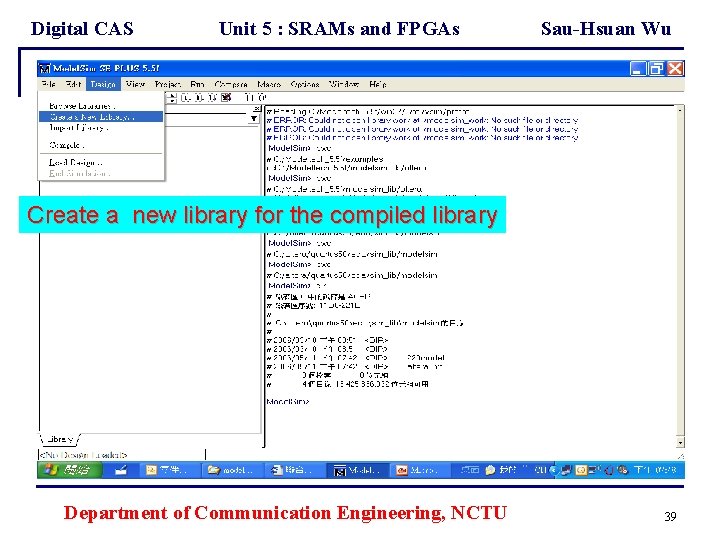
Digital CAS Unit 5 : SRAMs and FPGAs Sau-Hsuan Wu Create a new library for the compiled library Department of Communication Engineering, NCTU 39
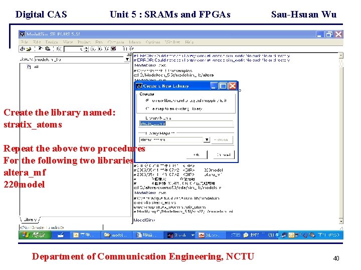
Digital CAS Unit 5 : SRAMs and FPGAs Sau-Hsuan Wu Create the library named: stratix_atoms Repeat the above two procedures For the following two libraries altera_mf 220 model Department of Communication Engineering, NCTU 40
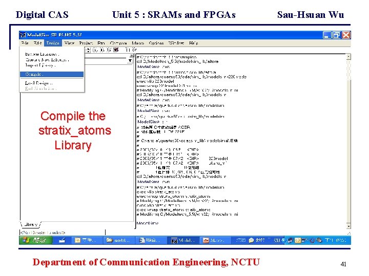
Digital CAS Unit 5 : SRAMs and FPGAs Sau-Hsuan Wu Compile the stratix_atoms Library Department of Communication Engineering, NCTU 41
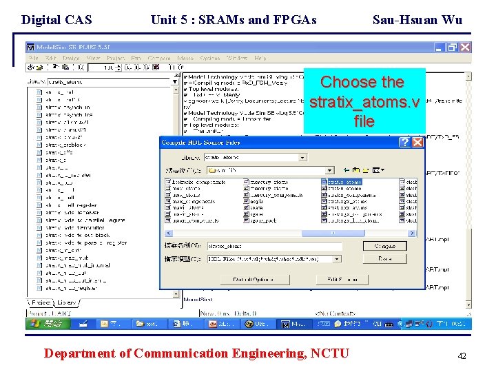
Digital CAS Unit 5 : SRAMs and FPGAs Sau-Hsuan Wu Choose the stratix_atoms. v file Department of Communication Engineering, NCTU 42
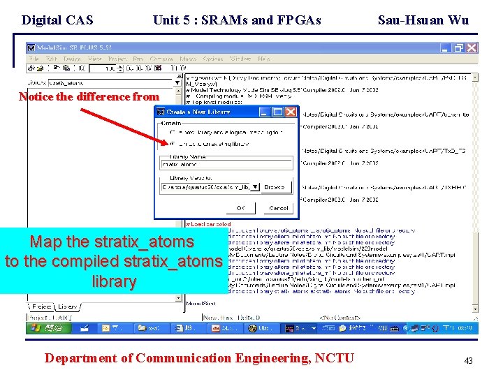
Digital CAS Unit 5 : SRAMs and FPGAs Sau-Hsuan Wu Notice the difference from Map the stratix_atoms to the compiled stratix_atoms library Department of Communication Engineering, NCTU 43
Unit 5 -5 Simulation with Altera mega-functions Department of Communication Engineering, NCTU 44
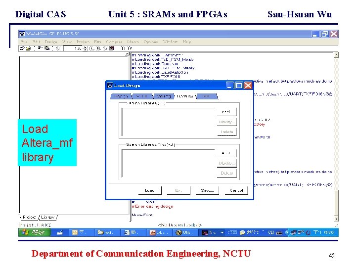
Digital CAS Unit 5 : SRAMs and FPGAs Sau-Hsuan Wu Load Altera_mf library Department of Communication Engineering, NCTU 45
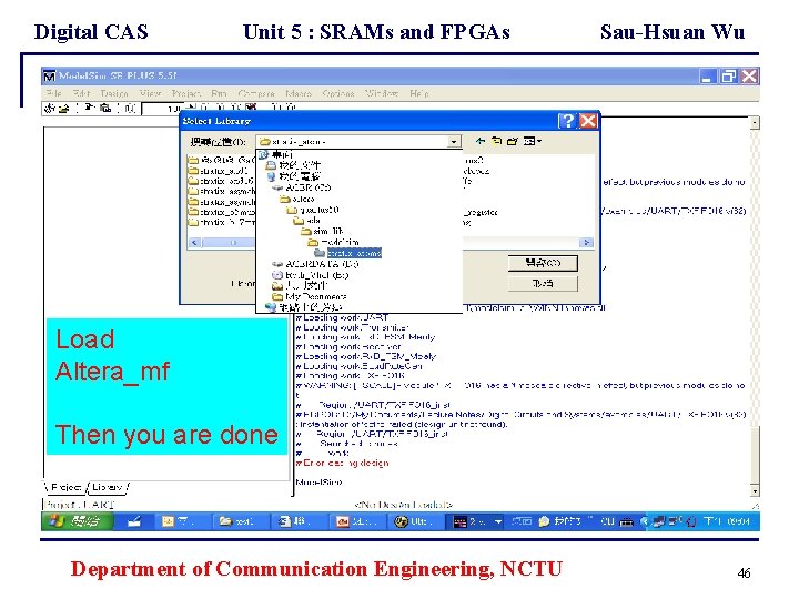
Digital CAS Unit 5 : SRAMs and FPGAs Sau-Hsuan Wu Load Altera_mf Then you are done Department of Communication Engineering, NCTU 46
Unit 5 -5 Post Layout Simulation Department of Communication Engineering, NCTU 47
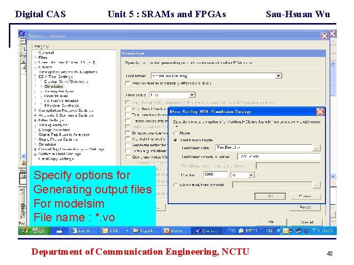
Digital CAS Unit 5 : SRAMs and FPGAs Sau-Hsuan Wu Specify options for Generating output files For modelsim File name : *. vo Department of Communication Engineering, NCTU 48
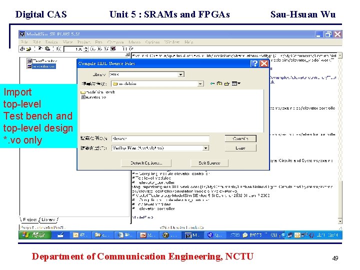
Digital CAS Unit 5 : SRAMs and FPGAs Sau-Hsuan Wu Import top-level Test bench and top-level design *. vo only Department of Communication Engineering, NCTU 49
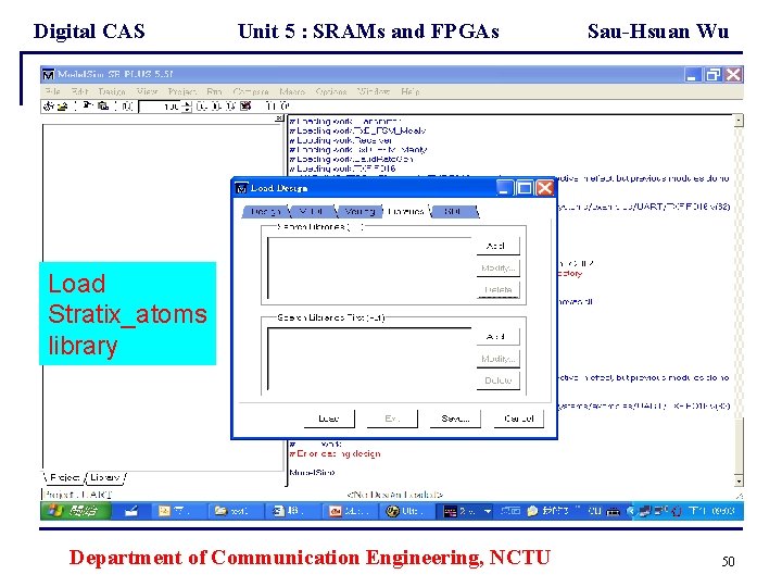
Digital CAS Unit 5 : SRAMs and FPGAs Sau-Hsuan Wu Load Stratix_atoms library Department of Communication Engineering, NCTU 50
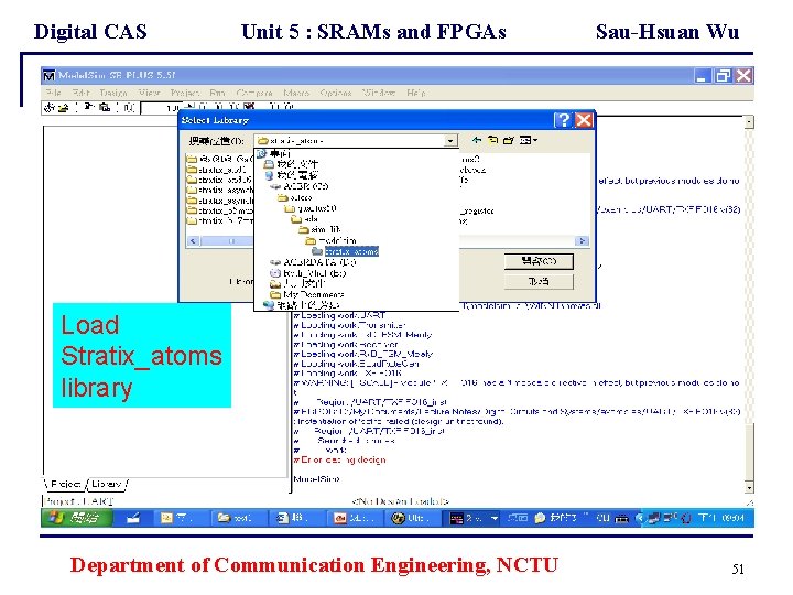
Digital CAS Unit 5 : SRAMs and FPGAs Sau-Hsuan Wu Load Stratix_atoms library Department of Communication Engineering, NCTU 51
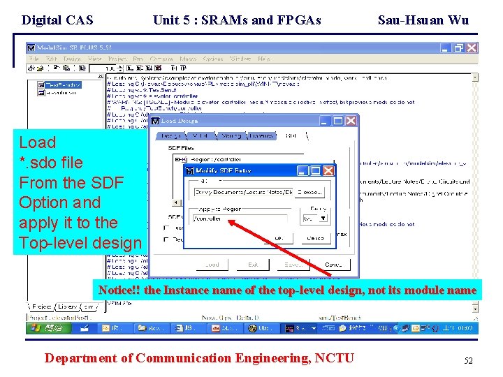
Digital CAS Unit 5 : SRAMs and FPGAs Sau-Hsuan Wu Load *. sdo file From the SDF Option and apply it to the Top-level design Notice!! the Instance name of the top-level design, not its module name Department of Communication Engineering, NCTU 52
- Slides: 52