Unit 5 PPI ADC DAC 8051 Microcontroller Prof


![Microcontroller development tools 1]Simulator, 2]Emulator, 3]Assemblers, 4]Programmers, 5]Cross assembler 3](https://slidetodoc.com/presentation_image_h2/89c161a8fb3bb78d506dfae635826dc9/image-3.jpg "Microcontroller development tools 1]Simulator, 2]Emulator, 3]Assemblers, 4]Programmers, 5]Cross assembler 3")


: These are 8 -bit bi-directional")
: This is used to select the ports.")


![Operation modes: 1] BSR mode, (BIT SET/RESET MODE): • The PORT C can be](https://slidetodoc.com/presentation_image_h2/89c161a8fb3bb78d506dfae635826dc9/image-17.jpg "Operation modes: 1] BSR mode, (BIT SET/RESET MODE): • The PORT C can be")
![• B] MODE 1 : (Input/output with Hand shake) • In this mode,](https://slidetodoc.com/presentation_image_h2/89c161a8fb3bb78d506dfae635826dc9/image-18.jpg "• B] MODE 1 : (Input/output with Hand shake) • In this mode,")


![FORMAT : - 1] BIT SET/RESET MODE: • This is bit set/reset control word](https://slidetodoc.com/presentation_image_h2/89c161a8fb3bb78d506dfae635826dc9/image-22.jpg "FORMAT : - 1] BIT SET/RESET MODE: • This is bit set/reset control word")

![• FORMAT : - 2] I/O MODE: The mode format for I/O as](https://slidetodoc.com/presentation_image_h2/89c161a8fb3bb78d506dfae635826dc9/image-24.jpg "• FORMAT : - 2] I/O MODE: The mode format for I/O as")


![Example : -1 • A] Find the I/O port addresses assigned to ports A,](https://slidetodoc.com/presentation_image_h2/89c161a8fb3bb78d506dfae635826dc9/image-28.jpg "Example : -1 • A] Find the I/O port addresses assigned to ports A,")
![Solution: A]The base address for the 8255 is as follows: • B] The control](https://slidetodoc.com/presentation_image_h2/89c161a8fb3bb78d506dfae635826dc9/image-29.jpg "Solution: A]The base address for the 8255 is as follows: • B] The control")
![C] program: • MOV A, #80 H • MOV DPTR, #4003 H • MOVX](https://slidetodoc.com/presentation_image_h2/89c161a8fb3bb78d506dfae635826dc9/image-30.jpg "C] program: • MOV A, #80 H • MOV DPTR, #4003 H • MOVX")
![Example : -2 • A] Find the I/O port addresses assigned to ports A,](https://slidetodoc.com/presentation_image_h2/89c161a8fb3bb78d506dfae635826dc9/image-31.jpg "Example : -2 • A] Find the I/O port addresses assigned to ports A,")
![Solution: A] Assuming all the unused bits are 0 s, the base port address](https://slidetodoc.com/presentation_image_h2/89c161a8fb3bb78d506dfae635826dc9/image-32.jpg "Solution: A] Assuming all the unused bits are 0 s, the base port address")
![C] program : - • MOV A, #90 H ; (PA=IN, PB=OUT, PC=OUT) •](https://slidetodoc.com/presentation_image_h2/89c161a8fb3bb78d506dfae635826dc9/image-33.jpg "C] program : - • MOV A, #90 H ; (PA=IN, PB=OUT, PC=OUT) •")


 • I/P 0 –I/P 7")


 An analog channel is selected by giving bits to")


- Slides: 53
Unit 5: PPI, & ADC , DAC 8051 Microcontroller Prof. Swati A. Thete J. E. S. I. T. M. R. Nashik 330_02 1
Unit-5 : PPI &ADC, DAC • Microcontroller development tools- study of simulator, emulator, assemblers, programmers, cross assembler for microcontrollers. • Study, interfacing and programming of PPI 8255— mode 0, 1, BSR mode. Interfacing of 8051 with 8255 for expanding of I/O. • Programming and Interfacing of 8051 with 8 bit ADC (0809) and DAC (0808). 2
Microcontroller development tools 1]Simulator, 2]Emulator, 3]Assemblers, 4]Programmers, 5]Cross assembler 3
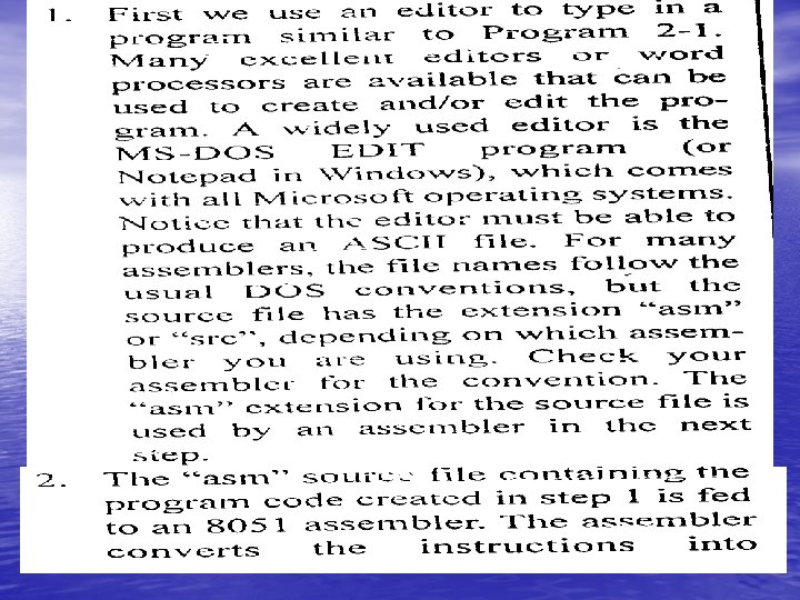
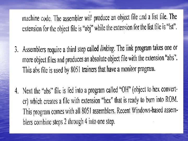
Steps to create a Program
PROGRAMMABLE PERIPHERAL INTERFACE -8255 Features: • It is a programmable device. • It has 24 I/O programmable pins like PA, PB, PC (3 -8 pins). T T L compatible. Improved dc driving capability
Pin Diagram
Function of pins: • Data bus(D 0 -D 7): These are 8 -bit bi-directional buses, connected to 8085 data bus for transferring data. • CS: This is Active Low signal. When it is low, then data is transfer from 8085. • Read: This is Active Low signal, when it is Low read operation will be start. • Write: This is Active Low signal, when it is Low Write operation will be start.
• Address (A 0 -A 1): This is used to select the ports. like this A 1 A 0 Select 0 0 PA 0 1 PB 1 0 PC 1 1 Control reg.
• RESET: This is used to reset the device. That means clear control registers. • PA 0 -PA 7: It is the 8 -bit bi-directional I/O pins used to send the data to peripheral or or to receive the data from peripheral. • PB 0 -PB 7: Similar to PA • PC 0 -PC 7: This is also 8 -bit bidirectional I/O pins. These lines are divided into two groups. 1. PC 0 to PC 3(Lower Groups) 2. PC 4 to PC 7 (Higher groups) These two groups working in separately using 4 data’s.
Block Diagram
Data Bus buffer: • It is a 8 -bit bidirectional Data bus. • Used to interface between 8255 data bus with system bus. • The internal data bus and Outer pins D 0 -D 7 pins are connected in internally. • The direction of data buffer is decided by Read/Control Logic.
Read/Write Control Logic: • This is getting the input signals from control bus and Address bus • Control signal are RD and WR. • Address signals are A 0, A 1, and CS. • 8255 operation is enabled or disabled by CS.
Group A and Group B control: • Group A and B get the Control • • Signal from CPU and send the command to the individual control blocks. Group A send the control signal to port A and Port C (Upper) PC 7 -PC 4. Group B send the control signal to port B and Port C (Lower) PC 3 -PC 0. • PORT A: • This is a 8 -bit buffered I/O latch. • It can be programmed by mode 0 , mode 1, mode 2.
PORT B: • This is a 8 -bit buffer I/O latch. • It can be programmed by mode 0 and mode 1. • PORT C: • This is a 8 -bit Unlatched buffer Input and an Output latch. • It is splitted into two parts. • It can be programmed by bit set/reset operation.
Operation modes: 1] BSR mode, (BIT SET/RESET MODE): • The PORT C can be Set or Reset by sending OUT instruction to the CONTROL registers. 2] I/O MODES: Three sub modes • A] MODE 0(Simple input / Output): • In this mode , port A, port B and port C is used as individually (Simply). • Features: • Outputs are latched , Inputs are buffered not • latched. Ports do not have Handshake or interrupt capability.
• B] MODE 1 : (Input/output with Hand shake) • In this mode, input or output is transferred by hand shaking Signals. Computer DATA BUS STB ACK Printer Busy • Handshaking signals is used to transfer data between whose data transfer speed is not same.
• Example: • The computer send the data to the printer large speed compared to the printer. • When computer send the data according to the printer speed at the time only, printer can accept. • If printer is not ready to accept the data then after sending the data bus , computer uses another handshaking signal to tell printer that valid data is available on the data bus. • Each port uses three lines from port C as handshake signals
MODE 2: bi-directional I/O data transfer: • This mode allows bidirectional data transfer over a single 8 -bit data bus using handshake signals. • This feature is possible only Group A • Port A is working as 8 -biy bidirectional. • PC 3 -PC 7 is used for handshaking purpose. • The data is sent by CPU through this port , when the peripheral request it. • CONTROL WORD FORMATS: • In the INPUT mode , When RESET is High all 24 pins (3 -ports) be a input mode.
• i. e all flip flops are cleared and the interrupts are rest. • This condition is maintained even after RESET goes low. • This can be avoid by writing single control word to the control registers , when required.
FORMAT : - 1] BIT SET/RESET MODE: • This is bit set/reset control word format. D 7 D 6 D 5 D 4 X X X Don’t care D 3 D 2 D 1 D 0 BIT SET/RESET 1=SET 0=RESET Bit select 0 1 2 3 4 5 6 7 0 1 0 1 0 0 1 1 BIT SET/RESET FLAG =0 Active B 0 B 1 B 2
• PC 0 -PC 7 is set or reset as per the status of D 0. • A BSR word is written for each bit • Example: • PC 3 is Set then control register will be 0 XXX 0111. • PC 4 is Reset then control register will be 0 XXX 01000. • X is a don’t care.
• FORMAT : - 2] I/O MODE: The mode format for I/O as shown in figure D 7 D 6 D 5 D 4 D 3 D 2 D 1 D 0 Group A Mode set flag=1=Active Port C Upper 1=Input 0=Output Port B 1=Input 0=Output Mode selection 00=mode 0 01=mode 1 1 x=mode 2 Group B Port C Lower 1=Input 0=Output Port B 1=Input 0=Output Mode selection 0=mode 0 1=mode 1
• The control word for both mode is same. • Bit D 7 is used for specifying whether word loaded in to Bit set/reset mode or Mode definition word. • D 7=1=Mode definition mode. • D 7=0=Bit set/Reset mode.
Interfacing of 8255 with 8051
Interfacing of ADC with 8051 without 8255
Example : -1 • A] Find the I/O port addresses assigned to ports A, B, C, and the control register. • B] Program the 8255 for ports A, B, and C to be output ports. • C] Write a program to send 55 H to all ports continuously.
Solution: A]The base address for the 8255 is as follows: • B] The control byte (word) for all ports as output is 80 H as seen in Example 15 -1.
C] program: • MOV A, #80 H • MOV DPTR, #4003 H • MOVX @DPTR, A • MOV A, #55 H • AGAIN: MOV DPTR, #4000 H • MOVX @DPTR, A • INC DPTR • MOVX @DPTR, A • CPL A • ACALL DELAY • SJMP AGAIN ; control word ; load control reg ; issue control word ; A = 55 H ; PA address ; toggle PA bits ; PB address ; toggle PB bits ; PC address ; toggle PC bits ; toggle bit in reg A ; wait ; continue
Example : -2 • A] Find the I/O port addresses assigned to ports A, B, C, and the control register. • B] Find the control byte for PA = in, PB = out, PC = out. • C] Write a program to get data from PA and send it to both B and C.
Solution: A] Assuming all the unused bits are 0 s, the base port address for 8255 is 1000 H. Therefore we have: • 1000 H PA • 1001 H PB • 1002 H PC • 1003 H Control register B] The control word is 10010000, or 90 H.
C] program : - • MOV A, #90 H ; (PA=IN, PB=OUT, PC=OUT) • MOV DPTR, #1003 H ; load control register • MOVX @DPTR, A ; port address ; issue control • • • word MOV DPTR, #1000 H ; PA address MOVX A, @DPTR ; get data from PA INC DPTR ; PB address MOVX @DPTR, A ; send the data to PB INC DPTR ; PC address MOVX @DPTR, A ; send it also to PC
Data Handling Systems • Both data about the physical world and control signals sent to interact with the physical world are typically "analog" or continuously varying quantities. • In order to use the power of digital electronics, one must convert from analog to digital form on the experimental measurement end and convert from digital to analog form on the control or output end of a laboratory system.
Data Collection and Control
ADC Basic Principle • The basic principle of operation is to use the comparator principle to determine whether or not to turn on a particular bit of the binary number output. • It is typical for an ADC to use a digital -to-analog converter (DAC) to determine of the inputs to the comparator.
ADC Various Approaches • 3 Basic Types • Digital-Ramp ADC • Successive Approximation ADC • Flash ADC
Successive approximation ADC Illustration of 4 -bit SAC with 1 volt step size
ADC 080 x Features • Compatible with 8080 µP • • derivatives—no interfacing logic needed -access time 135 ns Easy interface to all microprocessors, or operates “stand alone” Differential analog voltage inputs Logic inputs and outputs meet both MOS and TTL voltage level specifications Works with 2. 5 V (LM 336) voltage reference On-chip clock generator 0 V to 5 V analog input voltage range with single 5 V supply No zero adjust required
Interfacing Analog to Digital Data Converters (cont. . ) • I/P 0 –I/P 7 : - Analog inputs • ADD A, B, C : - Address lines for selecting analog • • • inputs. O 7 – O 0 : - Digital 8 -bit output with O 7 MSB and O 0 LSB SOC : - Start of conversion signal pin EOC : - End of conversion signal pin OE : - Output latch enable pin, if high enables output CLK : - Clock input for ADC
• Vcc - Supply pins +5 V • GND - GND • Vref + - Reference voltage positive +5 Volts maximum. • Vref_ - Reference voltage negative 0 Volts minimum.
Interfacing of ADC with 8051
Interfacing of ADC with 8051
ALGORITHM FOR PROGRAMMING ADC i) An analog channel is selected by giving bits to A, B, C addresses. ii) ALE(Address Latch Enable) is activated by a low to high pulse in order to latch in the address. iii) SC(Start Conversion) is activated by a low to high pulse in order to start the conversion. iv) If a high to low output is obtained at EOC(End of Conversion), it indicates that the data conversion is finished and the data is ready. v) OE(Output Enable) is activated to read output data from the ADC chip. In order to bring the digital data out of the chip a low to high pulse is is given to the OE pin.
Program • • • MOV DPTR, #2023 MOV A, #90 O/P PORTS MOVX @DPTR, A BEGIN: MOV DPTR, #2022 MOV A, #00 MOVX @DPTR, A MOV A, #0 DH MOV DPTR, #2023 MOVX @DPTR, A MOV A, #0 FH MOVX @DPTR, A ; PA-I/P PORT, PORT B, C- ; Select CH-0 ; Set PC 6 (OE) ; SET SOC
• LCALL DELAY • MOV A, #0 EH • MOVX @DPTR, A • MOV A, #0 CH • MOVX @DPTR, A • MOV DPTR, #2020 • BACK: MOVX A, @DPTR • JB 0 E 7, BACK • MOV DPTR, #2020 • REP: MOVX A, @DPTR • ANL A, #80 H • JNB 0 E 7, REP • MOV A, #0 DH • MOV DPTR, #2023 • MOVX @DPTR, A
• • • MOV DPTR, #2020 MOVX A, @DPTR MOV DPTR, #9000 H; Read the digital output from this address MOVX @DPTR, A SJMP BEGIN DELAY: MOV R 3, #30 H AGAIN: MOV R 4, #FFH BACK: NOP DJNZ R 4, BACK DJNZ R 3, AGAIN RET
Digital-to-Analog Conversion • 2 Basic Approaches – Weighted Summing Amplifier – R-2 R Network Approach
Algorithm for interface 8051 with DAC: • Step 1: Connect the P 1 of 8051 with D 0 -D 7 pins of DAC • Step 2: Give +5 v to VCC & Vref of DAC Step 3: Connect -12 v to VEE of DAC • Step 4: Connect OPAMP to OUT pin of the DAC With 5 K resistor • Step 5: Connect the oscilloscope to the OPAMP to View the output
Interfacing of DAC with 8051
Typical Application
8051 assembly code to generate triangular wave • ORG 0 CLR A UP: INC A MOV P 2, A CJNE A, #0 FFH, UP LCALL DELAY DOWN: DEC A MOV P 2, A CJNE A, #00, DOWN LCALL DELAY SJMP UP END
Thank you Q&A