Unit 4 Memory System Design Memory System There



- Slides: 103

Unit -4 Memory System Design

Memory System • There are two basic parameters that determine Memory systems Performance 1. Access Time: Time for a processor request to be transmitted to the memory system, access a datum and return it back to the processor. ( Depends on physical parameter like bus delay, chip delay etc. ) 2. Memory Bandwidth: Ability of the memory to respond to requests per unit of time. ( depends on memory system organization, No of memory modules etc.

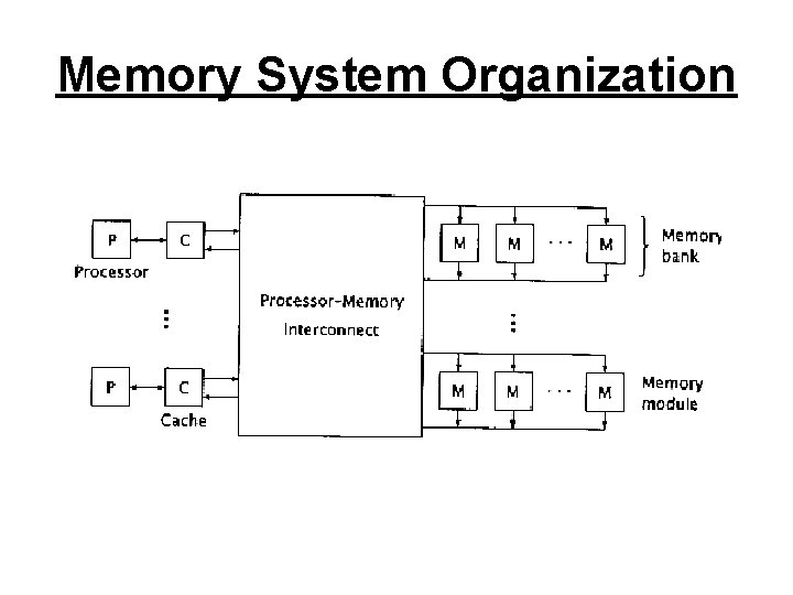
Memory System Organization

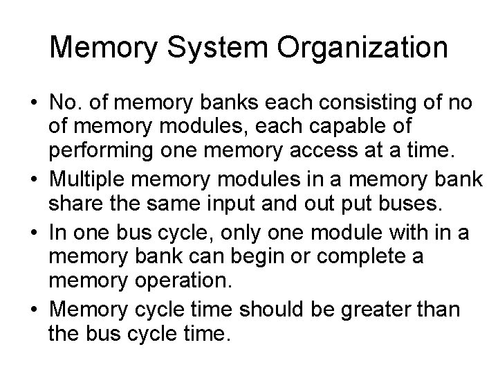
Memory System Organization • No. of memory banks each consisting of no of memory modules, each capable of performing one memory access at a time. • Multiple memory modules in a memory bank share the same input and out put buses. • In one bus cycle, only one module with in a memory bank can begin or complete a memory operation. • Memory cycle time should be greater than the bus cycle time.

Memory System Organization • In systems with multiple processors or with complex single processors, multiple requests may occur at the same time causing bus or network congestion. • Even in single processor system requests arising from different buffered sources may request access to same memory module resulting in memory systems contention degrading the bandwidth.

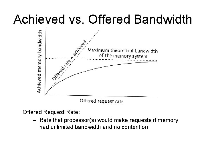
Memory System Organization • The maximum theoretical bandwidth of the memory system is given by the number of memory modules divided by memory cycle time. • The Offered Request Rate is the rate at which processor would be submitting memory requests if memory had unlimited bandwidth. • Offered request rate and maximum memory bandwidth determine maximum Achieved Memory Bandwidth

Achieved vs. Offered Bandwidth Offered Request Rate: – Rate that processor(s) would make requests if memory had unlimited bandwidth and no contention

Memory System Organization • The offered request rate is not dependent on organization of memory system. • It depends on processor architecture and instruction set etc. • The analysis and modeling of memory system depends on no of processors that request service from common shared memory system. • For this we use a model where n simple processors access m independent modules.

Memory System Organization • Contention develops when multiple processors access the same module. • A single pipelined processor making n requests to memory system during a memory cycle resembles the n processor m modules memory system.

The Physical Memory Module • Memory module has two important parameters – Module Access Time: Amount of time to retrieve a word into output memory buffer of the module, given a valid address in its address register. – Module Cycle Time: Minimum time between requests directed at the same module. Memory access Time is the total time for the processor to access a word in memory. In a large interleaved memory system it includes module access time plus transit time on bus, bus accessing overhead, error detection and correction delay etc.

Semiconductor Memories • Semiconductor memories fall into two categories. – Static RAM or SRAM – Dynamic RAM or DRAM The data retention methods of SRAM are static where as for DRAM its Dynamic. Data in SRAM remains in stable state as long as power is on. Data in DRAM requires to be refreshed at regular time intervals.

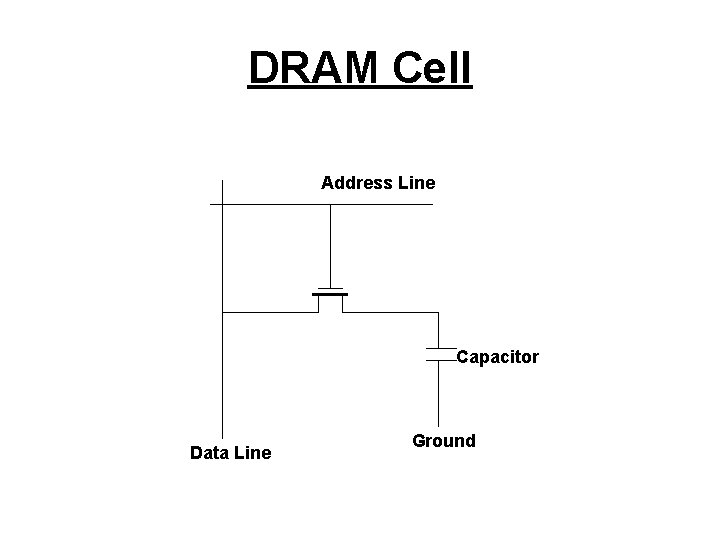
DRAM Cell Address Line Capacitor Data Line Ground

SRAM Vs DRAM • SRAM cell uses 6 transistor and resembles flip flops in construction. • Data information remains in stable state as long as power is on. • SRAM is much less dense than DRAM but has much faster access and cycle time. • In a DRAM cell data is stored as charge on a capacitor which decays with time requiring periodic refresh. This increases access and cycle times

SRAM Vs DRAM • DRAM cells constructed using a capacitor controlled by single transistor offer very high storage density. • DRAM uses destructive read out process so data readout must be amplified and subsequently written back to the cell • This operation can be combined with periodic refreshing required by DRAMS. • The main advantage of DRAM cell is its small size, offering very high storage density and low power consumption.

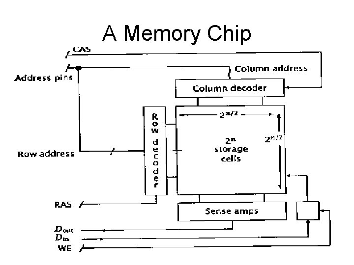
Memory Module • Memory modules are composed of DRAM chips. • DRAM chip is usually organized as 2 n X 1 bit, where n is an even number. • Internally chip is a two dimensional array of memory cells consisting of rows and columns. • Half of memory address is used to specify a row address, (one of 2 n/2 row lines) • Other half is similarly used to specify one of 2 n/2 column lines.

A Memory Chip

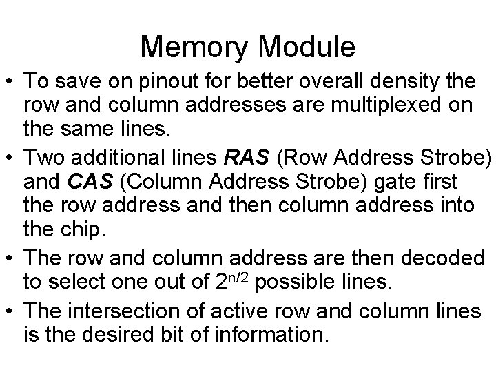
Memory Module • To save on pinout for better overall density the row and column addresses are multiplexed on the same lines. • Two additional lines RAS (Row Address Strobe) and CAS (Column Address Strobe) gate first the row address and then column address into the chip. • The row and column address are then decoded to select one out of 2 n/2 possible lines. • The intersection of active row and column lines is the desired bit of information.

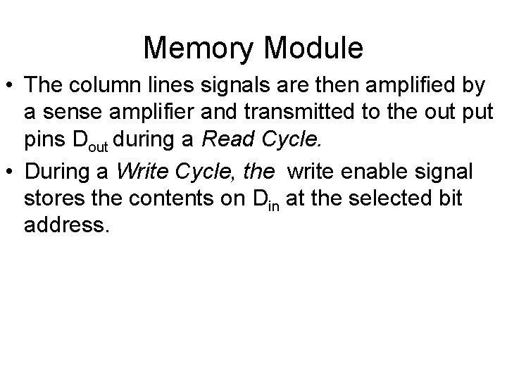
Memory Module • The column lines signals are then amplified by a sense amplifier and transmitted to the out pins Dout during a Read Cycle. • During a Write Cycle, the write enable signal stores the contents on Din at the selected bit address.

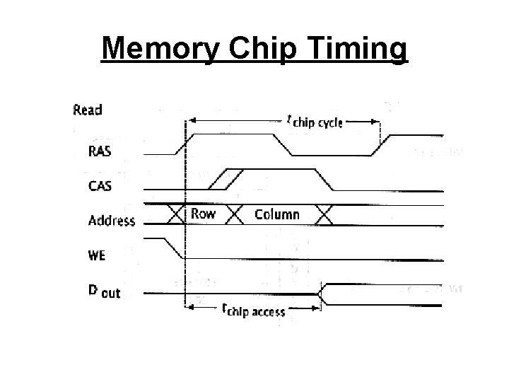
Memory Chip Timing

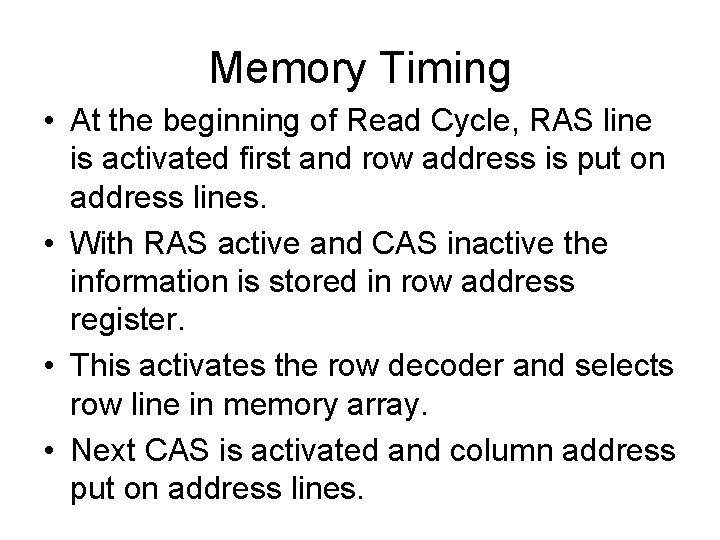
Memory Timing • At the beginning of Read Cycle, RAS line is activated first and row address is put on address lines. • With RAS active and CAS inactive the information is stored in row address register. • This activates the row decoder and selects row line in memory array. • Next CAS is activated and column address put on address lines.

Memory Timing • CAS gates the column address into column address register. • The column address decoder then selects a column line. • Desired data bit lies at the intersection of active row and column address lines. • During a Read Cycle the Write Enable is inactive ( low) and the output line D out is at high impedance state until its activated high or low depending on contents of selected location.

Memory Timing • Time from beginning of RAS until the data output line is activated is called the chip access time. ( t chip access). • T chip cycle is the time required by the row and column address lines to recover before next address can be entered and read or write process initiated. • This is determined by the amount of time that RAS line is active and minimum amount of time that RAS must remain inactive to let chip and sense amplifiers to fully recover for next operation.

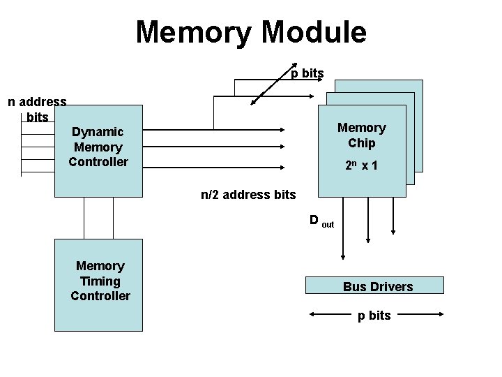
Memory Module • In addition to memory chips a memory module consists of a Dynamic Memory Controller and a Memory Timing Controller to provide following functions. – Multiplex of n address bits into row and column address. – Creation of correct RAS and CAS signal lines at the appropriate time – Provide timely refresh to memory system.

Memory Module p bits n address bits Memory Chip Dynamic Memory Controller 2 n x 1 n/2 address bits D out Memory Timing Controller Bus Drivers p bits

Memory Module • As memory read operation is completed the data out signals are directed at bus drivers which interface with memory bus, common to all the memory modules. • The access and cycle time of module differ from chip access and cycle times. • Module access time includes the delays due to dynamic memory controller, chip access time and delay in transitioning through the output bus drivers.

Memory Module • So in a memory system we have three access and cycle times. – Chip access and Chip cycle time – Module access and Module Cycle time – Memory (System) access and cycle time. (Each lower item includes the upper items)

Memory Module • Two important features found on number of memory chips are used to improve the transfer rates of memory words. – Nibble Mode – Page Mode

Nibble Mode • A single address is presented to memory chip and the CAS line is toggled repeatedly. • Chip interprets this CAS toggling as mod 2 w progression of low order column addresses. • For w=2, four sequential words can be accessed at a higher rate from the memory chip. [00] ---[01]----[10]-----[11]

Page Mode • A single row is selected and non sequential column addresses may be entered at a higher rate by repeatedly activating the CAS line • Its slower than nibble mode but has greater flexibility in addressing multiple words in a single address page • Nibble mode usually refers to access of four consecutive words. Chips that feature retrieval of more than four consecutive words call this feature as fast page mode

Error Detection and Correction • DRAM cells using very high density have very small size. • Each cell thus carries very small amount of charge to determine data state. • Chances of corruptions are very high due to environmental perturbations, static electricity etc. • Error detection and correction is thus intrinsic part of memory system design.

Error Detection and Correction • Simplest type of error detection is Parity. • A bit called parity bit is added to each memory word, which ensures that the sum of the number of 1’s in the word is even (or odd). • If a single error occurs to any bit in the word, the sum modulo 2 of the number of 1’s in the word is inconsistent with parity assumption and word is known to have been corrupted.

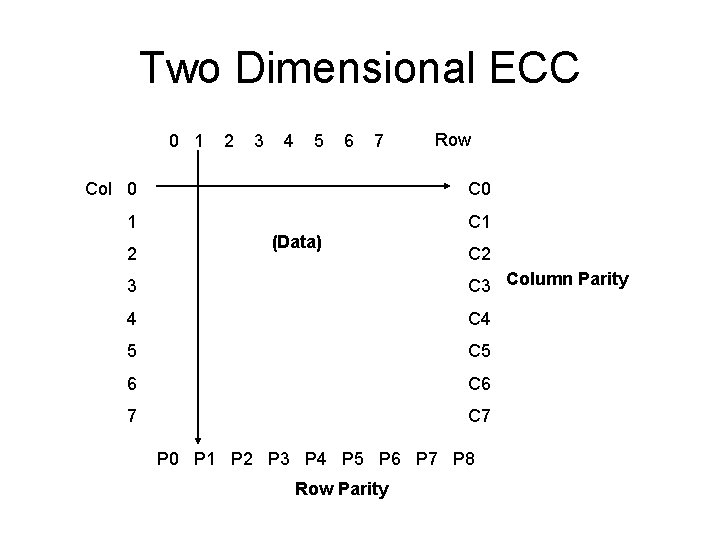
Error Detection and Correction • Most modern memories incorporate hardware to automatically correct single errors ( ECC – error correcting codes) • The simplest code of this type might consist of a geometric block code • The message bits to be checked are arranged in a roughly square pattern and each column and row is augmented with a parity bit. • If a row and column indicate a flaw when decoded at receiver end, then fault lies at the intersection bit which can be simply inverted for error correction.

Two Dimensional ECC 0 1 2 3 4 5 6 7 Row Col 0 C 0 1 C 1 2 (Data) C 2 3 Column Parity 4 C 4 5 C 5 6 C 6 7 C 7 P 0 P 1 P 2 P 3 P 4 P 5 P 6 P 7 P 8 Row Parity

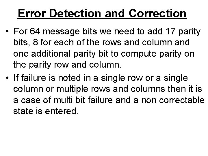
Error Detection and Correction • For 64 message bits we need to add 17 parity bits, 8 for each of the rows and column and one additional parity bit to compute parity on the parity row and column. • If failure is noted in a single row or a single column or multiple rows and columns then it is a case of multi bit failure and a non correctable state is entered.

Achieved Memory Bandwidth • Two factors have substantial effect on achieved memory bandwidth. – Memory Buffers : Buffering should be provided for memory requests in the processor or memory system until the memory reference is complete. This maximizes requests made by the processor resulting in possible increase in achieved bandwidth. – Partitioning of Address Space: The memory space should be partitioned in such a manner that memory references are equally distributed across memory modules.

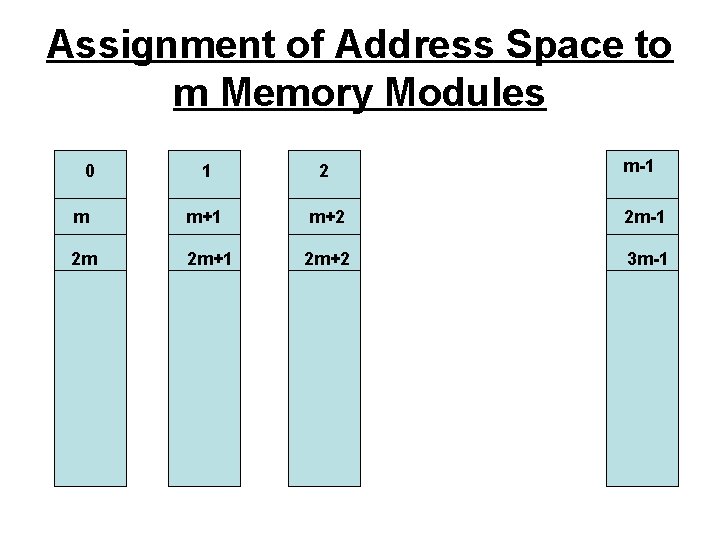
Assignment of Address Space to m Memory Modules 0 m-1 1 2 m m+1 m+2 2 m-1 2 m 2 m+1 2 m+2 3 m-1

Interleaved Memory System • Partitioning memory space in m memory modules is based on the premise that successive references tend to be successive memory locations. • Successive memory locations are assigned to distinct memory modules. • For m memory modules an address x is assigned to a module x mod m. • This partitioning strategy is termed interleaved memory system and no of modules m is the degree of interleaving.

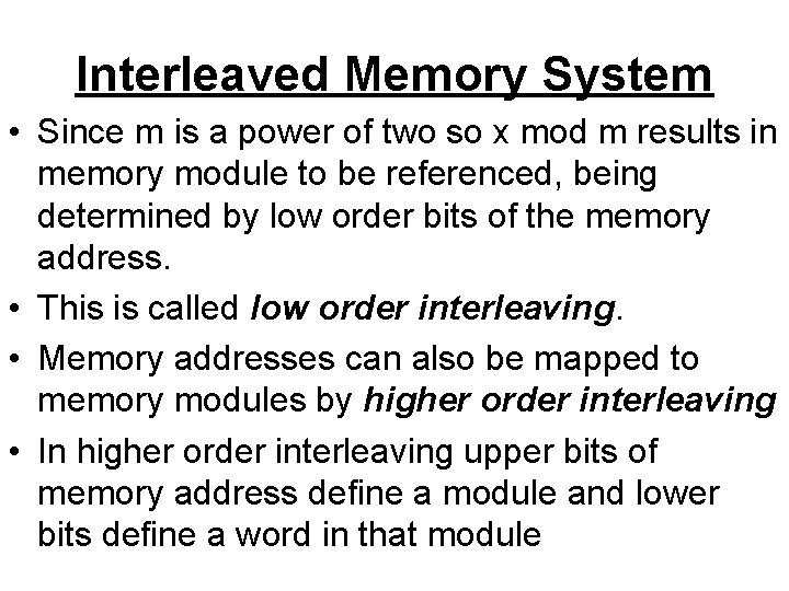
Interleaved Memory System • Since m is a power of two so x mod m results in memory module to be referenced, being determined by low order bits of the memory address. • This is called low order interleaving. • Memory addresses can also be mapped to memory modules by higher order interleaving • In higher order interleaving upper bits of memory address define a module and lower bits define a word in that module

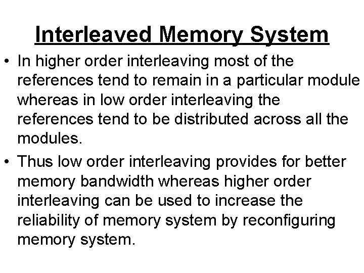
Interleaved Memory System • In higher order interleaving most of the references tend to remain in a particular module whereas in low order interleaving the references tend to be distributed across all the modules. • Thus low order interleaving provides for better memory bandwidth whereas higher order interleaving can be used to increase the reliability of memory system by reconfiguring memory system.

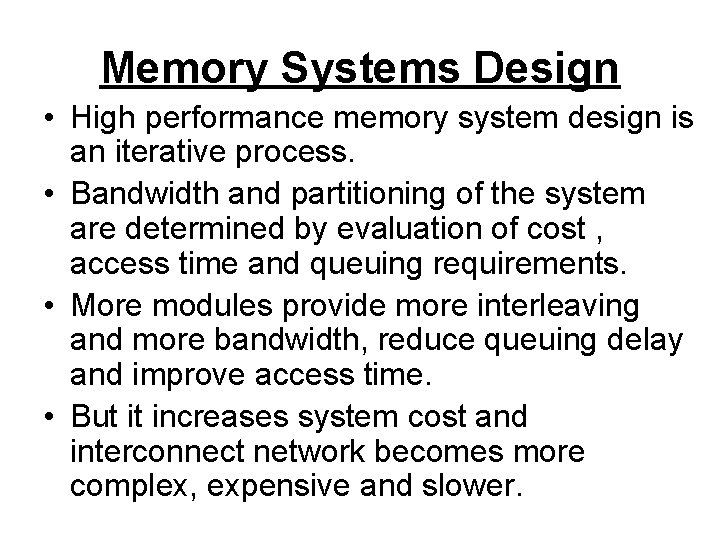
Memory Systems Design • High performance memory system design is an iterative process. • Bandwidth and partitioning of the system are determined by evaluation of cost , access time and queuing requirements. • More modules provide more interleaving and more bandwidth, reduce queuing delay and improve access time. • But it increases system cost and interconnect network becomes more complex, expensive and slower.

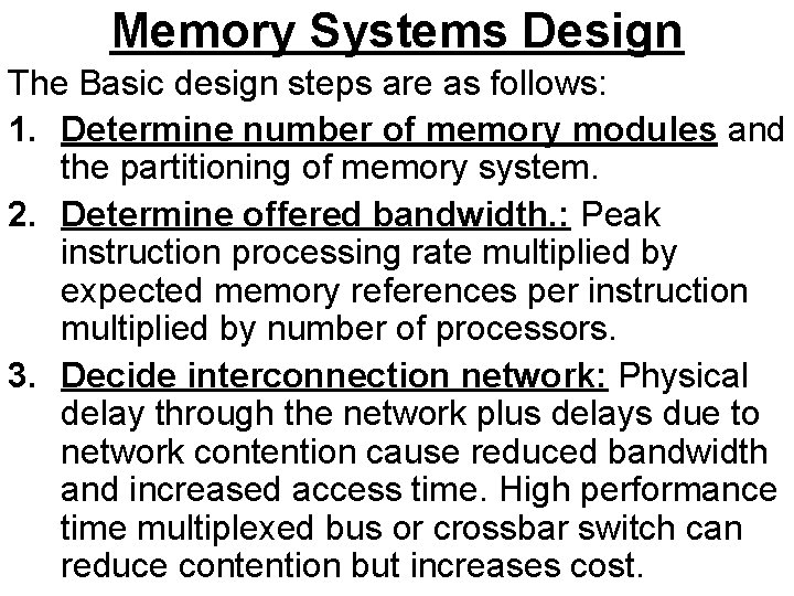
Memory Systems Design The Basic design steps are as follows: 1. Determine number of memory modules and the partitioning of memory system. 2. Determine offered bandwidth. : Peak instruction processing rate multiplied by expected memory references per instruction multiplied by number of processors. 3. Decide interconnection network: Physical delay through the network plus delays due to network contention cause reduced bandwidth and increased access time. High performance time multiplexed bus or crossbar switch can reduce contention but increases cost.

Memory Systems Design 4. Assess Referencing Behavior: Program behavior in its sequence of requests to memory can be - Purely sequential: each request follows a sequence. - Random: requests uniformly distributed across modules. -Regular: Each access separated by a fixed number ( Vector or array references) Random request pattern is commonly used in memory systems evaluation.

Memory Systems Design 5. Evaluate memory model: Assessment of Achieved Bandwidth and actual memory access time and the queuing required in the memory system in order to support the achieved bandwidth.

Memory Models Nature of Processor: • Simple Processor: Makes a single request and waits for response from memory. • Pipelined Processor: Makes multiple requests for various buffers in each memory cycle • Multiple Processors: Each requesting once every memory cycle. Single processor with n requests per memory cycle is asymptotically equivalent to n processors each requesting once every memory cycle.

Memory Models Achieved Bandwidth: Bandwidth available from memory system. B (m) or B (m, n): Number of requests that are serviced each module service time Ts = Tc , (m is the number of modules and n is number of requests each cycle. ) B (w) : Number of requests serviced per second. B (w) = B (m) / Ts

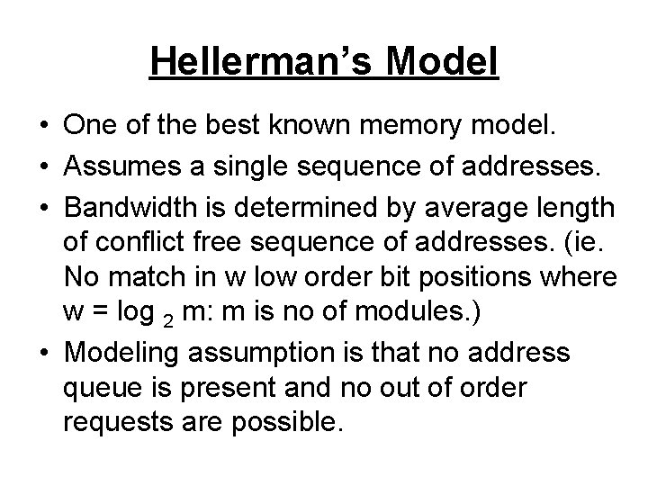
Hellerman’s Model • One of the best known memory model. • Assumes a single sequence of addresses. • Bandwidth is determined by average length of conflict free sequence of addresses. (ie. No match in w low order bit positions where w = log 2 m: m is no of modules. ) • Modeling assumption is that no address queue is present and no out of order requests are possible.

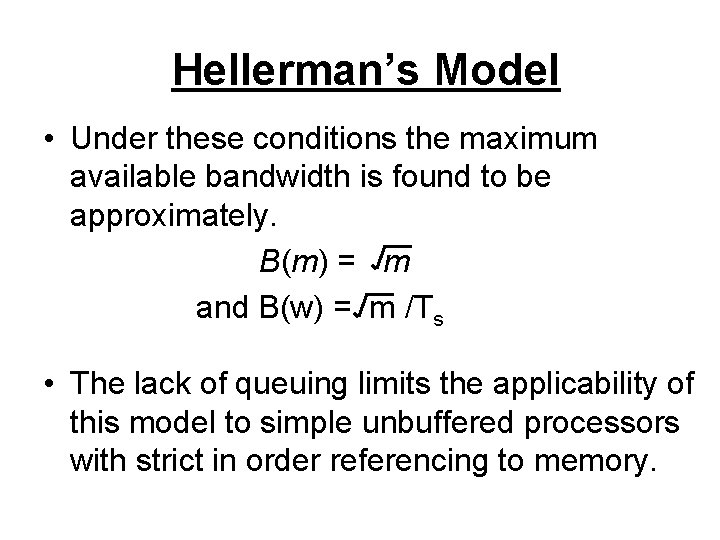
Hellerman’s Model • Under these conditions the maximum available bandwidth is found to be approximately. B(m) = m and B(w) = m /Ts • The lack of queuing limits the applicability of this model to simple unbuffered processors with strict in order referencing to memory.

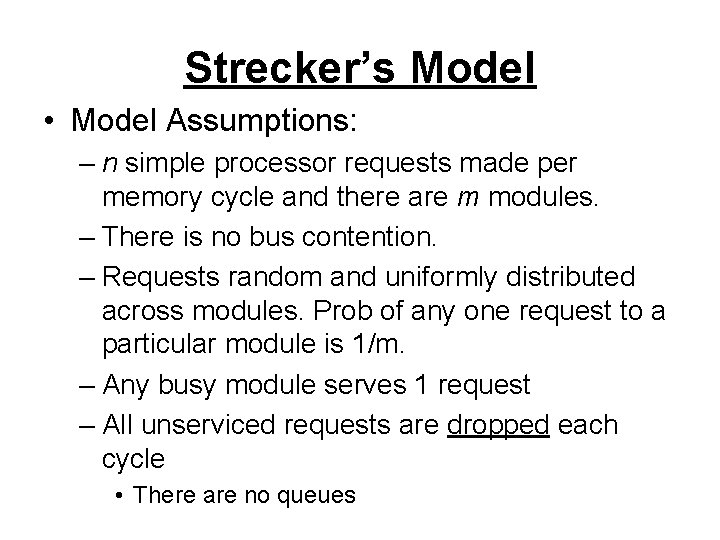
Strecker’s Model • Model Assumptions: – n simple processor requests made per memory cycle and there are m modules. – There is no bus contention. – Requests random and uniformly distributed across modules. Prob of any one request to a particular module is 1/m. – Any busy module serves 1 request – All unserviced requests are dropped each cycle • There are no queues

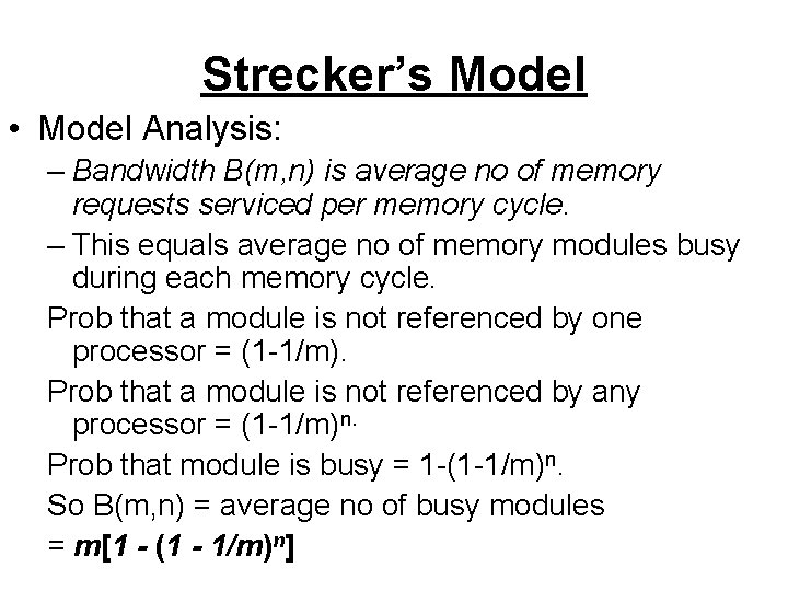
Strecker’s Model • Model Analysis: – Bandwidth B(m, n) is average no of memory requests serviced per memory cycle. – This equals average no of memory modules busy during each memory cycle. Prob that a module is not referenced by one processor = (1 -1/m). Prob that a module is not referenced by any processor = (1 -1/m)n. Prob that module is busy = 1 -(1 -1/m)n. So B(m, n) = average no of busy modules = m[1 - (1 - 1/m)n]

Strecker’s Model • Achieved memory bandwidth is less than theoretical due to contention. • Neglecting congestion carried over from previous cycles results in calculated bandwidth to be still higher.

Processor Memory Modeling Using Queuing Theory • Most real life processors make buffered requests to memory. • Whenever requests are buffered the effect of contention and resulting delays are reduced. • More powerful tools like Queuing Theory are needed to accurately model processor –memory relationships which can incorporate buffered requests.

Queuing Theory • A statistical tool applicable to general environments where some requestors desire service from a common server. • The requestors are assumed to be independent from each other and they make requests based on certain request probability distribution function. • Server is able to process requests one at a time , each independently of others, except that service time is distributed according to server probability distribution function.

Queuing Theory • The mean of the arrival or request rate (measured in items per unit of time) is called λ. • The mean of service rate distribution is called μ. ( Mean service time Ts = 1/μ ) • The ratio of arrival rate (λ) and service rate (μ) is called the utilization or occupancy of the system and is denoted by ρ. (λ/μ) • Standard deviation of service time (Ts) distribution is called σ.

Queuing Theory • Queue models are categorized by the triple. Arrival Distribution / Service Distribution / Number of servers. • Terminology used to indicate particular probability distribution. – M: Poisson / Exponential – MB: Binomial – D : Constant – G: General c=1 c=0 c= arbitrary

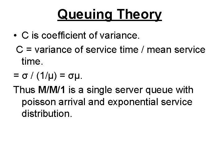
Queuing Theory • C is coefficient of variance. C = variance of service time / mean service time. = σ / (1/μ) = σμ. Thus M/M/1 is a single server queue with poisson arrival and exponential service distribution.

Queue Properties N Size Q ρ μ Ts Tw T Time

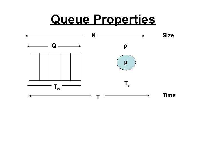
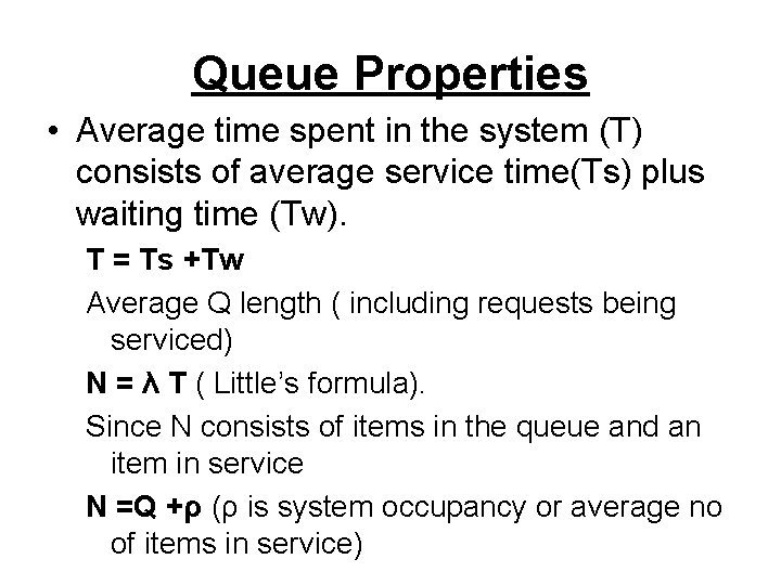
Queue Properties • Average time spent in the system (T) consists of average service time(Ts) plus waiting time (Tw). T = Ts +Tw Average Q length ( including requests being serviced) N = λ T ( Little’s formula). Since N consists of items in the queue and an item in service N =Q +ρ (ρ is system occupancy or average no of items in service)

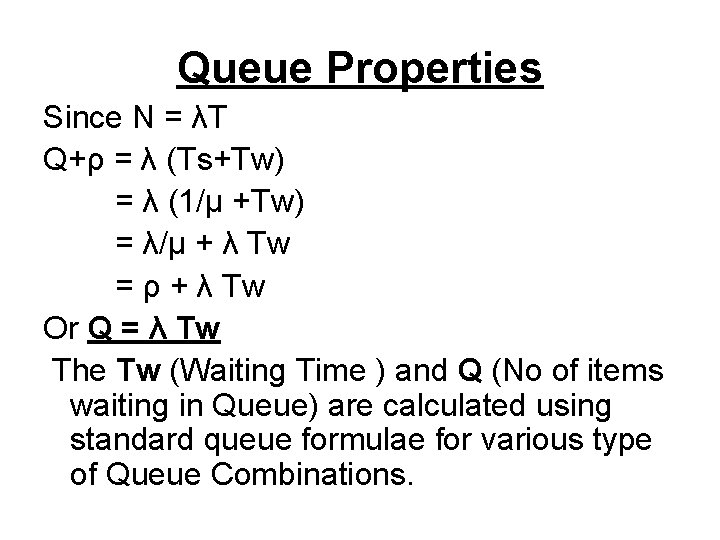
Queue Properties Since N = λT Q+ρ = λ (Ts+Tw) = λ (1/µ +Tw) = λ/µ + λ Tw = ρ + λ Tw Or Q = λ Tw The Tw (Waiting Time ) and Q (No of items waiting in Queue) are calculated using standard queue formulae for various type of Queue Combinations.

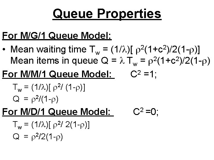
Queue Properties For M/G/1 Queue Model: • Mean waiting time Tw = (1/ )[ 2(1+c 2)/2(1 - )] Mean items in queue Q = Tw = 2(1+c 2)/2(1 - ) For M/M/1 Queue Model: C 2 =1; Tw = (1/ )[ 2/ (1 - )] Q = 2/(1 - ) For M/D/1 Queue Model: Tw = (1/ )[ 2/ 2(1 - )] Q = 2/2(1 - ) C 2 =0;

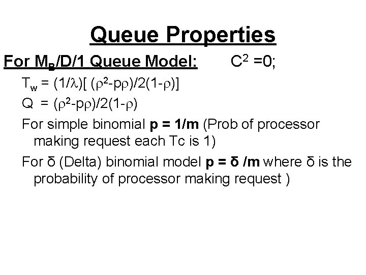
Queue Properties For MB/D/1 Queue Model: C 2 =0; Tw = (1/ )[ ( 2 -p )/2(1 - )] Q = ( 2 -p )/2(1 - ) For simple binomial p = 1/m (Prob of processor making request each Tc is 1) For δ (Delta) binomial model p = δ /m where δ is the probability of processor making request )

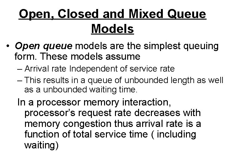
Open, Closed and Mixed Queue Models • Open queue models are the simplest queuing form. These models assume – Arrival rate Independent of service rate – This results in a queue of unbounded length as well as a unbounded waiting time. In a processor memory interaction, processor’s request rate decreases with memory congestion thus arrival rate is a function of total service time ( including waiting)

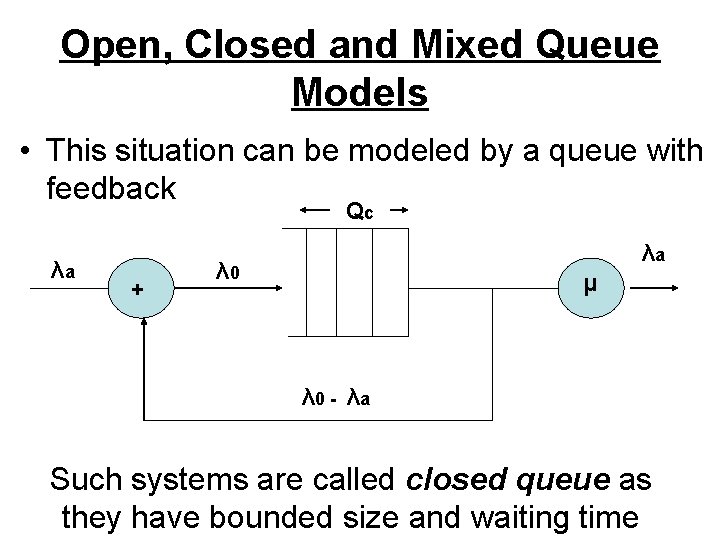
Open, Closed and Mixed Queue Models • This situation can be modeled by a queue with feedback Qc λa + λa λ 0 µ λ 0 - λa Such systems are called closed queue as they have bounded size and waiting time

Open, Closed and Mixed Queue Models • Certain systems can behave as open queue up to a certain queue size and then behave as closed queues. • Such systems are called Mixed Queue systems

Open Queue ( Flores) Memory Model • Open queue model is not very suitable for processor memory interaction but its most simple model and can be used as initial guess to partition of memory modules. • This model was originally proposed by flores using M/D/1 queue but MB/D/1 queue is more appropriate.

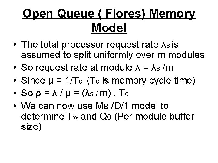
Open Queue ( Flores) Memory Model • The total processor request rate λs is assumed to split uniformly over m modules. • So request rate at module λ = λs /m • Since µ = 1/Tc (Tc is memory cycle time) • So ρ = λ / µ = (λs / m). Tc • We can now use MB /D/1 model to determine Tw and Q 0 (Per module buffer size)

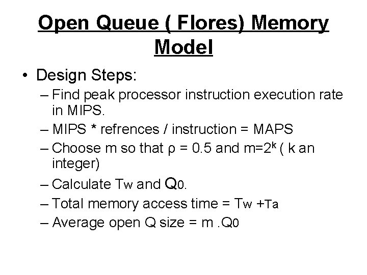
Open Queue ( Flores) Memory Model • Design Steps: – Find peak processor instruction execution rate in MIPS. – MIPS * refrences / instruction = MAPS – Choose m so that ρ = 0. 5 and m=2 k ( k an integer) – Calculate Tw and Q 0. – Total memory access time = Tw +Ta – Average open Q size = m. Q 0

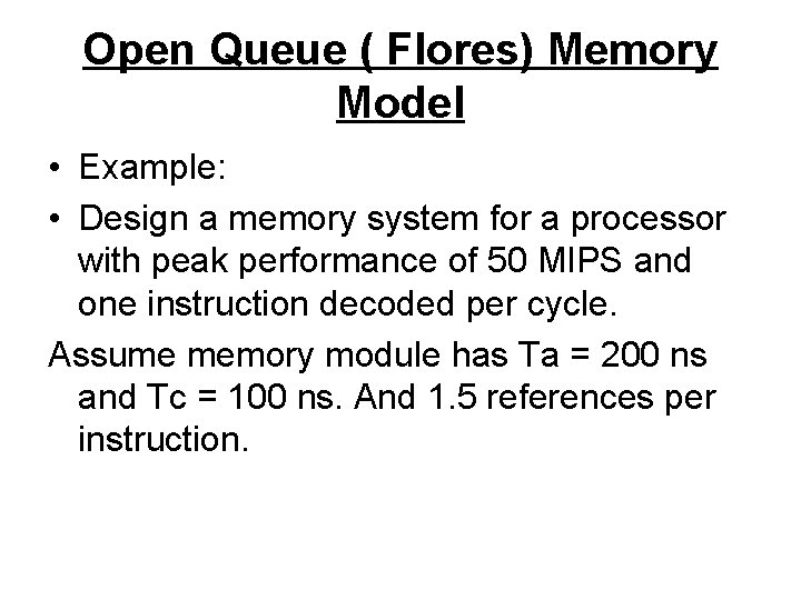
Open Queue ( Flores) Memory Model • Example: • Design a memory system for a processor with peak performance of 50 MIPS and one instruction decoded per cycle. Assume memory module has Ta = 200 ns and Tc = 100 ns. And 1. 5 references per instruction.

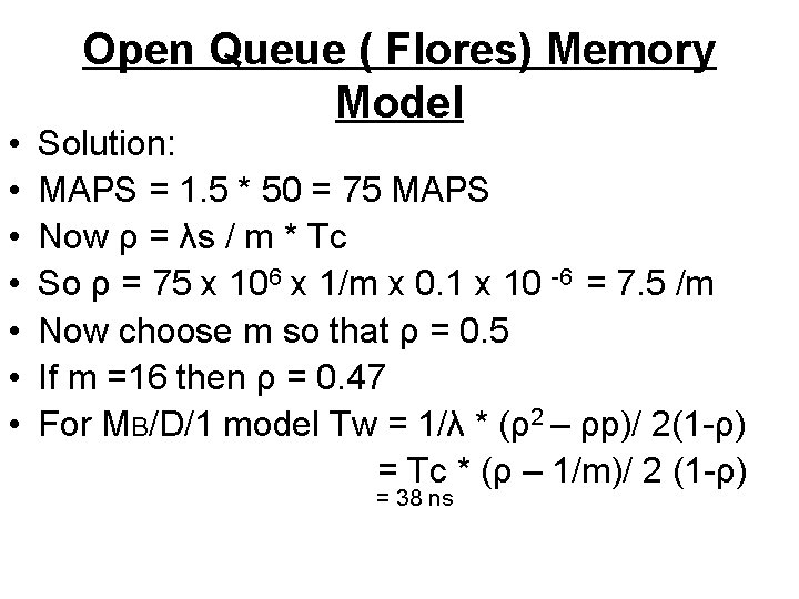
• • Open Queue ( Flores) Memory Model Solution: MAPS = 1. 5 * 50 = 75 MAPS Now ρ = λs / m * Tc So ρ = 75 x 106 x 1/m x 0. 1 x 10 -6 = 7. 5 /m Now choose m so that ρ = 0. 5 If m =16 then ρ = 0. 47 For MB/D/1 model Tw = 1/λ * (ρ2 – ρp)/ 2(1 -ρ) = Tc * (ρ – 1/m)/ 2 (1 -ρ) = 38 ns

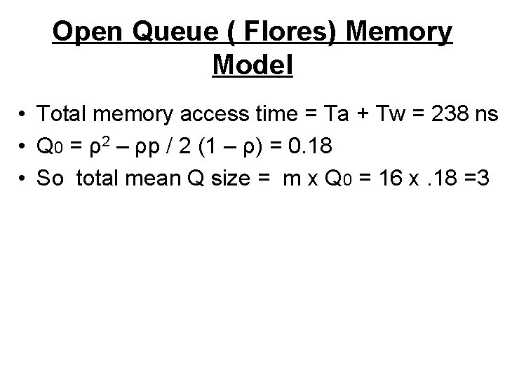
Open Queue ( Flores) Memory Model • Total memory access time = Ta + Tw = 238 ns • Q 0 = ρ2 – ρp / 2 (1 – ρ) = 0. 18 • So total mean Q size = m x Q 0 = 16 x. 18 =3

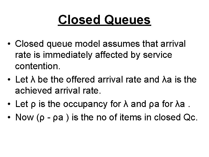
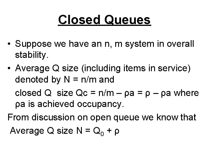
Closed Queues • Closed queue model assumes that arrival rate is immediately affected by service contention. • Let λ be the offered arrival rate and λa is the achieved arrival rate. • Let ρ is the occupancy for λ and ρa for λa. • Now (ρ - ρa ) is the no of items in closed Qc.

Closed Queues • Suppose we have an n, m system in overall stability. • Average Q size (including items in service) denoted by N = n/m and closed Q size Qc = n/m – ρa = ρ – ρa where ρa is achieved occupancy. From discussion on open queue we know that Average Q size N = Q 0 + ρ

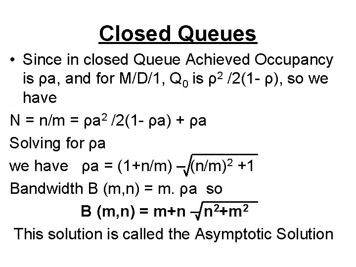
Closed Queues • Since in closed Queue Achieved Occupancy is ρa, and for M/D/1, Q 0 is ρ2 /2(1 - ρ), so we have N = n/m = ρa 2 /2(1 - ρa) + ρa Solving for ρa we have ρa = (1+n/m) – (n/m)2 +1 Bandwidth B (m, n) = m. ρa so B (m, n) = m+n – n 2+m 2 This solution is called the Asymptotic Solution

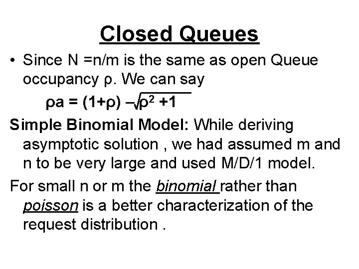
Closed Queues • Since N =n/m is the same as open Queue occupancy ρ. We can say ρa = (1+ρ) – ρ2 +1 Simple Binomial Model: While deriving asymptotic solution , we had assumed m and n to be very large and used M/D/1 model. For small n or m the binomial rather than poisson is a better characterization of the request distribution.

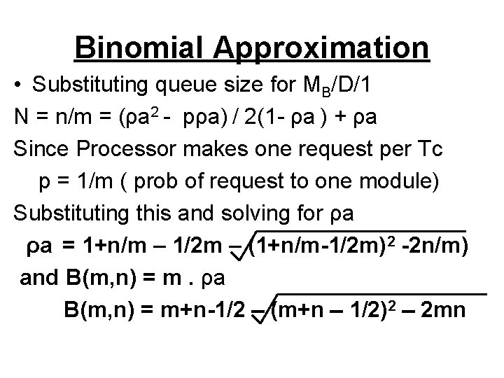
Binomial Approximation • Substituting queue size for MB/D/1 N = n/m = (ρa 2 - pρa) / 2(1 - ρa ) + ρa Since Processor makes one request per Tc p = 1/m ( prob of request to one module) Substituting this and solving for ρa ρa = 1+n/m – 1/2 m – (1+n/m-1/2 m)2 -2 n/m) and B(m, n) = m. ρa B(m, n) = m+n-1/2 - (m+n - 1/2)2 - 2 mn

Binomial Approximation • Binomial approximation is useful whenever we have – Simple processor memory configuration ( a binomial arrival distribution) – n >= 1 and m >= 1. – Request response behavior: where processor makes exactly n requests per Tc

The (δ) Binomial Model • If simple processor is replaced with a pipelined processor with buffer ( I-buffer, register set , cache etc) the simple binomial model may fail. • Simple binomial model can not distinguish between single simple processor making one request per Tc with probability =1, and two processors each making 0. 5 requests per Tc. • In second case there can be contention and both processors may make request with varying probability.

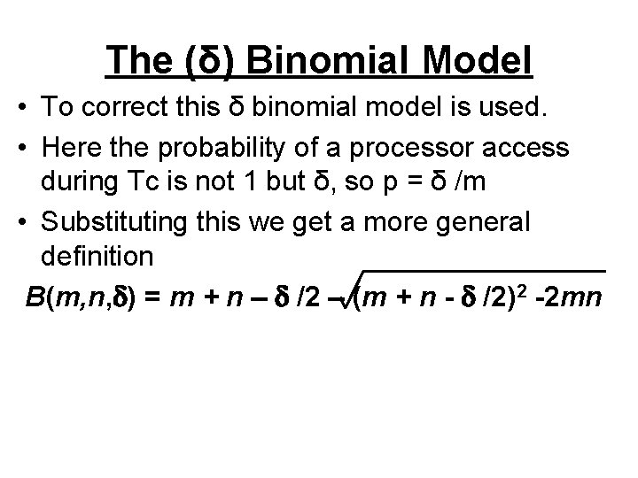
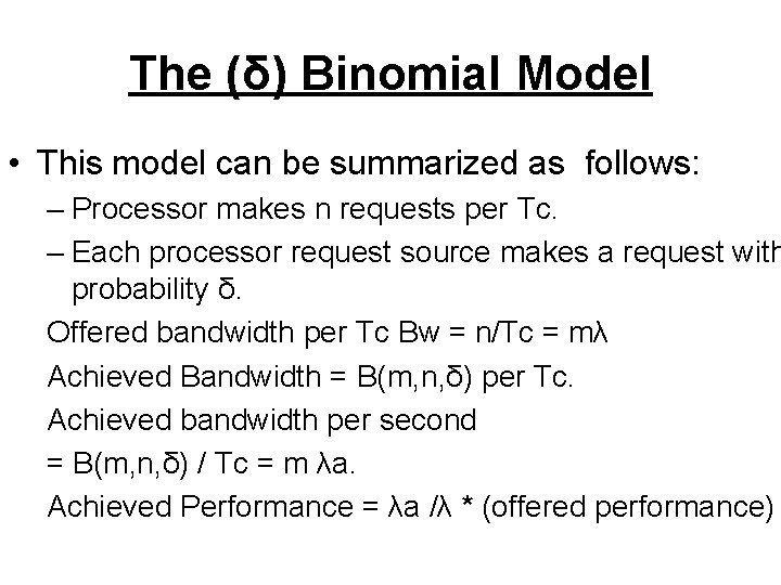
The (δ) Binomial Model • To correct this δ binomial model is used. • Here the probability of a processor access during Tc is not 1 but δ, so p = δ /m • Substituting this we get a more general definition B(m, n, ) = m + n - /2 - (m + n - /2)2 -2 mn

The (δ) Binomial Model • This model is useful in many processor designs where the source is buffered or makes requests on a statistical basis • If n is the mean request rate and z is the no. of sources, then = n/z

The (δ) Binomial Model • This model can be summarized as follows: – Processor makes n requests per Tc. – Each processor request source makes a request with probability δ. Offered bandwidth per Tc Bw = n/Tc = mλ Achieved Bandwidth = B(m, n, δ) per Tc. Achieved bandwidth per second = B(m, n, δ) / Tc = m λa. Achieved Performance = λa /λ * (offered performance)

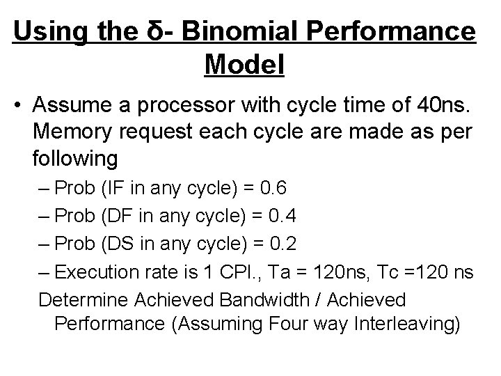
Using the δ- Binomial Performance Model • Assume a processor with cycle time of 40 ns. Memory request each cycle are made as per following – Prob (IF in any cycle) = 0. 6 – Prob (DF in any cycle) = 0. 4 – Prob (DS in any cycle) = 0. 2 – Execution rate is 1 CPI. , Ta = 120 ns, Tc =120 ns Determine Achieved Bandwidth / Achieved Performance (Assuming Four way Interleaving)

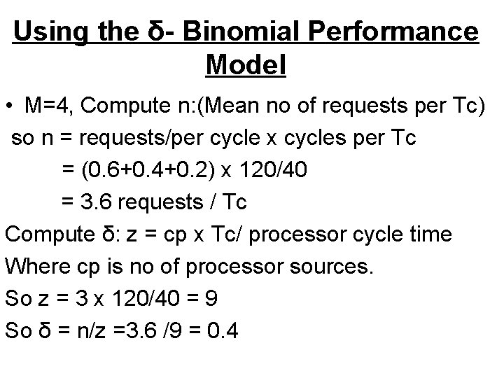
Using the δ- Binomial Performance Model • M=4, Compute n: (Mean no of requests per Tc) so n = requests/per cycle x cycles per Tc = (0. 6+0. 4+0. 2) x 120/40 = 3. 6 requests / Tc Compute δ: z = cp x Tc/ processor cycle time Where cp is no of processor sources. So z = 3 x 120/40 = 9 So δ = n/z =3. 6 /9 = 0. 4

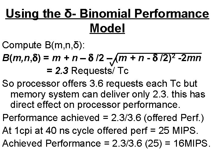
Using the δ- Binomial Performance Model Compute B(m, n, δ): B(m, n, ) = m + n - /2 - (m + n - /2)2 -2 mn = 2. 3 Requests/ Tc So processor offers 3. 6 requests each Tc but memory system can deliver only 2. 3. this has direct effect on processor performance. Performance achieved = 2. 3/3. 6 (offered Perf. ) At 1 cpi at 40 ns cycle offered perf = 25 MIPS. Achieved Performance = 2. 3/3. 6 (25) = 16 MIPS.

Comparison of Memory Models • Each model is valid for a particular type of processor memory interaction. • Hellerman’s model represents simplest type of processor. Since processor can not skip over conflicting requests and has no buffer, it achieves lowest bandwidth. • Strecker’s model anticipates out of order requests but no queues. Its applicable to multiple simple un buffered processors.

Comparison of Memory Models • M/D/1 open (Flores) Model has limited accuracy still it is useful for initial estimates or in mixed queue models. • Closed Queue MB/D/1 model represent a processor memory in equilibrium, where queue length including the item in service equals n/m on a per module basis. • Simple binomial model is suitable only for processors making n requests per Tc

Comparison of Memory Models • The δ binomial model is suitable for simple pipelined processors where n requests per Tc are each made with probability δ.

Review and Selection of Queuing Models • There are basically three dimensions to simple (single) server queuing models. • These three represent the statistical characterization of arrival Rate, Service rate and amount of buffering present before system saturates. • For arrival rate, if the source always requests service during a service interval, Use MB or simple binomial model.

Review and Selection of Queuing Models • If the particular requestor has diminishingly small probability of making a request during a particular service interval, use poisson arrival. • For service rate if service time is fixed , use constant (D) service distribution. • If service time varies but variance is unknown, (choose c 2=1 for ease of analysis) use exponential (M) service distribution.

Review and Selection of Queuing Models • If variance is known and C 2 can be calculated use M/G/1 model. • The third parameter determining the simple queuing model is amount of buffering available to the requestor to hold pending requests.

Processors with Cache • The addition of a cache to a memory system complicates the performance evaluation and design. • For CBWA caches, the requests to memory consists of line read and line write requests. • For WTNWA caches, its line read requests and word write requests. • In order to develop models of memory systems with caches two basic parameters must be evaluated

Processors with Cache 1. T line access , time it takes to access a line in memory. 2. Tbusy , potential contention time (when memory is busy and processor/cache is able to make requests to memory)

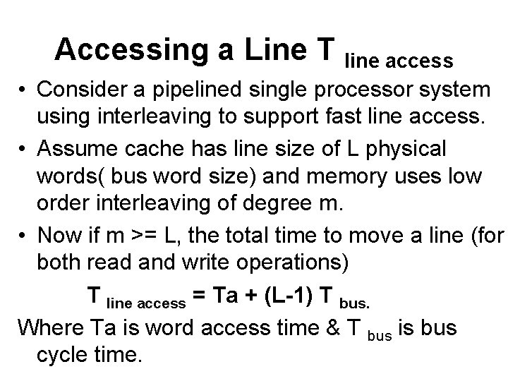
Accessing a Line T line access • Consider a pipelined single processor system using interleaving to support fast line access. • Assume cache has line size of L physical words( bus word size) and memory uses low order interleaving of degree m. • Now if m >= L, the total time to move a line (for both read and write operations) T line access = Ta + (L-1) T bus. Where Ta is word access time & T bus is bus cycle time.

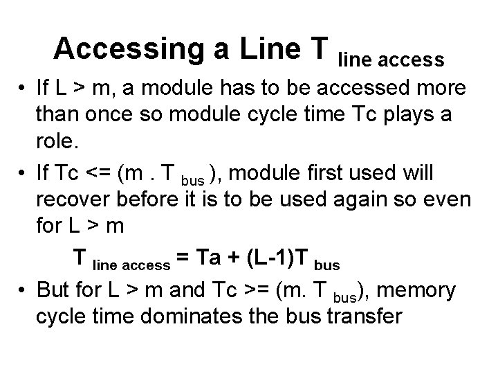
Accessing a Line T line access • If L > m, a module has to be accessed more than once so module cycle time Tc plays a role. • If Tc <= (m. T bus ), module first used will recover before it is to be used again so even for L > m T line access = Ta + (L-1)T bus • But for L > m and Tc >= (m. T bus), memory cycle time dominates the bus transfer

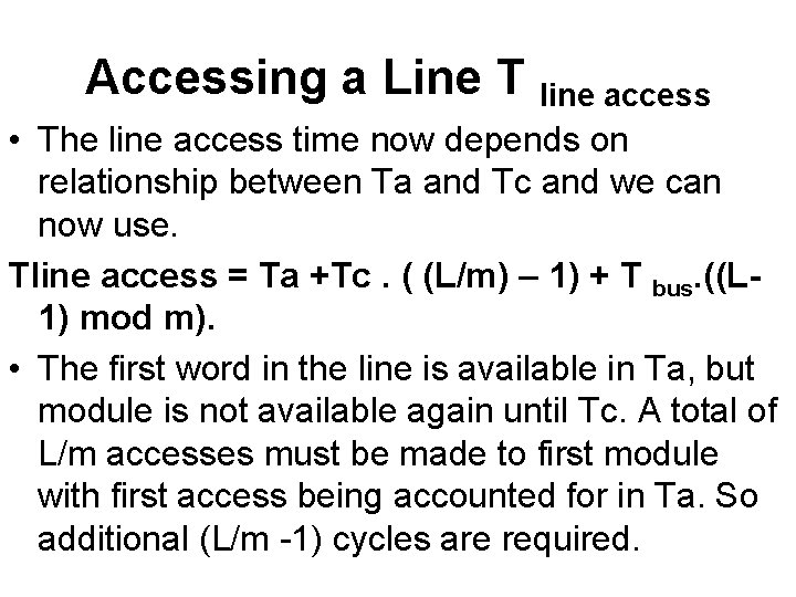
Accessing a Line T line access • The line access time now depends on relationship between Ta and Tc and we can now use. Tline access = Ta +Tc. ( (L/m) – 1) + T bus. ((L 1) mod m). • The first word in the line is available in Ta, but module is not available again until Tc. A total of L/m accesses must be made to first module with first access being accounted for in Ta. So additional (L/m -1) cycles are required.

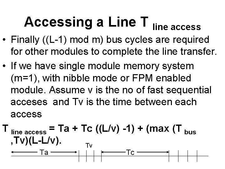
Accessing a Line T line access • Finally ((L-1) mod m) bus cycles are required for other modules to complete the line transfer. • If we have single module memory system (m=1), with nibble mode or FPM enabled module. Assume v is the no of fast sequential acceses and Tv is the time between each access T line access = Ta + Tc ((L/v) -1) + (max (T bus , Tv)(L-L/v). Tv Ta Tc

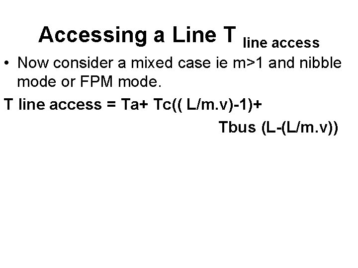
Accessing a Line T line access • Now consider a mixed case ie m>1 and nibble mode or FPM mode. T line access = Ta+ Tc(( L/m. v)-1)+ Tbus (L-(L/m. v))

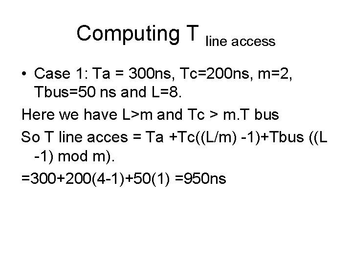
Computing T line access • Case 1: Ta = 300 ns, Tc=200 ns, m=2, Tbus=50 ns and L=8. Here we have L>m and Tc > m. T bus So T line acces = Ta +Tc((L/m) -1)+Tbus ((L -1) mod m). =300+200(4 -1)+50(1) =950 ns

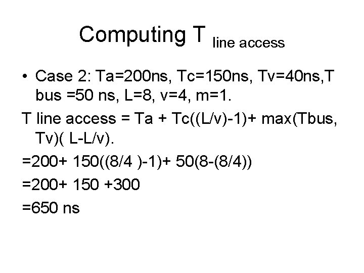
Computing T line access • Case 2: Ta=200 ns, Tc=150 ns, Tv=40 ns, T bus =50 ns, L=8, v=4, m=1. T line access = Ta + Tc((L/v)-1)+ max(Tbus, Tv)( L-L/v). =200+ 150((8/4 )-1)+ 50(8 -(8/4)) =200+ 150 +300 =650 ns

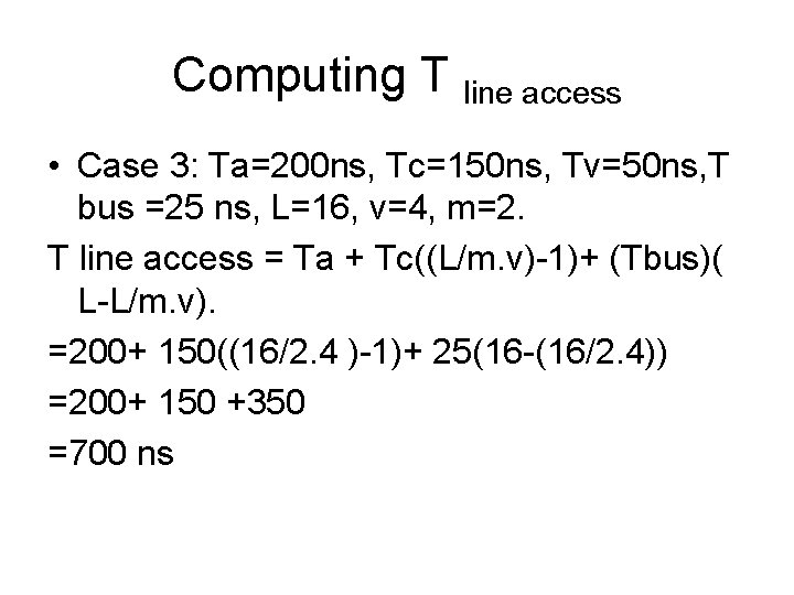
Computing T line access • Case 3: Ta=200 ns, Tc=150 ns, Tv=50 ns, T bus =25 ns, L=16, v=4, m=2. T line access = Ta + Tc((L/m. v)-1)+ (Tbus)( L-L/m. v). =200+ 150((16/2. 4 )-1)+ 25(16 -(16/2. 4)) =200+ 150 +350 =700 ns

Contention Time & Copy back Caches • In a simple copy back cache processor ceases on cache miss and does not resume until dirty line (w =probability of dirty line) is written back to main memory and new line read into the cache. The Miss time penalty thus is T miss =(1+w) T line access

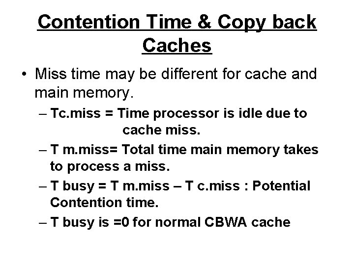
Contention Time & Copy back Caches • Miss time may be different for cache and main memory. – Tc. miss = Time processor is idle due to cache miss. – T m. miss= Total time main memory takes to process a miss. – T busy = T m. miss – T c. miss : Potential Contention time. – T busy is =0 for normal CBWA cache

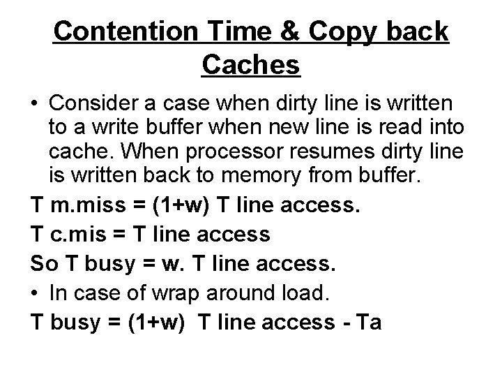
Contention Time & Copy back Caches • Consider a case when dirty line is written to a write buffer when new line is read into cache. When processor resumes dirty line is written back to memory from buffer. T m. miss = (1+w) T line access. T c. mis = T line access So T busy = w. T line access. • In case of wrap around load. T busy = (1+w) T line access - Ta

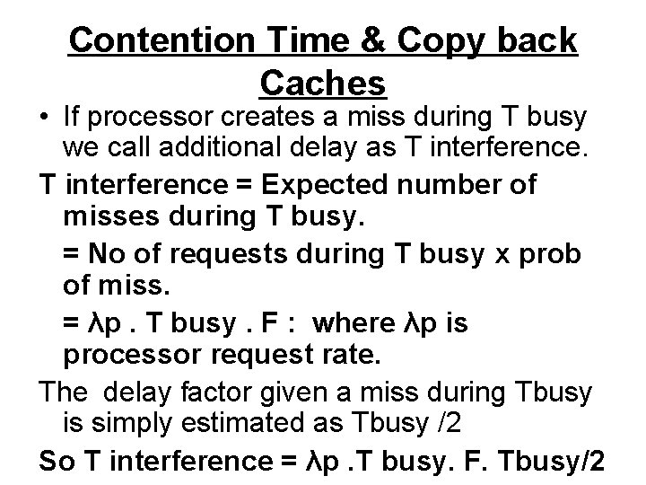
Contention Time & Copy back Caches • If processor creates a miss during T busy we call additional delay as T interference = Expected number of misses during T busy. = No of requests during T busy x prob of miss. = λp. T busy. F : where λp is processor request rate. The delay factor given a miss during Tbusy is simply estimated as Tbusy /2 So T interference = λp. T busy. F. Tbusy/2

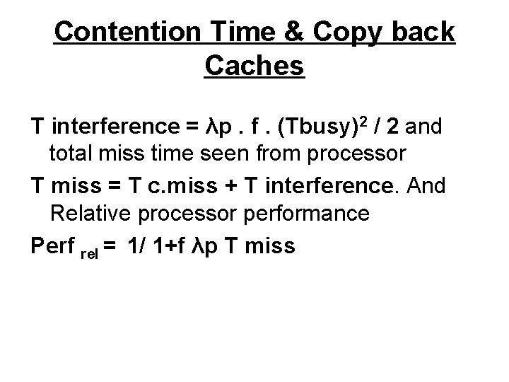
Contention Time & Copy back Caches T interference = λp. f. (Tbusy)2 / 2 and total miss time seen from processor T miss = T c. miss + T interference. And Relative processor performance Perf rel = 1/ 1+f λp T miss