Unit 4 Coating from Vapor Phase PVD CVD

 Introduction 1. Physical vapour deposition (PVD) is fundamentally a vaporisation coating")


 • The physical vapor deposition technique is based on the")
: thermal evaporation The number of molecules leaving a unit area")
 coil of refractory metal heater and a charge rod")
: thermal evaporation This is the relation between vapor pressure of")
: thermal evaporation From kinetic theory the mean free path relates")


 Weak substrate binding, q large; e. g. Au on")
 ln.")


: sputtering Momentum transfer -V working voltage - i discharge")
 Porous and/or amorphous -> results from poor surface mobility due")
, film cracking")

: MBE, Laser Ablation - • MBE (Molecular beam epitaxy) –")
: Ion cluster plating • • Ionized cluster: it is possible")
: Ion cluster plating and ion plating • • Gas cluster")


: reaction mechanisms • Mass transport of the reactant in the")


 Combustion Chemical Vapor Deposition")
: reaction mechanisms • Energy sources for deposition: • – Thermal")
 : reaction mechanisms • Mass flow controlled regime (square root")
 Silane: Si.")
 Si(s) + 2 H 2(g) Si.")
: step coverage • Step coverage, two factors are important –")
 : overview • CVD (thermal) – APCVD (atmospheric) – LPCVD")
 : L-CVD • The L-CVD method is able to fabricate")
 • Plasma-Enhanced CVD (PE-CVD) • Remote")
CVD As the flow of thermal energy gets more constrained while more")


 Si. O 2 LTO TEOS")


 + Arsine (As. H 3)=> Ga. As The various techniques of")
")
, also known")
 is a process used to deposit thin films")


- Slides: 78
Unit 4 – Coating from Vapor Phase PVD, CVD, Various Methods Used, Mechanism, Important Reactions Involved, and Applications Reference: Fabrication Engineering at the Micro and Nanoscale by Stephen A. Campbell
Physical Vapour Deposition(PVD) Introduction 1. Physical vapour deposition (PVD) is fundamentally a vaporisation coating technique, involving transfer of material on an atomic level. It is an alternative process to electroplating 2. The process is similar to chemical vapour deposition (CVD) except that the raw materials/precursors, i. e. the material that is going to be deposited starts out in solid form, whereas in CVD, the precursors are introduced to the reaction chamber in the gaseous state. Working Concept PVD processes are carried out under vacuum conditions. The process involved four steps: 1. Evaporation 2. Transportation 3. Reaction 4. Deposition
Evaporation During this stage, a target, consisting of the material to be deposited is bombarded by a high energy source such as a beam of electrons or ions. This dislodges atoms from the surface of the target, ‘vaporising’ them. Transport This process simply consists of the movement of ‘vaporised’ atoms from the target to the substrate to be coated and will generally be a straight line affair. Reaction In some cases coatings will consist of metal oxides, nitrides, carbides and other such materials. In these cases, the target will consist of the metal. The atoms of metal will then react with the appropriate gas during the transport stage. For the above examples, the reactive gases may be oxygen, nitrogen and methane. In instances where the coating consists of the target material alone, this step would not be part of the process.
Deposition This is the process of coating build up on the substrate surface. Depending on the actual process, some reactions between target materials and the reactive gases may also take place at the substrate surface simultaneously with the deposition process. The component that is to be coated is placed in a vacuum chamber. The coating material is evaporated by intense heat from, for example, a tungsten filament. An alternative method is to evaporate the coating material by a complex ion bombardment technique. The coating is then formed by atoms of the coating material being deposited onto the surface of the component being treated.
Variants of PVD include, in order of increasing novelty: Evaporative Deposition: In which the material to be deposited is heated to a high vapor pressure by electrically resistive heating in "high" vacuum. Electron Beam Physical Vapor Deposition: In which the material to be deposited is heated to a high vapor pressure by electron bombardment in "high" vacuum. Sputter Deposition: In which a glow plasma discharge (usually localized around the "target" by a magnet) bombards the material sputtering some away as a vapor. Cathodic Arc Deposition: In which a high power arc directed at the target material blasts away some into a vapor. Pulsed Laser Deposition: In which a high power laser ablates material from the target into a vapor.
Physical vapor deposition (PVD) • The physical vapor deposition technique is based on the formation of vapor of the material to be deposited as a thin film. The material in solid form is either heated until evaporation (thermal evaporation) or sputtered by ions (sputtering). In the last case, ions are generated by a plasma discharge usually within an inert gas (argon). It is also possible to bombard the sample with an ion beam from an external ion source. This allows to vary the energy and intensity of ions reaching the target surface.
Physical vapor deposition (PVD): thermal evaporation The number of molecules leaving a unit area of evaporant per second 6
Resistive evaporation source using (a) coil of refractory metal heater and a charge rod and (b) Standard thermal source including a dimpled boar in a resistive media Electron beam evaporative sources (a) low flux source using a hot wire electron and a thin movable rod and (b) 270 o source arc in which beam can raster across the surface of charge by a magnet • PVD uses mainly physical processes to produce reactant species in the gas phase and to deposit films • In evaporation, source material is heated in high vacuum chamber (P<10 -5 torr) • Mostly line of sight deposition since pressure is low • Deposition rate is determined by emitted flux and by geometry of the target and wafer holder
Physical vapor deposition (PVD): thermal evaporation This is the relation between vapor pressure of the evaporant and the evaporation rate. If a high vacuum is established, most molecules/atoms will reach the substrate without intervening collisions. Atoms and molecules flow through the orifice in a single straight track, or we have free molecular flow : The fraction of particles scattered by collisions with atoms of residual gas is proportional to: The source-to-wafer distance must be smaler (e. g, 25 to 70 cm)
Physical vapor deposition (PVD): thermal evaporation From kinetic theory the mean free path relates to the total pressure as: Since thickness of the deposited film, t, is proportional to the cos b, the ratio of the film thickness shown in the figure on the right with = 0° is given as:
Evaporation Step Coverage The step coverage of evaporated films is poor due to the directional nature of the evaporated material (shadowing) (see figure 12 -5). Heating (resulting in surface diffusion) and rotating the substrates (minimizing the shadowing) help with the step coverage problem, but evaporation can not form continuous films for aspect ratios (AR=step height/step width or diameter) greater than 1. We need a less directional metalization scheme====> Higher pressures!
Thin Film Growth Modes
Homogeneous Nucleation • Spontaneous nucleation in gas phase • no surface, dust, charge, etc. • undesirable in practice -> polycrystals • If solid has vapor pressure P∞ & pressure of vapor above solid is P • If P= P∞, vapor does not condensate, solid does not evaporate • If P> P∞, vapor condenses • PV = NRT = nk. T (where N=number of moles, R=gas constant, n=number of molecules, k=Boltzman constant) • When vapor condenses, Energy change, DGv =Gibbs free energy of formation and is negative As atoms add to the nucleus, it grows with the release of free energy and solid-vapor interface grows resulting in increase in free energy s/unit area Total increase in energy: DGhomo = (4/3)pr 3 DGv+4 pr 2 s; Max. at r* = -2 s/DGv; DG*=(16 p/3) (s 3/DGv 2) For nucleus r<r*, DG decrease by breaking up For nucleus r>r*, DG decreases by growth If P/P∞ is large, i. e. high supersaturation, DGv increases and r* decreases Note: As r* -> ratomic, values of s, surface concept can not be used
Heterogeneous Nucleation • Introduce substrate, dust etc. in vapor • Consider adatoms on substrate, Nad/unit area re-evaporation probability: W=n exp (Qad/k. T) Where Qad=binding energy to substrate (negative) deposition N↓ re-evaporation N↑ Nad Substrate Re-evaporation rate: N↑=Nad n exp (Qad/k. T) At steady state: N↑=N↓ -> Nad=(N↓/n) exp (-Qad/k. T) Residence time, t=W-1=n-1 exp(Qdes/k. T); where, Qdes= desorption energy (positive) Adsorption rate: Assuming only adatom population with no further interaction • If N↓ 0(deposition stopped), Nad 0 (all eventually re-evaporated) • Adsorption rate: d. Nad/dt = N↓ - N↑ = N↓ - Nad/t d. Nad/ (N↓t - Nad)= dt/t On integrating, Nad(t) = N↓t(1 -exp-t/t) ; For Nad=0 at t=0 For t<<t, Nad(t) =N↓t (i. e. independent of time for weak physical adsorption) For t>>t, Nad(t) =N↓t (i. e. complete condensation for strong adsorption or initial transient)
Heterogeneous Nucleation: Surface Diffusion Surface diffusion of adatoms by distance X from point of impact X=(2 Dt)1/2 = (2 D)1/2 n-1/2 exp(-Qad/2 k. T); Where, D=surface diffusivity = a 2 nexp(Qdiff/k. T) X=21/2 aexp-((Qdiff +Qad)/2 k. T); Where, a=interatomic distance • When adjacent nuclei separation < X; no further nuclei created -> all atoms join existing nuclei • Capillary Model For island clusters with ІQadІ >> k. T (cold substrate/metal on metal) N ↑small & Nad large, interatomic collisions > clustering DG=a 3 r 3 DGv+a 1 r 2 s. V-C+a 2 r 2 s. S-C-a 2 r 2 s. S-V Where DG = Free energy of condensation (negative)=(k. T/V)ln(N↓/N↑); V=molecular volume) On differentiating; DG/ r = 3 a 3 r 2 DGv+2 a 1 rs. V-C+2 a 2 r(s. S-C-s. S-V) and equating to 0 at r* = critical radius; DG* = [4(a 1 s. V-C+a 2 s. S-C-a 2 s. S-V)]/(27 a 32 DGv 2) = [4 p(s. V-C 3)3 DGv 2](2+cos )(1 -cos )2 For spherical cap nucleus r*=[-2(a 1 s. V-C+a 2 s. S-C-a 2 s. S-V)]/3 a 3 DGv = -2 s. V-C/DGv
Spherical Cap: General Trend a) Weak substrate binding, q large; e. g. Au on glass b) High supersaturation ratio (N↓/N↑ small r* (e. g. low vapor pressure material) (e. g. W), cold substrate, high deposition rate, strong substrate adhesion; Continuity reached early (many small islands) c) DGv large, r* 0, No nucleation barrier, monolayer formation (or ss-v high So, sc-v +sc-s ~ ss-v) d) r*/ T)N↓ > 0; r*/ N↓)T <0 but large DN↓ required for significant Dr* • Charging effects on nucleation: No initial barrier to nucleation; only barrier to growth • Field enhances coalescence, field can inhibit nucleation or enhance nucleation • Surface defects increase DG* and r* but less atoms/critical nucleus Nucleation Rate Adatom residence time, t = n-1 exp(Qdes/k. T); where, Qdes= desorption energy (positive) Nucleation rate NR = N*A*w; where N*=exp(-DG*/k. T); ns=nucleation site density, A*=2 pr*aosin ; w=t. N↓D; NR = 2 pr*aosin PNA/(2 p. MRT)1/2 nsexp(Edes-Ediff-DG*)/k. T (Rate of creation super critical nucleus
Nucleation Rate-Contd. Note: NR a exp-DG*/k. T DG* a DGV-2 DGV a ln(N↓/N↑) ln. NR a [ln(N↓/N↑)]2 (N↓/N↑) = super saturation ratio
Sputter Deposition A plasma at higher pressure is used to “knock” metal atoms out of a target. These energetic atoms deposit on a wafer located near the target. The higher pressure produces better step coverage due to more random angled delivery. The excess energy of the ions also aids in increasing the surface mobility • Uses plasma to sputter target, dislodge atoms and deposit on wafers to form film. • Higher pressures than evaporation (1 -100 torr) • Better at depositing alloys and compounds than evaporation • Plasma contains Ar positive ions, electrons, and neutral Ar atoms Threshold energy: Where Advantages: Better step coverage, less radiation damage than E-beam evaporation, easier to deposit allots Disadvantages: Some plasma damage including implanted Ar, Good for ohmics but not Schottky diodes
DC Sputter Deposition - Working Principle • Most of voltage drop of the system (due to applied DC voltage, Vc) occurs over cathode sheath • Ar+ ions are accelerated across cathode to the negatively cathode, striking the electrode and sputtering off atoms. These atoms travel through plasma and deposit on wafers sitting on anode. • Rate of sputtering depends on the sputtering yield, Y, defined as number of atoms or molecules ejected from the target per incident ion • Y is a function of energy and mass of ions, and the target material. It is also a function of incident angle.
Isotropic flux arrival Non-Isotropic flux arrival • Sputtering targets are generally large and provide a wide range of arrival angles in contrast to a point source • Arrival angle distribution generally described by a cosn (i. e. normal component of flux striking the surface determines the deposition or growth rate • Size and type of source, system geometry and collisions in gas phase play an important in distribution of arrival angle.
Factors Affecting Sputtering Yield vs. Target Yield vs. angle of incidence Yield vs. Ion energy
Effect of Substrate Bias • Substrate biasing reduces the yield (i. e. lower deposition rate) • Substrate biasing helps in good adhesion with the substrate during initial stage of deposition; subsequently biasing voltage is switched off. • Sputter surface cleaning also helps to improve adhesion of coating with the substrate.
Cylindrical and Planar Magnetron T: Target, P: plasma; SM: solenoid; M: magnet; E: electric field; B: magnetic field
The main difference is that the power used in RF sputtering is AC, while that in DC sputtering is DC. Basically, during DC sputtering, the working gas will be ionized. As a result, many positive ions will be produced within the chamber and accumulate on the surface of target If the conductivity of target you sputtering is not very good.
The use of DC in a plasma requires electrically conductive electrodes. If one or both of the electrodes are non-conductive, e. g. when the glow discharge is used for the deposition of dielectric films, where the electrodes become gradually covered with insulating material, the insulator would charge up and terminate the discharge.
The use of an alternative current AC power source can alleviate this problem because positive charges accumulated during one half-cycle can be neutralized by electron bombardment during the next cycle. The frequencies generally used for these alternating voltages are typically in the radiofrequency (RF) range (1 k. Hz– 103 MHz; with a most common value of 13. 56 MHz
RF Sputter Deposition • For DC sputtering, target electrode is conducting • To sputter dielectric materials use RF power source • Due to slower mobility of ions vs. , electrons, the plasma biases positively with respect to both electrodes (DC current = 0); Therefore, continuous sputtering. • When electrodes areas are not equal, field must be higher at the smaller electrode (higher current density) to maintain overall current continuity • Thus by making the target electrode smaller, sputtering occurs “only” on the target. Wafer electrode can also be connected to chamber walls, further increasing V 2/V 1
Sputtering Contamination
Physical vapor deposition (PVD): sputtering Momentum transfer -V working voltage - i discharge current - d, anode-cathode distance - PT, gas pressure - k proportionality constant
Sputtered Film Characteristics 1) Porous and/or amorphous -> results from poor surface mobility due to low temperature, low ion energy (Low RF power/DC bias or higher pressures, less acceleration 2) T (transition)-Zone: small grain polycrystalline, dense, smooth, and high reflectance results from higher surface mobility due to higher temperature or ion energy 3) Further increases in surface mobility results in columnar grains that have rough surfaces and poor coverage 4) Still further increase in surface mobility result in large (non-columnar) grains. These grains can be good for diffusion barriers (less grain boundary diffusion due to fewer grains) but pose problems for lithography due to light scatter off of large grains and tend to be more rigid leading to more failures in electrical lines.
Film Stresses Film stress can result in wafer bowing (problem with lithography), film cracking or peeling. 1) Extrinsic stress (force acting on the wafer due to sources external to the deposited film) Thermal induced stress Y: Young’s modulus, a: thermal expansion coefficient, n: Poisson’s ratio 2. Intrinsic Stress (forces acting on the wafer due to sources internal to the deposited film) such as differences in atomic spacing, variation in grain orientation or size, grain growth during depositing and implanted trapped gaseous impurities such as Ar. Ø Both these stresses can lead to a bowed wafer with deflection d given by: Where, D=wafer thickness, t=film thickness, R=radius of the wafer bow
Evaporation and Sputtering: Comparison Evaporation Sputtering Rate 1000 atomic layers/sec (e. g. 0. 5 mm/min. for Al) 1 atomic layer/sec Choice of materials Limited Almost unlimited Purity Better (no gas inclusions, very high vacuum) Possibility of incorporating impurities (low medium vacuum range) Substrate heating Very low Unless magnetron is used substrate heating is substantial Surface damage Very low, with e-beam x Ionic bombardment damage -ray damage is possible In-situ cleaning Not an option Easily done with sputter etch Alloy compositions, stochiometry Little or no control Alloy composition can be tightly controlled X-ray damage Only with e-beam evaporation Radiation and particle damage is possible Changes in source material Easy Expensive
Physical vapor deposition (PVD): MBE, Laser Ablation - • MBE (Molecular beam epitaxy) – Epitaxy: homo-epitaxy (1 material) hetero-epitaxy (2 or more materials) – Very slow: 1µm/hr – Very low pressure: 10 -11 Torr • Laser sputter deposition – Complex compounds (e. g. HTSC (high temp. super conductor, biocompatible ceramics)
Physical vapor deposition (PVD): Ion cluster plating • • Ionized cluster: it is possible to ionize atom clusters that are being evaporated leading to a higher energy and a film with better properties (adherence, density, etc. ). – From 100 mbar (heater cell) to 10 -5 to 10 -7 mbar (vacuum)-sudden cooling – Deposits nanoparticles Combines evaporation with a plasma • faster than sputtering • complex compositions • good adhesion
Physical vapor deposition (PVD): Ion cluster plating and ion plating • • Gas cluster ions consist of many atoms or molecules weakly bound to each other and sharing a common electrical charge. As in the case of monomer ions, beams of cluster ions can propagate under vacuum and the energies of the ions can be controlled using acceleration voltages. A cluster ion has much larger mass and momentum with lower energy per atom than a monomer ion carrying the same total energy. Upon impact on solid surfaces, cluster ions depart all their energy to an extremely shallow region of the surface. Cluster plating material is forced sideways and produces highly smooth surfaces. Also individual atoms can be ionized and lead to ion plating (see figure on the right, example coating : very hard Ti. N)
Alloy Deposition
Summary of Merits and Demerits of evaporation methods Method E-Beam Evaporation Filament Evaporation Sputter Deposition Merits Demerits 1. high temp materials 1. some CMOS processes sensitive to 2. good for liftoff radiation 3. highest purity 2. alloys difficult 3. poor step coverage 1. simple to implement 2. good for liftoff 1. limited source material (no high temp) 2. alloys difficult 3. poor step coverage 1. better step coverage 1. possible grainy films 2. alloys 2. porous films 3. high temp 3. plasma damage/contamination materials 4. less radiation damage
Importance of PVD Coatings • PVD coatings are deposited for numerous reasons. Some of the main ones are: • Improved hardness and wear resistance • Reduced friction • Improved oxidation resistance • The use of such coatings is aimed at improving efficiency through improved performance and longer component life. • They may also allow coated components to operate in environments that the uncoated component would not otherwise have been able to perform.
Advantages • Materials can be deposited with improved properties compared to the substrate material • Coating temperature is below the final heat treating temperature • Small, precisely reproducible coating thickness • High wear resistance • Low frictional coefficient • Almost any type of inorganic material can be used as well as some kinds of organic materials • The process is more environmentally friendly than processes such as electroplating Disadvantages • It is a line of sight technique meaning that it is extremely difficult to coat undercuts and similar surface features • High capital cost • Some processes operate at high vacuums and temperatures requiring skilled operators • Processes requiring large amounts of heat require appropriate cooling systems • The rate of coating deposition is usually quite slow
Applications PVD coatings are generally used to improve hardness, wear resistance and oxidation resistance. Thus, such coatings use in a wide range of applications such as: Aerospace Automotive Surgical/Medical Dies and moulds for all manner of material processing Cutting tools Fire arms 4040
Summary of Key Ideas • Thin film deposition is a key technology in modern IC fabrication. • Topography coverage issues and filling issues are very important, especially as geometries continue to decrease. • CVD and PVD are the two principal deposition techniques. • In PVD systems arrival angle distribution is very important in determining surface coverage. Shadowing can be very important. • A wide variety of systems are used in manufacturing for depositing specific thin films, e. g. magnetron sputtering. • Advanced simulation tools are becoming available, which are very useful in predicting topographic issues. • Generally these simulators are based on physical models of mass transport and surface reactions and utilize parameters like arrival angle and sticking coefficients from direct and indirect fluxes to model local deposition rates. • Thin film stress can be due to differential CTEs, impurities, and grain growth.
CVD-Overview • What is CVD? • Types of CVD – MO-CVD, PE-CVD, etc • CVD process / applications
What is CVD Process? • Chemical Vapor Deposition is the formation of a nonvolatile solid film on a substrate by the reaction of vapor phase chemicals (reactants) that contain the required constituents. • The reactant gases are introduced into a reaction chamber and are decomposed and reacted at a heated surface to form the thin film.
CVD Process Applications • Microfabrication processes widely use CVD to deposit materials in various forms, including: monocrystalline, polycrystalline, amorphous, and epitaxial. These materials include: silicon, carbon fiber, carbon nanofibers, filaments, carbon nanotubes, Si. O 2, silicon-germanium, tungsten, silicon carbide, silicon nitride, silicon oxynitride, titanium nitride, and various high-k dielectrics. The CVD process is also used to produce synthetic diamonds.
Chemical vapor deposition (CVD): reaction mechanisms • Mass transport of the reactant in the bulk • Gas-phase reactions (homogeneous) • Mass transport to the surface • Adsorption on the surface • Surface reactions (heterogeneous) • Surface migration • Incorporation of film constituents, island formation • Desorption of by-products • Mass transport of by-produccts in bulk CVD: Diffusive-convective transport of depositing species to a substrate with many intermolecular collisionsdriven by a concentration gradient Si. H 4 4 Si
Family of CVD Technologies
Chemical Vapor Deposition • • CVD => Chemical Vapor Deposition PE-CVD => Plasma Enhanced CVD MO-CVD => Metal Organic CVD Atmospheric pressure CVD (AP-CVD) Low-pressure CVD (LP-CVD) Ultrahigh vacuum CVD (UHV-CVD) Aerosol assisted CVD (AA-CVD) Direct liquid injection CVD (DLICVD)
Other Types of Chemical Vapor Deposition Atomic layer CVD (ALCVD) Combustion Chemical Vapor Deposition (CCVD) Hot wire CVD (HWCVD) Hybrid Physical-Chemical Vapor Deposition (HPCVD) • Rapid thermal CVD (RTCVD) • Vapor phase epitaxy (VPE) • •
Chemical vapor deposition (CVD): reaction mechanisms • Energy sources for deposition: • – Thermal – Plasma – Laser – Photons Deposition rate or film growth rate Laminar flow (U) d(x) (Fick’s first law) L (Boundary layer thickness) (gas viscosity h, gas density r, gas stream velocity U) (Dimensionless Reynolds number) (by substitution in Fick’s first law and Dx=d) dx
Chemical vapor deposition (CVD) : reaction mechanisms • Mass flow controlled regime (square root of gas velocity)(e. g. AP CVD~ 100 -10 k. Pa) : FASTER • Thermally activated regime: rate limiting step is surface reaction (e. g. LP CVD ~ 100 Pa---D is very large) : SLOWER
Basic CVD Concept Example: Si deposition by CVD (assume atmospheric pressure (APCVD) Silane: Si. H 4(g) ↔ Si. H 2(g) + 2 H(g); Reaction constant: Si. H 2(g) ↔ Si. H 2(a); Si. H 2(a) ↔ Si(s) + H 2(g) (a: adsorbed; s: solid) Where f’s: flow rates A simple prototype thermal CVD reactor
CVD Reactions Pyrolysis: Thermal decomposition Si. H 4(g) Si(s) + 2 H 2(g) Si. H 2 Cl 2(g) Si(s) + 2 HCl(g) CH 4(g) C(diamond/graphite)+2 H 2(g) Ni(CO)4(g) Ni(s) + 4 CO(g) Oxidation: Si. H 4(g) + 2 O 2(g) Si. O 2(s) + 2 H 2 O(g) 3 Si. H 4(g) + 4 NH 3(g) Si 3 N 4(s) + 12 H 2(g) Hydrolysis: 2 Al. Cl 3(g) + 3 H 2 O(g) Al 2 O 3(s) + 6 HCl(g) Reduction: WF 6(g) + 3 H 2(g) W(s) + 6 HF(g) Displacement: Ga(CH 3)3(g) + As. H 3(g) Ga. As(s) + 3 CH 4(g) Zn. Cl 2(g) + H 2 S(g) Zn. S(s) + 2 HCl(g) 2 Ti. Cl 4(g) + 2 NH 3(g) + H 2(g) Ti. N(s) + 8 HCl(g)
Chemical vapor deposition (CVD): step coverage • Step coverage, two factors are important – Mean free path and surface migration i. e. P and T – Mean free path: l = q=1800 z is angle of arrival q=900 a w q=2700
Chemical vapor deposition (CVD) : overview • CVD (thermal) – APCVD (atmospheric) – LPCVD (<10 Pa) – VLPCVD (<1. 3 Pa) • PE CVD (plasma enhanced) • Photon-assisted CVD • Laser-assisted CVD • MOCVD
Chemical vapor deposition (CVD) : L-CVD • The L-CVD method is able to fabricate continuous thin rods and fibres by pulling the substrate away from the stationary laser focus at the linear growth speed of the material while keeping the laser focus on the rod tip, as shown in the Figure. LCVD was first demonstrated for carbon and silicon rods. However, fibers were grown from other substrates including silicon, carbon, boron, oxides, nitrides, carbides, borides, and metals such as aluminium. The L-CVD process can operate at low and high chamber pressures. The growth rate is normally less than 100 µm/s at low chamber pressure (<<1 bar). At high chamber pressure (>1 bar), high growth rate (>1. 1 mm/s) has been achieved for smalldiameter (< 20 µm) amorphous boron fibers.
Plasma Enhanced CVD • Microwave plasma-assisted CVD (MP-CVD) • Plasma-Enhanced CVD (PE-CVD) • Remote plasma-enhanced CVD (RPE-CVD)
Plasma Enhanced (PE)CVD As the flow of thermal energy gets more constrained while more layers are added for multi-layer metallization, we want to come down with the temperature for the oxide ( or other) CVD processes. One way for doing this is to supply the necessary energy for the chemical reaction by ionizing the gas, thus forming a plasma.
Applications of CVD
CVD Reactors Horizontal APCVD Reactor
Thermal CVD Reactor Chemical Vapor Deposition Apparatus
Chemical Vapor Deposition
CVD Growth Model
Comparison CVD Process Advantages Disadvantages Applications APCVD Simple, Fast Deposition, Low Temperature Poor Step Coverage, Contamination Low-temperature Oxides LPCVD Excellent Purity, Excellent Uniformity, Good Step Coverage, Large Wafer Capacity High Temperature, Slow Deposition High-temperature Oxides, Silicon Nitride, Poly. Si, W, WSi 2 Chemical and Particle Contamination Low-temperature Insulators over Metals, Nitride Passivation PECVD Low Temperature, Good Step Coverage
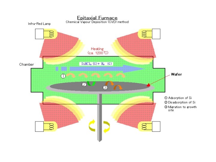
Silicon CVD ‘Epitaxy’ • When Si. H 4 gas is used in a CVD reactor, a Si layer is deposited on the wafer surface. The size of the crystallites depends on the deposition temperature. • At high enough temperature, the ad-atoms have enough kinetic energy to move on the surface and align themselves with the underlying Si. • This is an epitaxial layer, and the process is called Epitaxy instead of CVD. • At lower deposition temperatures, the layer is poly -crystalline Si (consisting of small crystallites)
Silicon Epitaxy Process The chemical reaction that produces the Si is fairly simple: Si. Cl 4(g)+2 H 2(g)=(1000 -1200 o. C)=Si(s)+4 HCl(g) Instead of Si. Cl 4 you may want to use Si. HXCl 4 -X
CVD Used in Semiconductors Layer Reaction equations Temperature (ºC) Si. O 2 LTO TEOS HTO Si. H 4 + O 2 -> Si. O 2 + 2 H 2 Si(OC 2 H 5)4 -> Si. O 2 + gas. RP Si. Cl 2 H 2 + N 2 O -> Si. O 2 + 2 N 2 + 2 HCl Si. H 4 + CO 2+H 2 -> Si. O 2 + gas. RP 400 -450 650 -700 850 -950 Si 3 N 4 3 Si. H 2 Cl 2 + 4 NH 3 -> Si 3 N 4 + 6 HCl + 6 H 2 700 -900 Si. H 4 -> Si + 2 H 2 600 -650 Polysilicon Tungsten selective 2 WF 6 + 3 Si -> 2 W + 3 Si. F 4 blanket WF 6 + Si. H 4 -> W + Si. F 4 + 2 HF + H 2 300 400 -450
Silicon Oxide CVD Process There are several possibilities, one is Si. H 2 CI 2 + 2 NO 2 = (900 °C) = Si. O 2 + 2 HCI + 2 N 2 While this reaction was used until about 1985, a better reaction is offered by the "TEOS" process. Si(C 2 H 5 O)4 = (720 °C) = Si. O 2 + 2 H 2 O + C 2 H 4. Si(C 2 H 5 O)4 has the chemical name Tetraethylorthosilicate
MO-CVD • A technique for growing thin layers of compound semiconductors in which metal organic compounds, having the formula MRx, where M is a group III metal and R is an organic radical, are decomposed near the surface of a heated substrate wafer, in the presence of a hydride of a group V element. Abbreviated MOCVD.
MO-CVD: Trimethylgallium (TMG) + Arsine (As. H 3)=> Ga. As The various techniques of growing epitaxial layers from the vapor phase can be divided roughly into two categories depending on whether the species are transported physically or chemically from the source to the substrate. In the physical transport techniques (Physical Vapor Deposition - PVD), the compound to be grown or its constituents are evaporated and subsequently transported through the relevant reactor toward the substrate. In the chemical transport techniques (Chemical Vapor Deposition - CVD), volatile species containing the constituent elements of the layer to be grown are produced first in- or outside the reactor and transported as streams of vapor towards the reaction zone near the substrate. These gaseous species subsequently undergo chemical reactions or dissociate thermally to form the reactants which participate in the growth of the film. The practical demand to decrease the growth temperature generated an intensive development trend of CVD processes based on metal organic compounds, decomposing at lower temperatures. This process is referred to as Metal Organic Chemical Vapor Deposition (MOCVD) or Organometallic Vapor Phase Epitaxy. The classical example is the growth of Ga. As from Trimethylgallium (TMG) and Arsine (As. H 3). In our laboratory we apply this technique to grow Ga. N from TMG and Ammonia. However, this technique is based on a very precise control of the gas flow as can be estimated from the look into the gas mixing cabinet.
Planetary MOCVD reactor in an industrial setup (Photo courtesy of Aixtron)
Metal Organic Vapor Phase Epitaxy MO-VPE Metal organic vapor phase epitaxy (MOVPE), also known as organometallic vapor phase epitaxy (OMVPE) or metal organic chemical vapor deposition (MOCVD), is a chemical vapour deposition method of epitaxial growth of materials, especially compound semiconductors, from the surface reaction of organic compounds or metalorganics and metal hydrides containing the required chemical elements. For example, indium phosphide could be grown in a reactor on a substrate by introducing Trimethylindium ((CH 3)3 In) and phosphine (PH 3). Formation of the epitaxial layer occurs by final pyrolysis of the constituent chemicals at the substrate surface. In contrast to molecular beam epitaxy (MBE) the growth of crystals is by chemical reaction and not physical deposition.
PE-CVD Plasma-enhanced chemical vapor deposition (PECVD) is a process used to deposit thin films from a gas state (vapor) to a solid state on a substrate. Chemical reactions are involved in the process, which occur after creation of a plasma of the reacting gases. The plasma is generally created by RF (AC) frequency or DC discharge between two electrodes, the space between which is filled with the reacting gases
PE-CVD Apparatus Thermal - chemical vapor deposition A thermal-CVD system was built for carbon nanotubes production via gas phase or on substrate surface. The sketch of thermal-CVD system consists of quartz tube furnace which can operate till 1200 degree centigrade. The sketch of our equipment is shown in figure 1. Main advantages of a thermal-CVD are: the absolute ability for mass production of nanotubes material and the controllable growth of carbon nanotubes at a specific location on a substrate for incorporation in electronic device. Plasma Enhanced - chemical vapor deposition A controllable method for carbon nanotubes production is plasma enhanced-CVD. Such a system is often used to grow free standing vertically aligned MWCNT. The set-up which our laboratory is equipped with is a glow discharged type. Briefly, two electrodes are placed in a stainless-steel chamber. The grounded cathode plays the role of a substrate holder and Ohmic heater. On the anode is applied aprox. 400 V. Advantages: • Significantly lower process temp. are possible than for CVD • Precise coatings Disadvantages: • Only limited suitability for bore holes, slots etc.
Low Pressure RF Plasma for PECVD of Ti. O 2 on Plastics
CVD Coatings and their properties. CVD Coatings containing On to various substrates Properties Chromium Solid solution alloys (i) with Iron, Nickel and Cobalt (ii) on Iron as carbides and nitrides (i) Corrosion / oxidation resistance (ii) Wear / corrosion resistance Aluminium As Aluminides with Iron, Cobalt and Nickel High temperature oxidation resistance Boron As Borides with Iron, Cobalt and Nickel Wear / erosion resistance Silicon As Silicides with Iron, Tungsten and Molybdenum High temperature oxidation resistance Titanium As Carbides, nitrides and carbonitride on ferrous and non-ferrous alloys Wear resistance Manganese Solid solution alloys on carbon steels Wear resistance
Advantages of CVD Can be used for a wide range of metals and ceramics Can be used for coatings or freestanding structures Fabricates net or near-net complex shapes Is self-cleaning—extremely high purity deposits (>99. 995% purity) Conforms homogeneously to contours of substrate surface Has near-theoretical as-deposited density Has controllable thickness and morphology Forms alloys Infiltrates fiber preforms and foam structures Coats internal passages with high length-to-diameter ratios Can simultaneously coat multiple components Coats powders
Applications CVD processes are used on a surprisingly wide range of industrial components, from aircraft and land gas turbine blades, timing chain pins for the automotive industry, radiant grills for gas cookers and items of chemical plant, to resist various attacks by carbon, oxygen and sulphur. Some important applications are listed below. Surface modification to prevent or promote adhesion Photoresist adhesion for semiconductor wafers Silane/substrate adhesion for microarrays (DNA, gene, protein, antibody, tissue) MEMS coating to reduce stiction (static friction) Bio. MEMS and biosensor coating to reduce "drift" in device performance Promote biocompatibility between natural and synthetic materials Copper capping Anti-corrosive coating