Unit 2 Field Effect Transistors Objectives BJT vs

Unit 2 Field Effect Transistors

Objectives: • • BJT v/s FET JFET MOSFET JFET v/s MOSFET Handling and biasing MOSFETs FET applications CMOS IGBT

5. 1 BJT v/s FET: 1. 2. 3. 4. 5. 6. Current controlled – voltage controlled Bipolar devices – unipolar devices Zi < 1 MΩ - Zi very high (100 s MΩ) Less temp. stable – more temp. stable Small size – smaller size More gain – less gain
: Intro. : • JFET simpler device among family •")
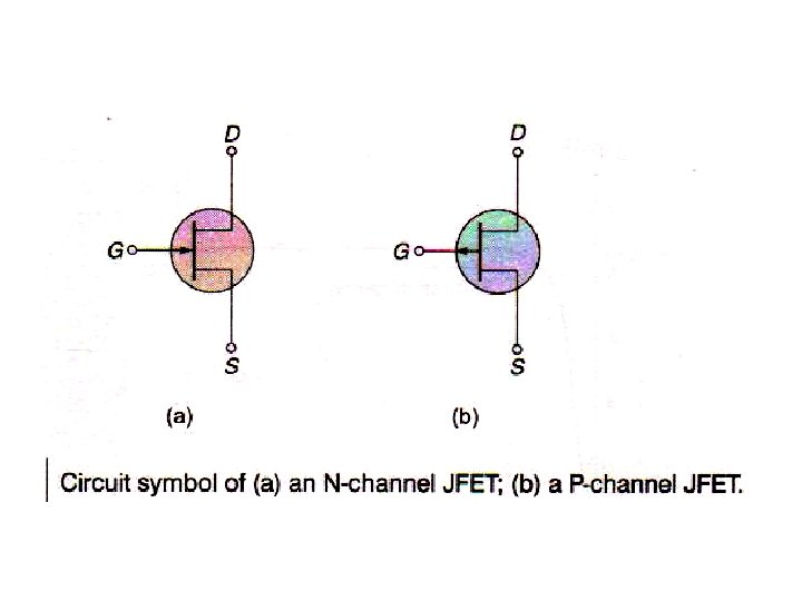
5. 2 JFET (junction FET): Intro. : • JFET simpler device among family • 3 – terminal device; 1 controls current through 2 • Types – – p - channel – n - channel

Construction

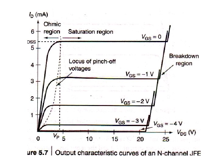
Characteristic:

Characteristic:

Transfer characteristics:
 in saturation region is given by: r. D")
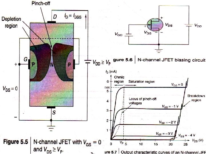
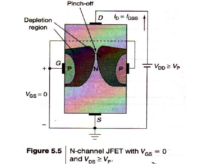
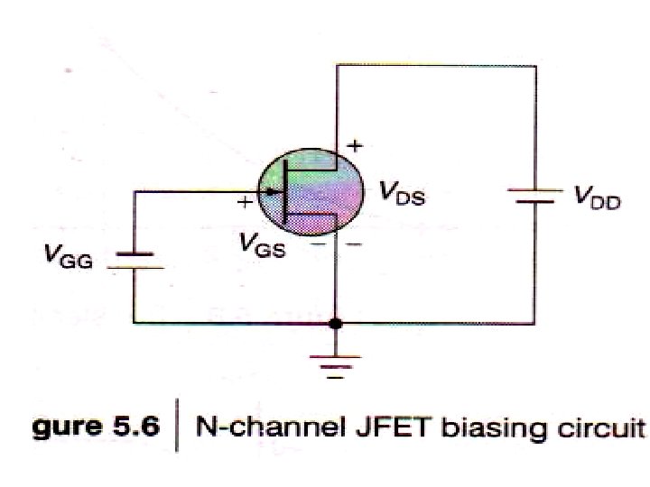
• The drain resistance (rd) in saturation region is given by: r. D rd = ----------(1 -VGS / VP)2 Where rd is drain resistance at VGS = 0 & r. D is drain resistance at particular VGS

• Relationship between output drain current & input gate-to-source voltage: ID = IDSS VGS 1 - ------VP 2

Effect of temperature: • • • Better thermal stability ? JFET temperature ↑ Depletion region width ↓ & Increase channel width ↑ ID ↑ Thus in above steps: • T ↑ ID ↑ • Positive temperature coefficient • Carrier mobility ↓ • ID ↓ Thus in above steps: • T ↑ ID ↓ • Negative temperature coefficient
: What exactly metal oxide? -MOSFET is insulated from")
5. 3 Metal oxide FET (MOSFET): What exactly metal oxide? -MOSFET is insulated from the semiconductor channel by very thin oxide (Si. O 2) layer • These are also known as insulated gate (IG) FET • MOSFET types / modes: – Depletion MOSFET (De-MOSFET) – Enhancement MOSFET (E-MOSFET)

DE-MOSFET: • There is no ptype gate • There is no direct electrical connection between gate & channel • Capacitive effect exists between gate & channel

Symbols:

Circuit connection: Do not copy

Characteristics: Enhancement mode / region, +ve charge carriers from p-substrate contribute Depletion mode / region, Normal operation as MOSFET

Transfer characteristics:

E-MOSFET: • ha Notice that the channel is not fabricated, It will be generated

Symbols:

Working: • Capacitive effect induces electrons from psubstrate • Creating a n-channel

Characteristics:

E-MOSFET Transfer characteristics:

Differences between JFET & MOSFET: 1. Operational modes: 1. JFET -depletion mode 2. DE-MOSFET -depletion / enhancement modes 3. E-MOSFET-enhancement mode 2. MOSFET – input resistance high compared to JFET 3. JFETs have higher drain resistance rd than MOSFETs 4. Leakage current in MOSFET is less compared to JFET 5. MOSFETs are easier to construct & widely used than JFETs

Handling MOSFETs: • • Si. O 2 layer is thin & prone to damage Due to static charges, potential difference between Si. O 2 can result in breakdown & establish conduction through it Precautions: 1. Person handling ground himself properly 2. Connect zener diodes, back-to-back as shown
")
Biasing MOSFETs: Biasing DE-MOSFETs: • Same as JFETs • Example: Fixed bias (page 183)

Biasing E-MOSFETs: Feedback biasing configuration:

KVL at input VDD –IG RG - ID RD - VGS = 0 VGS = VDD – ID RD -----(1) KVL at output VDS = VDD – ID RD -----(2)

Voltage divider bias: Assignment #1: Numerical examples 5. 9 & 5. 10 on pages 196 & 197

FET applications: 1. 2. 3. 4. 5. 6. Amplifier Analog switch Multiplexer Current limiter Voltage variable resistors Oscillators

Analog switch:

Multiplexer:

5. 13 CMOS devices: CMOS Inverter Operation: Vin=0 Q 2 ON & Q 1 OFF Vout=1 Vin=1 Q 1 ON & Q 2 OFF Vout=0
: • Have positive attributes of BJT & MOSFET • Faster")
Insulated Gate Bipolar (IGBT): • Have positive attributes of BJT & MOSFET • Faster switching like MOSFET • Lower ON – state voltage like BJT Application / Usage area: • SMPS • Motor control – as high voltage handling capacity • Induction heating control

Questions: 1. Explain JFET construction, biasing and characteristics, transfer characteristics 2. How better stability is achieved in JFET? 3. Explain DE-MOSFET (construction diagram, symbol, output & transfer characteristics, working) 4. Explain E-MOSFET ( --”--) 5. Difference between JFET & MOSFET 6. Explain biasing methods of De- & EMOSFETs

7. Example 5. 8, page 193 8. Example 5. 9, page 196 9. Explain Applications of FET 10. Explain CMOS inverter -----o 0 o-----
- Slides: 40