Unit 2 BASIC CIRCUIT CONCEPT SHEET RESISTANCE RS

Unit – 2 BASIC CIRCUIT CONCEPT

SHEET RESISTANCE RS •

Typical sheet resistance of MOS layer

Rs applied to MOS transistors & inverters

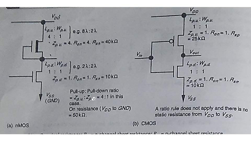
Cont… • n-type pass transistor has channel length & width =2 λ • Length to width ratio Z is 1: 1. for another L=8 λ & w=2 λ • Z=L/W=4 • Rs= ZRs =4 x 10⁴ ohm

Silicides • As line width becomes smaller Rs contributed to RC delay increases with polysilicon. • Scaling could be offset by interconnect resistance. • Silicides (2 -4 ohm) formed by depositing metal on polysilicon and then do sintering process. • Ways to deposit the metal • Sputtering or evaporation • Co-sputtering metal and silicon • Co-evaporation from the element.

Area capacitance of layer • Conduction Layer are separated from substrate and each other by insulator, thus llel plate capacitive effect is present. •

Standard unit of capacitance • Standard unit for a technology node is the gate - channel capacitance of the minimum sized transistor (2λ x 2λ), given as �Cg • This is a ‘technology specific’ value or standard value • For 5μm mos • Area = 5μm x 5μm = 25μm • Cap. Value = 4 x 10 -4 p. F/ μm 2 • �Cg = 4 x 10 -4 p. F/ μm 2 x 25μm =. 01 p. F

Area capacitance calculation • Ratio b/w area of interest and area of standard gate size (2 λx 2 λ) • Consider area in metal • Cap to substrate = • Consider area in polysilicon • Cap to substrate = Consider area in n-type diff. & Cap to substrate =

Area cap. For more then one layer • Consider the metal area

• Consider area in polysilicon • For transistor • Gate capacitance cg= 1�Cg • Total capacitance

Inverter delay • Consider basic 4: 1 Zp. u to Zp. d ratio nmos inverter • Consider cascaded inverter pair, delay will be constant irrespective to logic level transaction & assume τ = 0. 3 ns

Fig. min. size CMOS inverter • In cascaded cmos the gate capacitance is double bcz i/p is connected to both tr. gate

Formal estimation of CMOS inverter delay Rise –time estimation: sat current for pmos Current charges CL Vout = Idspt/CL Sub Idsp

Cont… • Assume t= τr and vout=+vdd • = 0. 2 vdd Fall time estimation

Rise time and fall time factor • To achieve symmetrical operation using min. channel length Wp=2. 5 Wn The input capacitance is 1�Cg + 2. 5 �Cg= 3. 5 �Cg Factor which affect rise time and fall time

DRIVING LARGE CAPACITIVE LOAD
 CASCADED INVERTERS AS DRIVERS")
i) CASCADED INVERTERS AS DRIVERS

Super buffer • Use super buffer to reduce delay problems • Vin =1 : Q 1, Q 2 & Q 4 Turned ON , Q 3 pull down to 0 with small delay • Vin =0: gate of Q 3 rise to Vdd, Q 4 is off & Q 3 made to conduct with Vdd • That is twice the avg. voltage would applied if gate tied to source.

• With 5μm tech – driving load of 2 p. F with 5 ns rise time

Bi. CMOS drivers • Tr having gm & I/A char. That are greatly superior to MOS – high I driving capabilities • I increases exponentially in BJT (with low Vbe) • Effect of temp. • Vbe depend on WB, NA, μn & Ic it is linearly depend on T • Tin – initial time to charge B to E junction(2 ns for Bi. Cmos, 1 ns for MOS & 50 -100 ps for Ga. As)

• TL- charge o/p load cap. Time is less for BJT by factor of hfe • Delay of bicmos INV. is

Cont. . • Delay related to Rc, high Rc lead to long propagation delay. • Buried subcollector region keeps Rc as low as possible.

Propagation delay Cascaded pass transistors: • delay introduced when the logic signals have to pass through a chain of pass transistors

• The transistors could pose a RC product delay Ex: the response at node V 2 is given by • C d. V 2/dt =(I 1 -I 2)= [(V 1 -V 2)-(V 2 -V 3)]/R • the distance along the network from the input (x). • The propagation time τp from a signal to propagate a distance x is τ p α X 2 • if all sheet resistance, gate-to-channel capacitance RS and □cg are lumped together Rtotal= nr Rs Ctotal= nc □Cg • overall delay for n sections τp = n 2 rc(τ)

Design of long polysilicon wires • Long polysilicon wires contribute distributed series R and C and inconsequence signal propagation is slowed down

Cont… • For long polysilicon runs, use buffers Effects : • signal propagation is speeded up • reduction in sensitivity to noise • input voltage spends a relatively long time in the vicinity of Vinv so that small disturbances.
Fringing fields • For fine line metallization, the value of fringing field")
Wiring capacitances (i)Fringing fields • For fine line metallization, the value of fringing field capacitance (Cff) can be of the order of area capacitance. • • • l = wire length t = thickness of wire d = wire to substrate separation. Then, total wire capacitance Cw= Carea+ Cff
 Interlayer capacitances • capacitance between the layers due to parallel plate effects. •")
ii) Interlayer capacitances • capacitance between the layers due to parallel plate effects. • knowing these capacitances--the accuracy of circuit modeling and delay calculations will be improved. iii)peripheral capacitance • p-diffusion regions & n-diffusion regions forms junctions with n-well & p-well resp. • diffusion regions (form diode structure) • Cp increases with reduction in source or drain area. (p. F/unit length) • Total diffusion capacitance is Cdiff= Carea+ Cp

• Choice of layers R C Low Low Moderate High

• Vdd and Vss lines must be distributed on metal lines due to low Rs value • Long lengths of poly must be avoided because they have large Rs • The resistance of the transistors are much larger, so there is no problem due voltage divider effects b/w wiring and transistor resistances • Diffusion areas must be carefully handled because they have larger capacitance to substrate. Avoid charge sharing.
- Slides: 32