Unit 06 PLDs Programmable Logic DevicePLDs Till now
Unit -06 PLDs
Programmable Logic Device(PLDs) • Till now we used MSI chips for designing different logic ckts. Due to their fixed functions, they are called as Fixed Function Ics. • There are two more approaches to design digital ckts. 1. ASICs (Application Specific Integrated Ckt) 2. PLDs (Programmable Logic Devices)
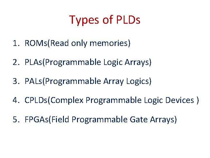
Types of PLDs 1. ROMs(Read only memories) 2. PLAs(Programmable Logic Arrays) 3. PALs(Programmable Array Logics) 4. CPLDs(Complex Programmable Logic Devices ) 5. FPGAs(Field Programmable Gate Arrays)
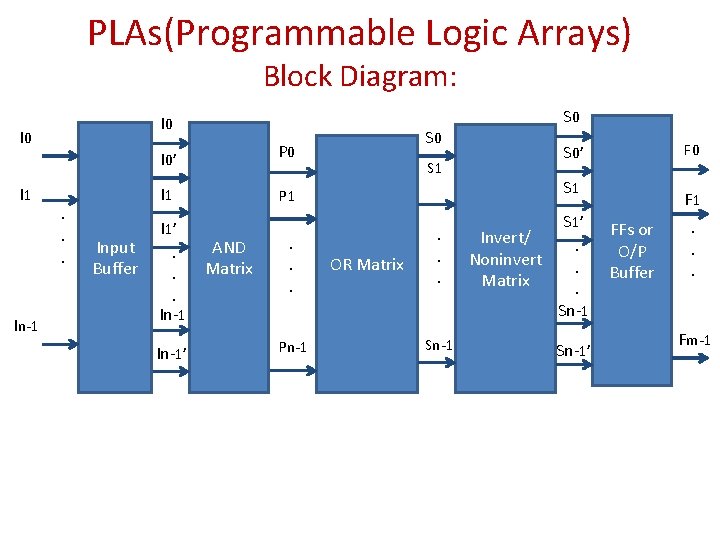
PLAs(Programmable Logic Arrays) Block Diagram: I 0 I 1 In-1 . . . Input Buffer I 0’ P 0 I 1 P 1 I 1’. . . In-1’ AND Matrix . . . Pn-1 S 0 S 1 OR Matrix . . . Sn-1 S 0 F 0 S 0’ S 1’ Invert/. Noninvert. Matrix. Sn-1’ F 1 FFs or O/P Buffer . . . Fm-1
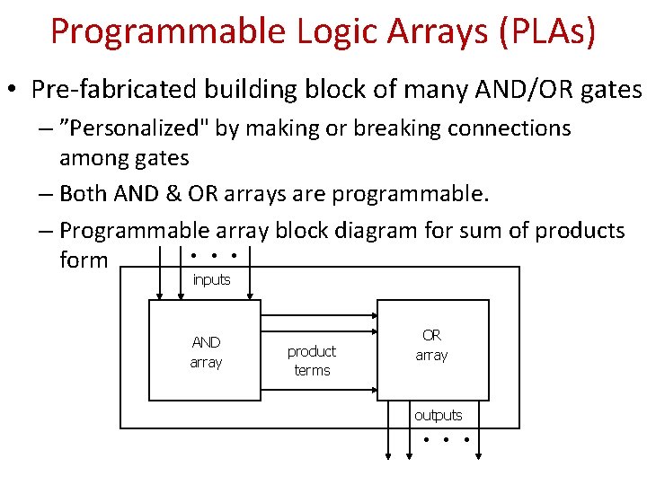
Programmable Logic Arrays (PLAs) • Pre-fabricated building block of many AND/OR gates – ”Personalized" by making or breaking connections among gates – Both AND & OR arrays are programmable. – Programmable array block diagram for sum of products • • • form inputs AND array product terms OR array outputs • • •
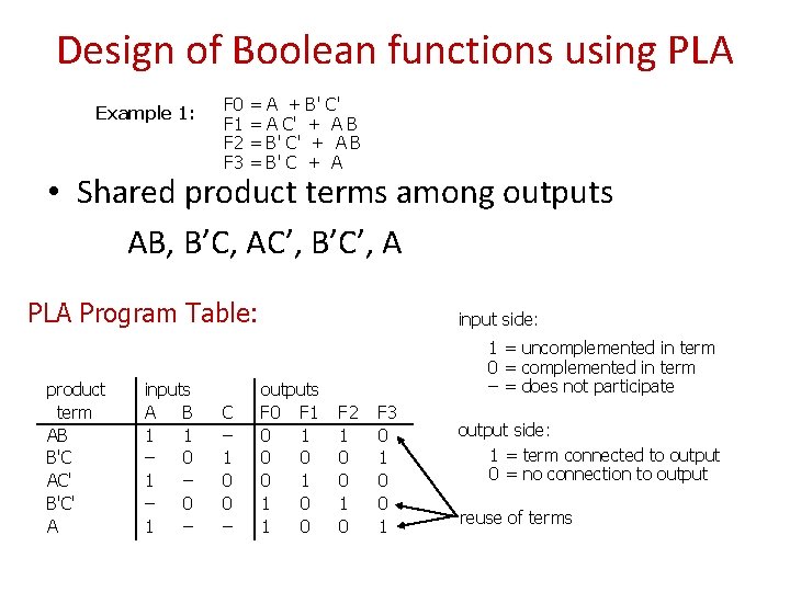
Design of Boolean functions using PLA Example 1: F 0 F 1 F 2 F 3 = = A + A C' B' C' + AB + A • Shared product terms among outputs AB, B’C, AC’, B’C’, A PLA Program Table: product term AB B'C AC' B'C' A inputs A B 1 1 – 0 1 – C – 1 0 0 – input side: outputs F 0 F 1 0 0 0 1 1 0 1 = uncomplemented in term 0 = complemented in term – = does not participate F 2 1 0 0 1 0 F 3 0 1 0 0 1 output side: 1 = term connected to output 0 = no connection to output reuse of terms
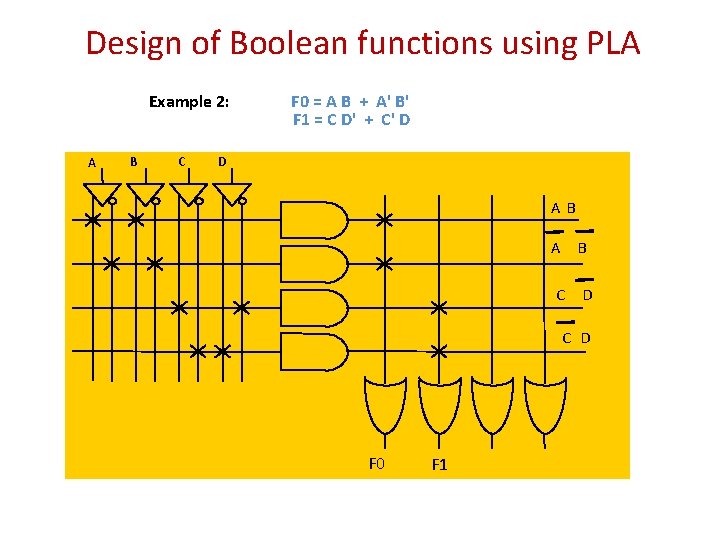
Design of Boolean functions using PLA Example 2: A B C F 0 = A B + A' B' F 1 = C D' + C' D D A B C D F 0 F 1
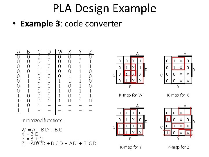
PLA Design Example • Example 3: code converter A 0 0 0 0 1 1 B 0 0 1 1 0 0 0 1 C 0 0 1 1 0 0 1 – D 0 1 0 1 0 1 – – W 0 0 0 1 1 1 – – X 0 0 1 1 0 0 – – Y 0 0 1 1 1 0 0 – – Z 0 1 1 0 – – minimized functions: W=A+BD+BC X = B C' Y=B+C Z = A'B'C'D + B C D + A D' + B' C D' A A 0 0 X 1 0 1 X 1 C 0 0 1 X X D 0 1 X 0 C 0 0 0 X X B B K-map for W K-map for X A D A 0 1 X 0 C 1 1 1 X X D 0 0 X 1 1 0 X 0 C 0 1 1 X X 0 X X B B K-map for Y K-map for Z D
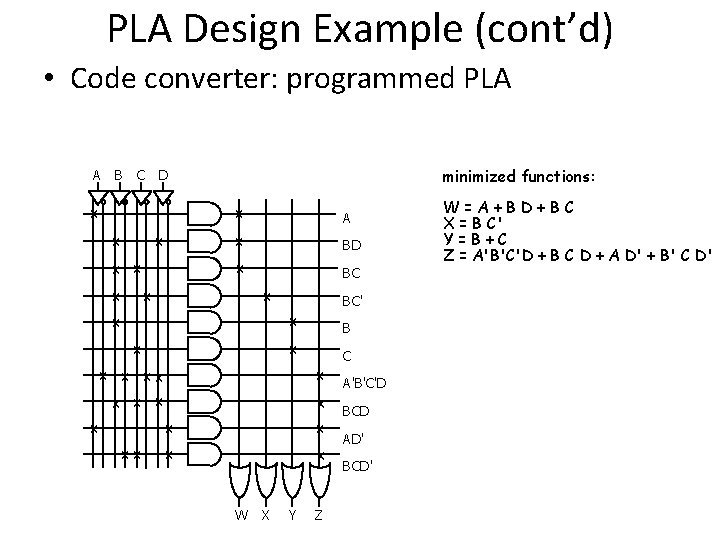
PLA Design Example (cont’d) • Code converter: programmed PLA A B minimized functions: C D x x x xx x x xx A BD BC x BC' x B x C x x x W X Y Z A'B'C'D BCD AD' BCD' W=A+BD+BC X = B C' Y=B+C Z = A'B'C'D + B C D + A D' + B' C D'
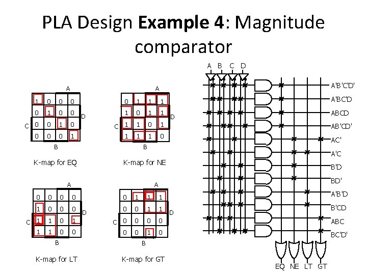
PLA Design Example 4: Magnitude comparator A B A C D A'B'C'D' A 1 0 0 C 0 0 0 1 D 0 1 1 C 1 1 1 0 B B K-map for EQ K-map for NE A A'BC'D ABCD D AB'CD' AC' A'C B'D BD' A 0 0 1 0 0 0 C 1 1 1 0 0 D 0 1 1 1 0 0 1 1 C 0 0 0 1 0 B B K-map for LT K-map for GT A'B'D B'CD D ABC BC'D' EQ NE LT GT
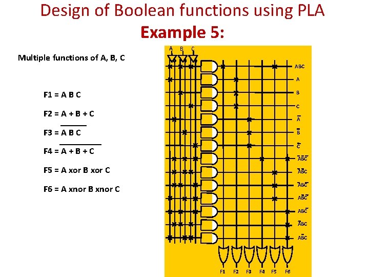
Design of Boolean functions using PLA Example 5: A Multiple functions of A, B, C B C ABC A F 1 = A B C F 2 = A + B + C A F 3 = A B C B F 4 = A + B + C C ABC F 5 = A xor B xor C ABC F 6 = A xnor B xnor C ABC ABC F 1 F 2 F 3 F 4 F 5 F 6
PALs(Programmable Array Logics) • Only AND array is Programmable • OR array is fixed. • Not as flexible as PLA.
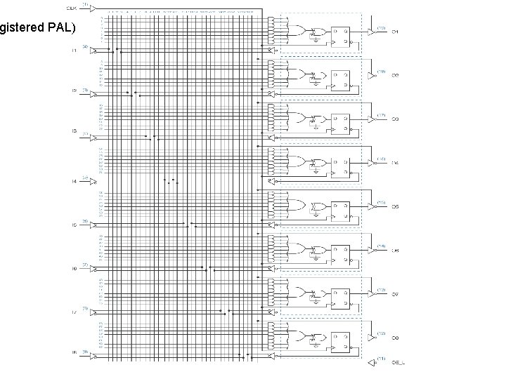
gistered PAL) 13
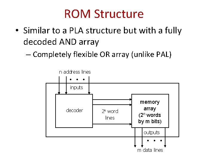
ROM Structure • Similar to a PLA structure but with a fully decoded AND array – Completely flexible OR array (unlike PAL) n address lines • • • inputs decoder 2 n word lines memory array (2 n words by m bits) outputs • • • m data lines
- Slides: 14