UNESCO Laboratory of Environmental Electrochemistry Charles University in


UNESCO Laboratory of Environmental Electrochemistry Charles University in Prague Heyrovský Institute AS CR

BORON DOPED DIAMOND FILM ELECTRODES - AN EXCELENT TOOL FOR VOLTAMMETRIC MONITORING OF ENVIRONMENTALLY IMPORTANT ORGANIC SUBSTANCES Jiri Barek UNESCO Laboratory of Environmental Electrochemistry, Department of Analytical Chemistry, Charles University, Prague, Czech Republic, e-mail: Barek@natur. cuni. cz

Why new electrode materials • • • Broader potential window Lower noise and background current Resistance toward passivation Mechanical stability Compatibility with „green analytical chemistry“

WHY BORON DOPED DIAMOND FILM ELECTRODES • • • Low noise Broad potential windows Low passivation Mechanical and electrochemical stability Biocompatibility Comercial availability

Boron doped diamond film electrodes Properties of diamond üsp 3 allotropic modification of carbon üHardness üLow chemical reactivity üInsulant doping by boron Properties of boron doped diamond üLow double layer capacity üBroad potential window üLow adsorption üStability, biocompatibility

BDDFE

The potential window of BDD electrode, BR buffer p. H 2 - 12

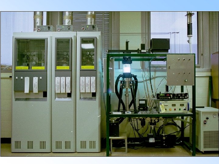
CVD - Chemical Vapor Deposition Radicals and other reactive species are formed in the mixture of methane and hydrogen. They diffuse to the surface of growing diamond layer. They react at the surface and deposits in the form of diamond. High hydrogen atom concentration prevents the formation of sp 2 carbon species. Mechanism is not fully understood as yet Boron doping from solid (boron nitride) or gaseous (boranes, B 2 H 6) sources

Boron doped diamond film electrode CVD - Chemical Vapor Deposition

BDDFE
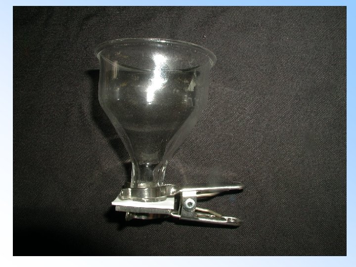
 Legend 1. 2. 3. 4. 5. 6. 7.")
Boron doped diamond film electrode (BDDFE) Legend 1. 2. 3. 4. 5. 6. 7. 8. Electrode body Screw contact Screw attachment Small metal spring Brassy sheet DFE on Si (1, 1, 1) Silicone seal Access for solution Surface of nanocrystalline diamond film electrode on Si
, copper wire (2), conductive epoxide resin (3), non-conductive epoxide resin")
BDDFE Glass tube (1), copper wire (2), conductive epoxide resin (3), non-conductive epoxide resin (4), silica wafer covered with BDDF (5), diameter of BDDFE (d, 3 mm), surface of BDDFE (A, 7, 1 mm 2).
, copper wire (2), conductive epoxide resin (3), non-conductive epoxide resin")
BDDFE Glass tube (1), copper wire (2), conductive epoxide resin (3), non-conductive epoxide resin (4), silica wafer covered with BDDF (5) Lab made Commercial

Cyclic voltammogram of 2 -nitrophenol at BDDE, BR buffer p. H 3 E [m. V]
, 3 -AB (b), and 4 -AB (c) DPV at BDNDFE (2")
2 -AB (a), 3 -AB (b), and 4 -AB (c) DPV at BDNDFE (2 -10). 10 -7 M p. H 7 p. H 8 p. H 9

DPV at BDDFE 10 -5 M 1 -nitropyrene 1 -aminopyrene Me. OH-BR pufr p. H 3 (7: 3) Regeneration E 1 = +800 m. V, t 1 = 0, 3 s E 2 = -500 m. V, t 2 = 0, 2 s
 Me. OH-BR pufr p. H")
Pasivation 1 -AP (c = 1· 10– 4 M) Me. OH-BR pufr p. H 3 (7: 3) 11 measurements Potential span 0 až +1600 m. V +230 až +680 m. V ~ +440 m. V
 in river water Reduction Oxidation")
DPV at BDDFE of 4 -NP (µM) in river water Reduction Oxidation
. 10 -6 M , Me. OH-BR")
DPV 1 -AP at BDDFE (0 - 10). 10 -6 M , Me. OH-BR buffer p. H 3, 0 (7: 3)
. 10 -7 M , Me. OH-BR")
DPV 1 -AP at BDDFE (0 - 10). 10 -7 M , Me. OH-BR buffer p. H 3, 0 (7: 3)
 DFE(a) a GCE(b)")
BDDFE detector TL arrangement 1‑AN a 1‑AB (5. 10 -6 M) DFE(a) a GCE(b)

Elektrochemical wall-jet detector with BDDFE WE Counter electrode Reference electrode

FIA-ED or HPLC-ED TL BDDFE Reference electrode Outlet rubber gasket working electrode rubber backing Inlet Kel-f body, top piece metal backing - current collector Kel-f body, bottom piece screw clamp

BDDF microelectrodes

BDDF microelectrodes
. 10 ( Me. OH: 0, 05")
-7 M HPLC-ED-BDDFE - 1 -AP (0 -10). 10 ( Me. OH: 0, 05 M Ph. B p. H 5, 0 (80: 20), E = 1000 m. V, v = 1, 0 ml/min t. R = 2, 76 min
. 10 ( Me. OH: 0, 05")
-7 M HPLC-ED-BDDFE - 1 -HP (0 -10). 10 ( Me. OH: 0, 05 M Ph. B p. H 5, 0 (80: 20), E = 1000 m. V, v = 0, 8 ml/min t. R = 3, 93 min
. 10 -8 M Me.")
HPLC-ED-BDDFE 1 -AP in urine after SPE (0 - 10). 10 -8 M Me. OH: 0, 05 M Ph. B p. H (80: 20), E = 1000 m. V, v =1, 0 ml/min
. 10 -8 M Me.")
HPLC-ED-BDDFE 1 -HP in urine after SPE (0 - 10). 10 -8 M Me. OH: 0, 05 M Ph. B p. H (80: 20), E = 1000 m. V, v =0, 8 ml/min

Thank you for your attention

- Slides: 34