Understanding and Protecting Against Electrical Overstress EOS of
- Slides: 43

Understanding and Protecting Against Electrical Overstress (EOS) of Operational-Amplifiers By Thomas Kuehl – Senior Applications Engineer Precision Analog – Linear Applications Engineering

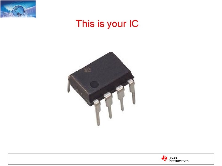
This is your IC

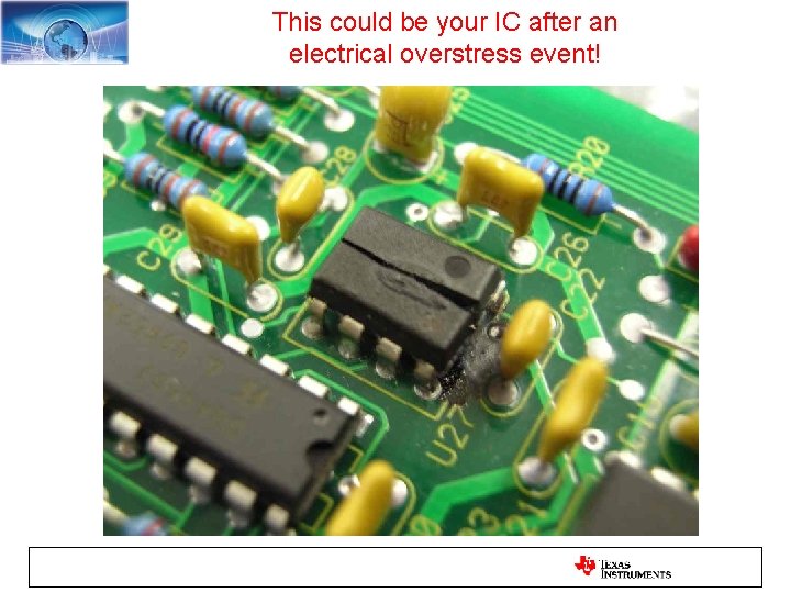
This could be your IC after an electrical overstress event!

Presentation Subjects • ESD and EOS definitions • Amplifier input range • ESD models • Internal ESD and consequently EOS protection circuits • Amplifier EOS operating situations • External EOS protection

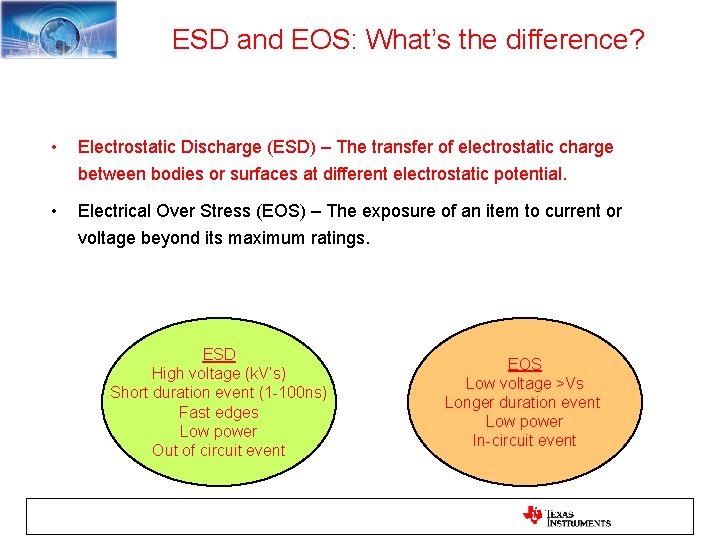
ESD and EOS: What’s the difference? • Electrostatic Discharge (ESD) – The transfer of electrostatic charge between bodies or surfaces at different electrostatic potential. • Electrical Over Stress (EOS) – The exposure of an item to current or voltage beyond its maximum ratings. ESD High voltage (k. V’s) Short duration event (1 -100 ns) Fast edges Low power Out of circuit event EOS Low voltage >Vs Longer duration event Low power In-circuit event

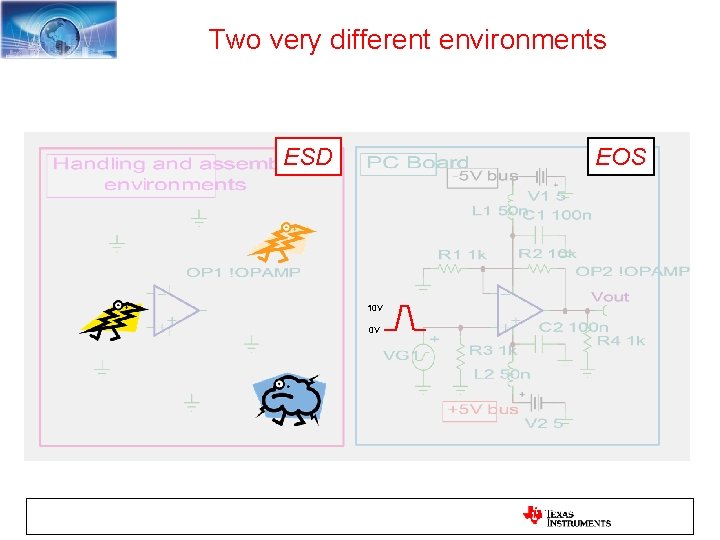
Two very different environments ESD EOS 10 V 0 V

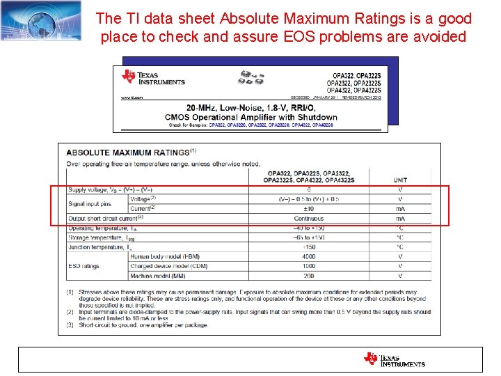
The TI data sheet Absolute Maximum Ratings is a good place to check and assure EOS problems are avoided

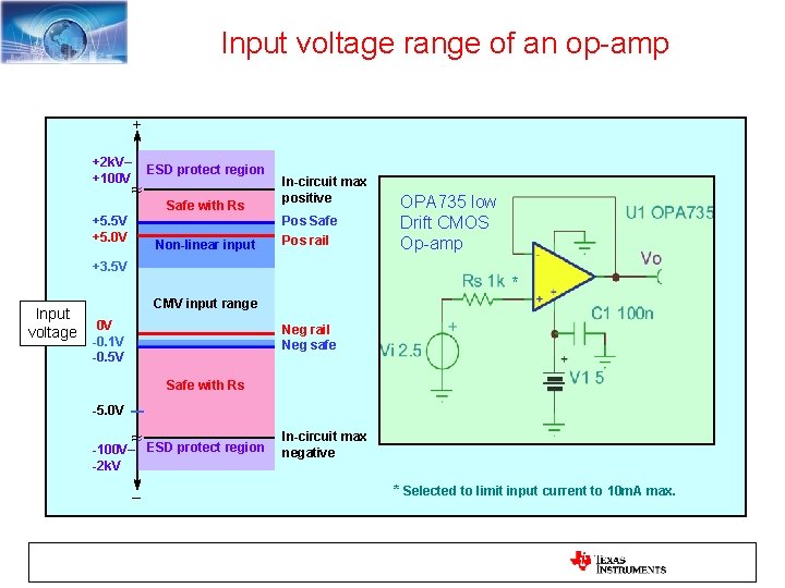
Input voltage range of an op-amp + +2 k. V– +100 V ESD protect region ≈ +5. 5 V +5. 0 V Safe with Rs Non-linear input In-circuit max positive Pos Safe Pos rail +3. 5 V Input voltage OPA 735 low Drift CMOS Op-amp * CMV input range 0 V -0. 1 V -0. 5 V Neg rail Neg safe Safe with Rs -5. 0 V ≈ -100 V– ESD protect region -2 k. V _ In-circuit max negative * Selected to limit input current to 10 m. A max.

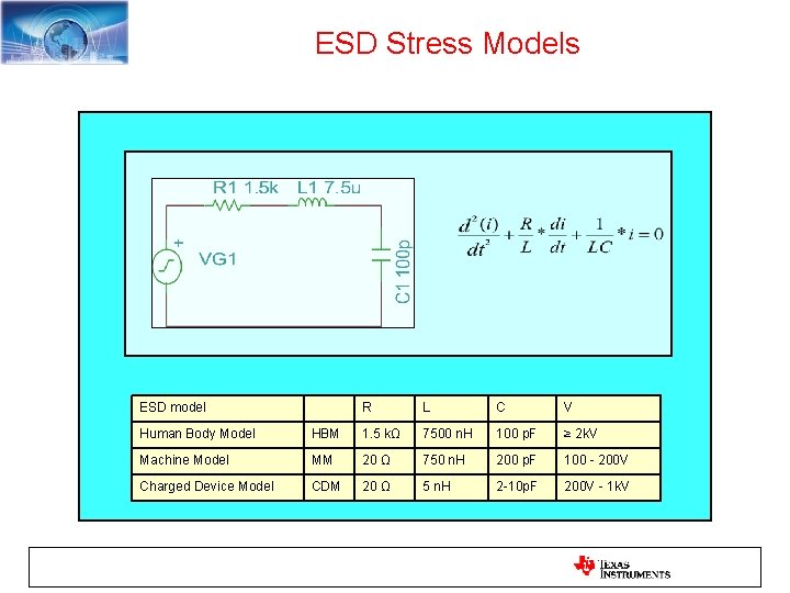
ESD Stress Models ESD model R L C V Human Body Model HBM 1. 5 kΩ 7500 n. H 100 p. F ≥ 2 k. V Machine Model MM 20 Ω 750 n. H 200 p. F 100 - 200 V Charged Device Model CDM 20 Ω 5 n. H 2 -10 p. F 200 V - 1 k. V

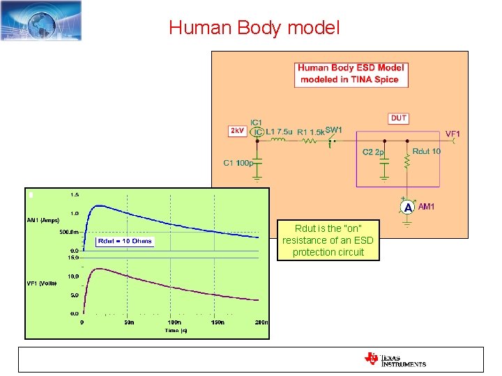
Human Body model Rdut is the “on” resistance of an ESD protection circuit

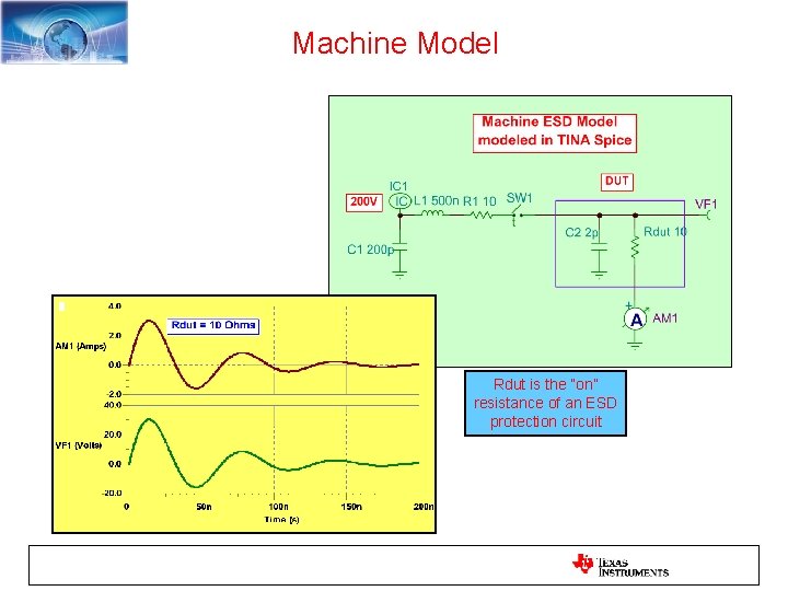
Machine Model Rdut is the “on” resistance of an ESD protection circuit

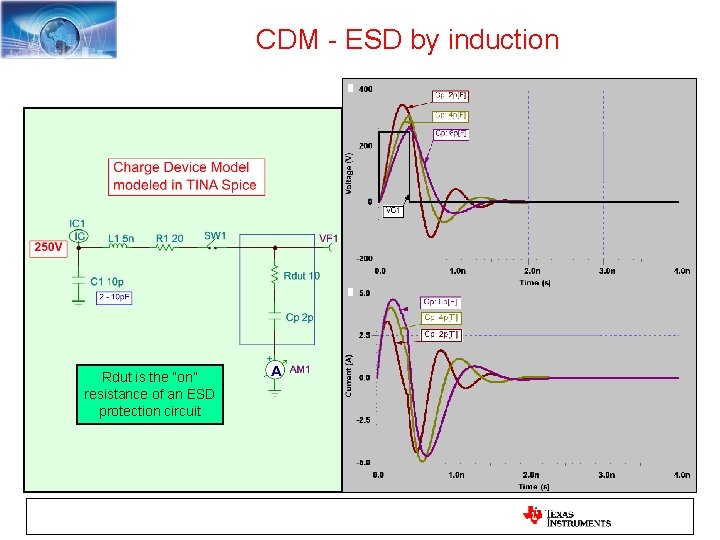
CDM - ESD by induction Rdut is the “on” resistance of an ESD protection circuit

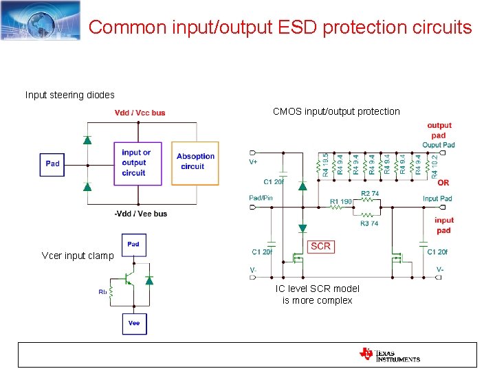
Common input/output ESD protection circuits Input steering diodes CMOS input/output protection Vcer input clamp IC level SCR model is more complex

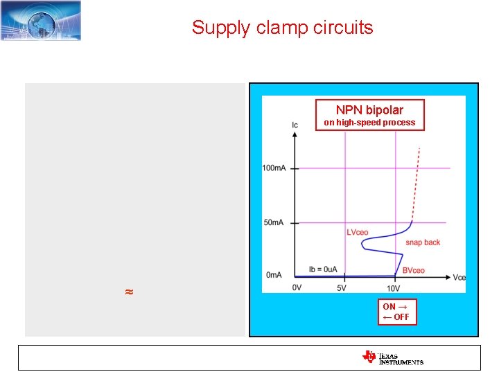
Supply clamp circuits NPN bipolar on high-speed process ≈ ON → ← OFF

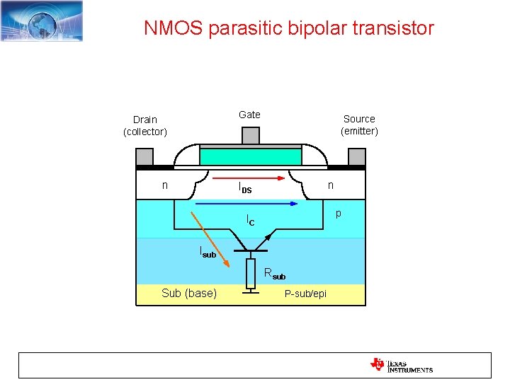
NMOS parasitic bipolar transistor Gate Drain (collector) n Source (emitter) n IDS p IC Isub Rsub Sub (base) P-sub/epi

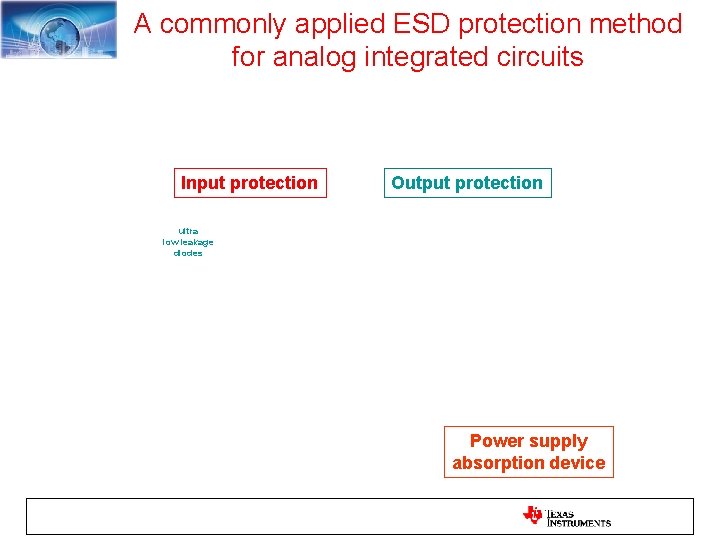
A commonly applied ESD protection method for analog integrated circuits Input protection Output protection ultra low leakage diodes Power supply absorption device

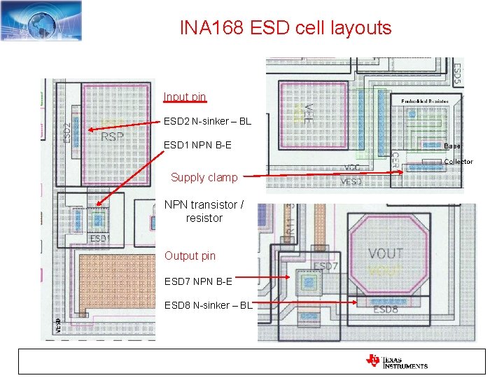
INA 168 ESD cell layouts Input pin ESD 2 N-sinker – BL ESD 1 NPN B-E Supply clamp NPN transistor / resistor Output pin ESD 7 NPN B-E ESD 8 N-sinker – BL

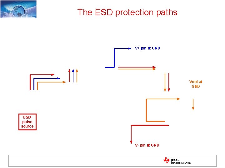
The ESD protection paths V+ pin at GND Vout at GND ESD pulse source V- pin at GND

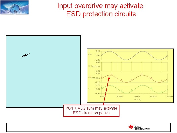
Input overdrive may activate ESD protection circuits VG 1 + VG 2 sum may activate ESD circuit on peaks

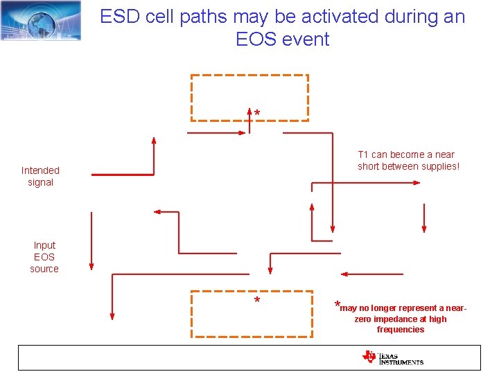
ESD cell paths may be activated during an EOS event * T 1 can become a near short between supplies! Intended signal Input EOS source * *may no longer represent a nearzero impedance at high frequencies

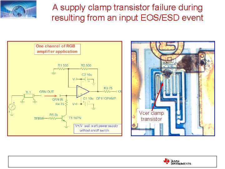
A supply clamp transistor failure during resulting from an input EOS/ESD event Vcer clamp transistor

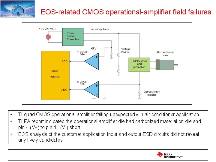
EOS-related CMOS operational-amplifier field failures • • • TI quad CMOS operational amplifier failing unexpectedly in air conditioner application TI FA report indicated the operational amplifier die had carbonized material on die and pin 4 (V+) to pin 11 (V-) short EOS analysis of the customer application input and output ESD circuits did not reveal any likely candidates

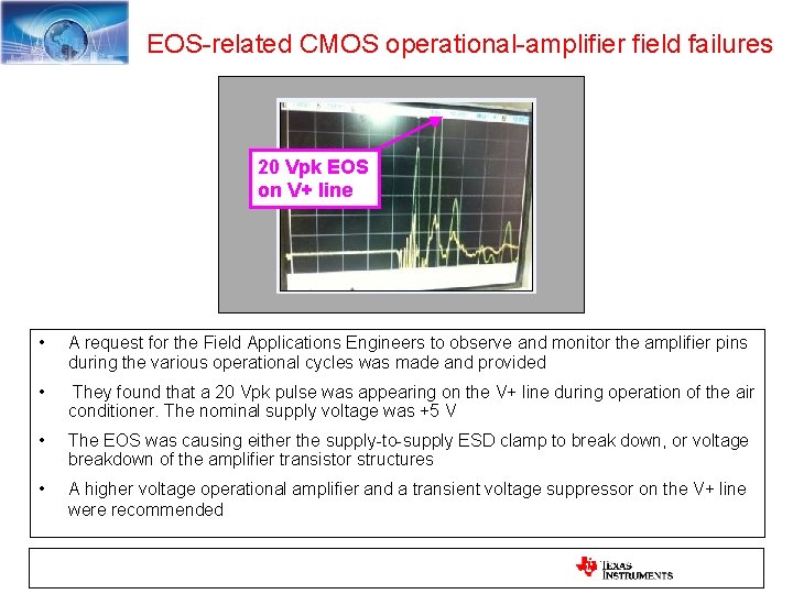
EOS-related CMOS operational-amplifier field failures 20 Vpk EOS on V+ line • A request for the Field Applications Engineers to observe and monitor the amplifier pins during the various operational cycles was made and provided • They found that a 20 Vpk pulse was appearing on the V+ line during operation of the air conditioner. The nominal supply voltage was +5 V • The EOS was causing either the supply-to-supply ESD clamp to break down, or voltage breakdown of the amplifier transistor structures • A higher voltage operational amplifier and a transient voltage suppressor on the V+ line were recommended

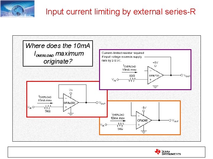
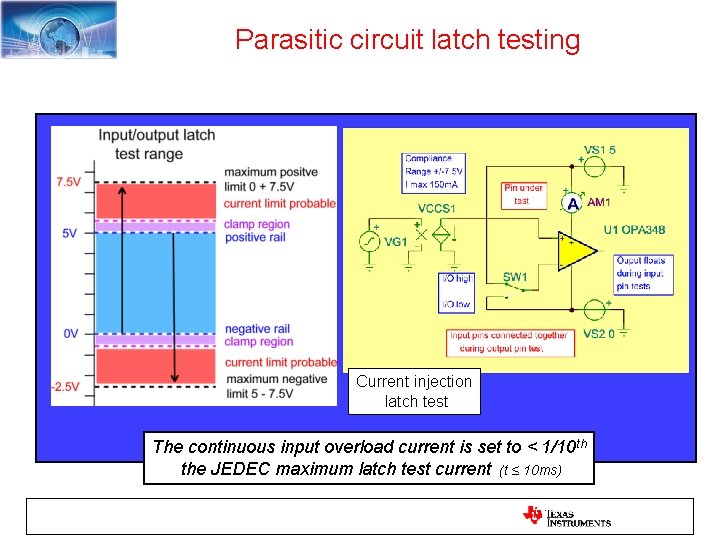
Input current limiting by external series-R Where does the 10 m. A IOVERLOAD maximum originate?

Parasitic circuit latch testing Current injection latch test The continuous input overload current is set to < 1/10 th the JEDEC maximum latch test current (t ≤ 10 ms)

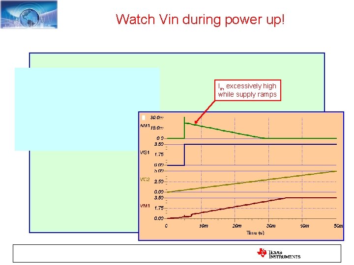
Watch Vin during power up! Iin excessively high while supply ramps

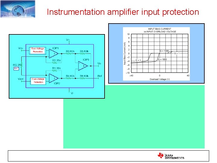
Instrumentation amplifier input protection

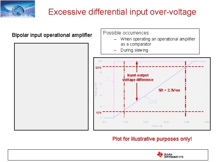
Excessive differential input over-voltage Possible occurrences Bipolar input operational amplifier – When operating an operational amplifier as a comparator – During slewing 90% Input-output voltage difference SR = 2. 3 V/us 10% Plot for illustrative purposes only!

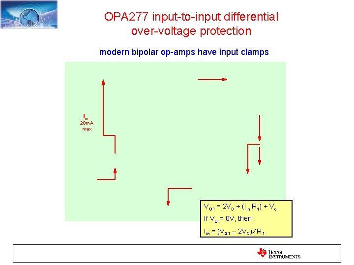
OPA 277 input-to-input differential over-voltage protection modern bipolar op-amps have input clamps Iin 20 m. A max VG 1 = 2 VD + (Iin R 1) + Vo If VO = 0 V, then: Iin = (VG 1 – 2 VD) ∕ R 1

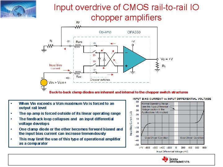
Input overdrive of CMOS rail-to-rail IO chopper amplifiers Back-to-back clamp diodes are inherent and internal to the chopper switch structures • • • When Vin exceeds a Vcm maximum Vo is forced to an output rail level The op-amp is forced outside of its linear operating range The feedback loop collapses and an input differential voltage develops One clamp diode or the other becomes forward biased and the input bias current can increase tremendously This may limit the use of this type of operational amplifier as a comparator

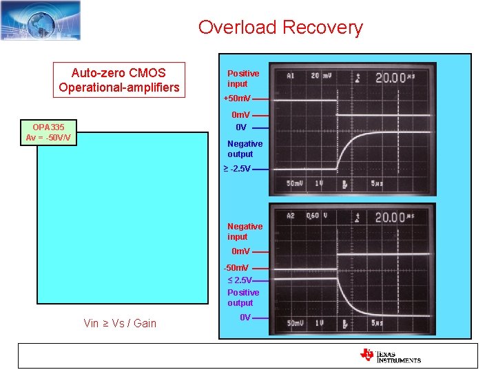
Overload Recovery Auto-zero CMOS Operational-amplifiers Positive input +50 m. V 0 V OPA 335 Av = -50 V/V Negative output ≥ -2. 5 V Negative input 0 m. V -50 m. V ≤ 2. 5 V Positive output Vin ≥ Vs / Gain 0 V

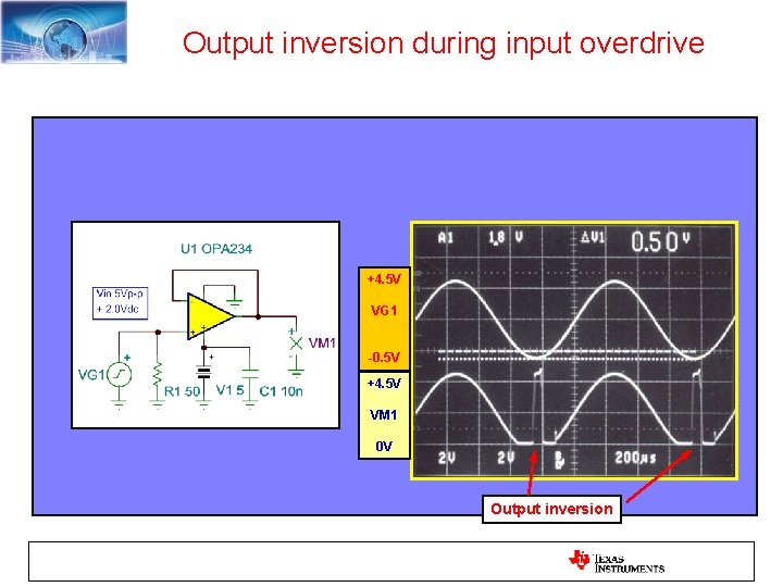
Output inversion during input overdrive +4. 5 V VG 1 -0. 5 V +4. 5 V VM 1 0 V Output inversion

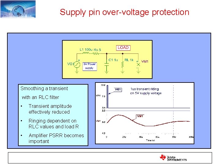
Supply pin over-voltage protection Smoothing a transient with an RLC filter • Transient amplitude effectively reduced • Ringing dependent on RLC values and load R • Amplifier PSRR becomes important

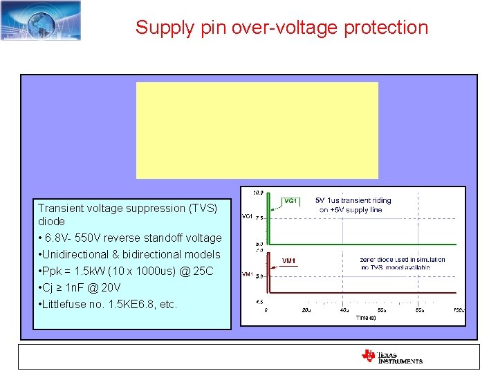
Supply pin over-voltage protection Transient voltage suppression (TVS) diode • 6. 8 V- 550 V reverse standoff voltage • Unidirectional & bidirectional models • Ppk = 1. 5 k. W (10 x 1000 us) @ 25 C • Cj ≥ 1 n. F @ 20 V • Littlefuse no. 1. 5 KE 6. 8, etc.

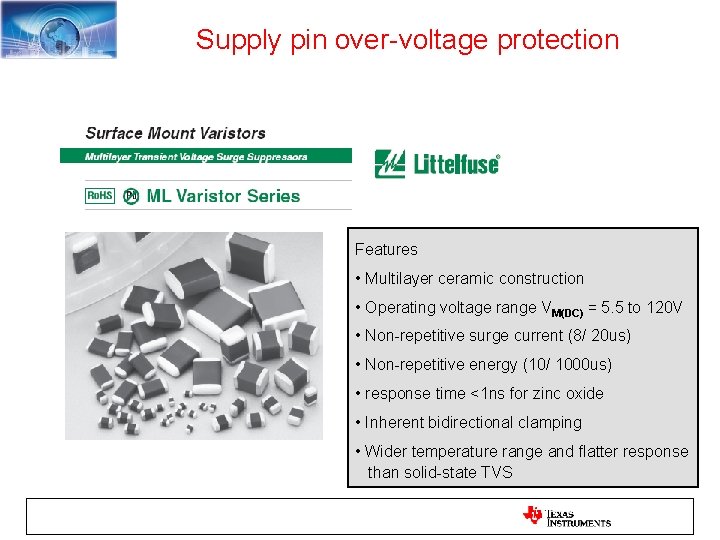
Supply pin over-voltage protection Features • Multilayer ceramic construction • Operating voltage range VM(DC) = 5. 5 to 120 V • Non-repetitive surge current (8/ 20 us) • Non-repetitive energy (10/ 1000 us) • response time <1 ns for zinc oxide • Inherent bidirectional clamping • Wider temperature range and flatter response than solid-state TVS

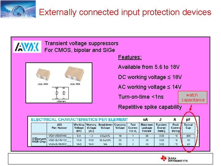
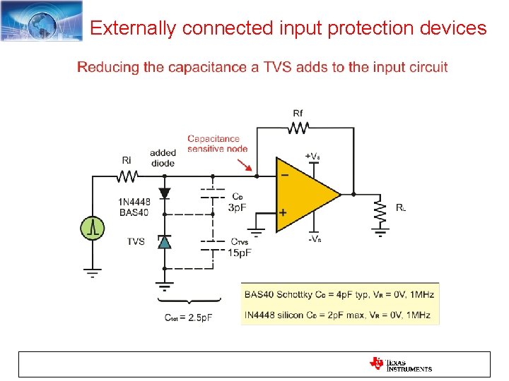
Externally connected input protection devices Transient voltage suppressors For CMOS, bipolar and Si. Ge Features: Available from 5. 6 to 18 V DC working voltage ≤ 18 V AC working voltage ≤ 14 V watch capacitance Turn-on-time <1 ns Repetitive spike capability u. A J A p. F

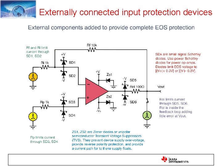
Externally connected input protection devices

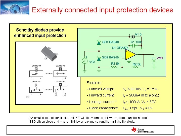
Externally connected input protection devices Schottky diodes provide enhanced input protection Features: • Forward voltage VF ≤ 380 m. V, IF = 1 m. A • Forward current IF = 200 m. A max (cont. ) • Leakage current * IR ≤ 100 n. A, VR = 30 V • Diode capacitance Ctot ≤ 5 p. F, VR = 0 V * A small-signal silicon diode (IN 4148) will likely turn on at lower voltage than the internal ESD silicon diode and may exhibit lower leakage current than a Schottky diode.

Externally connected input protection devices

An important point about added protection devices in the signal circuit • Protection components such as transient voltage suppressors (TVS), diodes and zener diodes all exhibit capacitance even when biased off • The capacitance will vary to some extent with the voltage applied across the protection device • Most often the capacitance does not have a linear capacitance to voltage relationship (voltage coefficient) • This non-linear capacitance to voltage relationship may increase distortion in the protected circuit • It will be most evident in a very low THD circuits, but may not degrade performance significantly

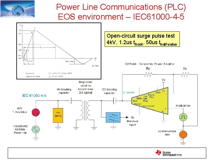
Power Line Communications (PLC) EOS environment – IEC 61000 -4 -5 Open-circuit surge pulse test 4 k. V, 1. 2 us tfront, 50 us thalf-value

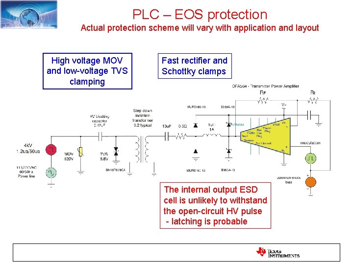
PLC – EOS protection Actual protection scheme will vary with application and layout High voltage MOV and low-voltage TVS clamping Fast rectifier and Schottky clamps The internal output ESD cell is unlikely to withstand the open-circuit HV pulse - latching is probable

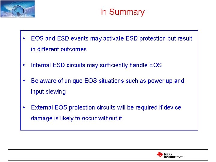
In Summary • EOS and ESD events may activate ESD protection but result in different outcomes • Internal ESD circuits may sufficiently handle EOS • Be aware of unique EOS situations such as power up and input slewing • External EOS protection circuits will be required if device damage is likely to occur without it