Ultralow Power Components for a 94 GHz Transceiver

- Slides: 36

Ultra-low Power Components for a 94 GHz Transceiver Seong-Kyun Kim 1, Robert Maurer 1, Arda Simsek 1, Miguel Urteaga 2, and Mark. J. W. Rodwell 1 1 University of California at Santa Barbara, CA 2 Teledyne Scientific and Imaging, CA CSICS 2016 Austin, TX

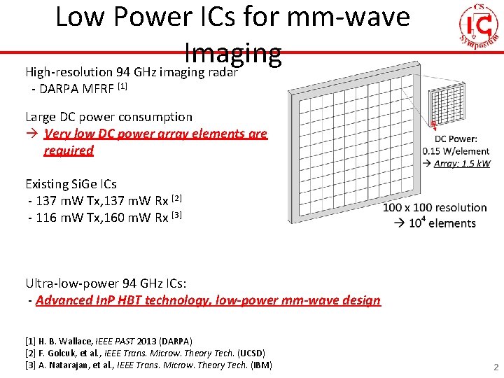
Low Power ICs for mm-wave Imaging High-resolution 94 GHz imaging radar - DARPA MFRF [1] Large DC power consumption Very low DC power array elements are required Existing Si. Ge ICs - 137 m. W Tx, 137 m. W Rx [2] - 116 m. W Tx, 160 m. W Rx [3] Ultra-low-power 94 GHz ICs: - Advanced In. P HBT technology, low-power mm-wave design [1] H. B. Wallace, IEEE PAST 2013 (DARPA) [2] F. Golcuk, et al. , IEEE Trans. Microw. Theory Tech. (UCSD) [3] A. Natarajan, et al. , IEEE Trans. Microw. Theory Tech. (IBM) 2

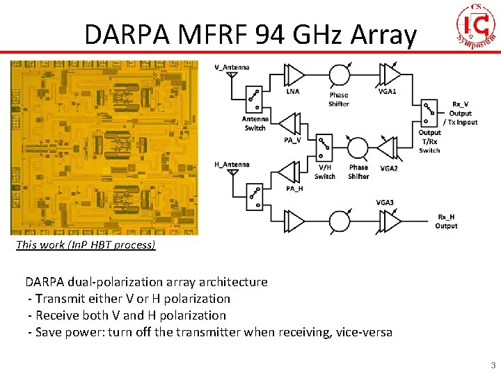
DARPA MFRF 94 GHz Array This work (In. P HBT process) DARPA dual-polarization array architecture - Transmit either V or H polarization - Receive both V and H polarization - Save power: turn off the transmitter when receiving, vice-versa 3

THz HBTs (Teledyne) for Low Power 1. 1 THz fmax In. P HBTs high gain per stage with low power Low-power (1 V, 1 m. A) bias, 0. 13 x 3 μm 2 HBT - 16. 8 d. B common base @ 1 m. W DC 16. 8 d. B/m. W - 10. 4 d. B common emitter @ 1 m. W DC 10. 4 d. B/m. W 4

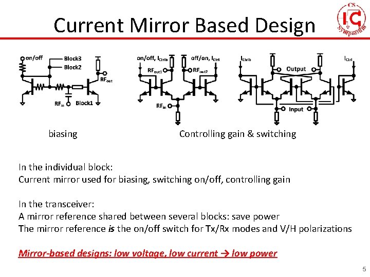
Current Mirror Based Design biasing Controlling gain & switching In the individual block: Current mirror used for biasing, switching on/off, controlling gain In the transceiver: A mirror reference shared between several blocks: save power The mirror reference is the on/off switch for Tx/Rx modes and V/H polarizations Mirror-based designs: low voltage, low current → low power 5

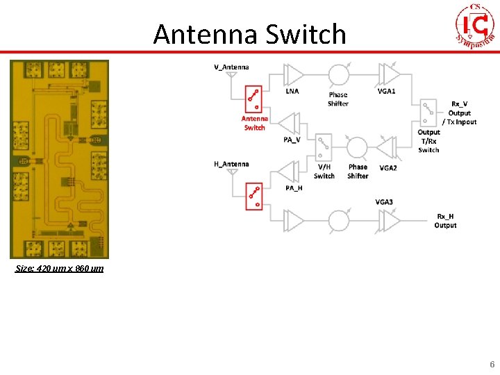
Antenna Switch Size: 420 um x 860 um 6

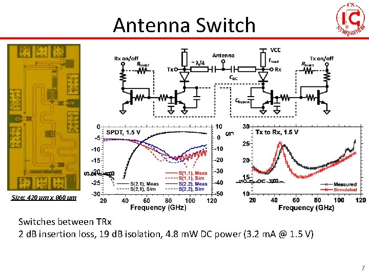
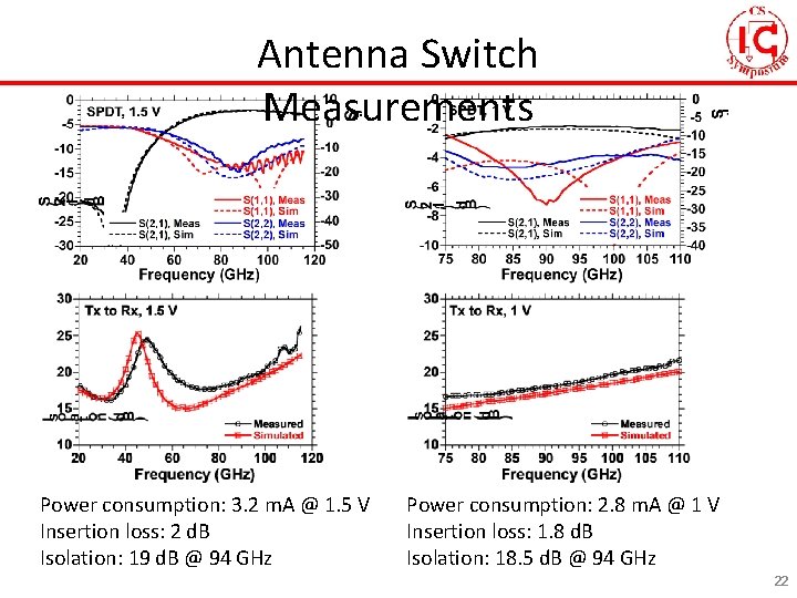
Antenna Switch Size: 420 um x 860 um Switches between TRx 2 d. B insertion loss, 19 d. B isolation, 4. 8 m. W DC power (3. 2 m. A @ 1. 5 V) 7

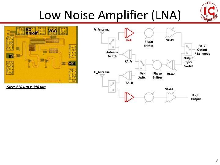
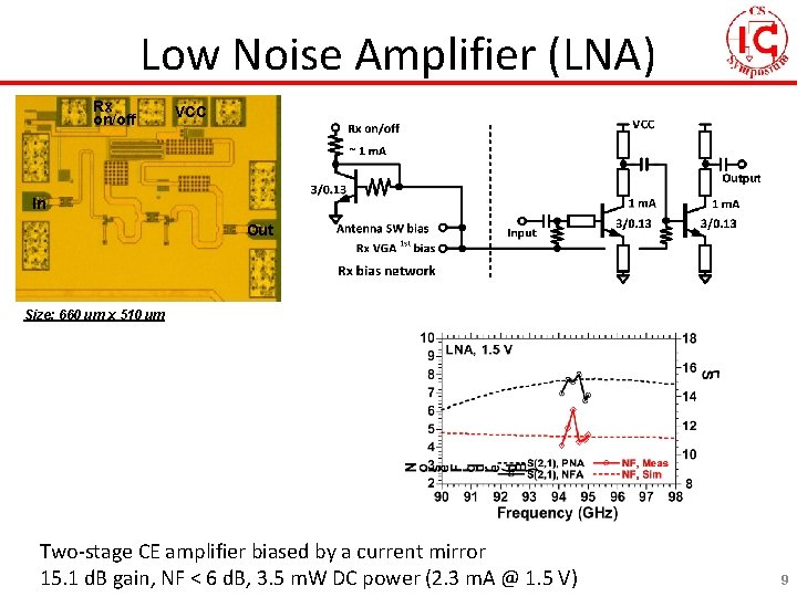
Low Noise Amplifier (LNA) Rx on/off VCC In Out Size: 660 um x 510 um 8

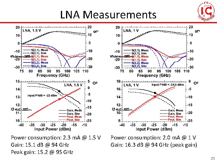
Low Noise Amplifier (LNA) Rx on/off VCC In Out Size: 660 um x 510 um Two-stage CE amplifier biased by a current mirror 15. 1 d. B gain, NF < 6 d. B, 3. 5 m. W DC power (2. 3 m. A @ 1. 5 V) 9

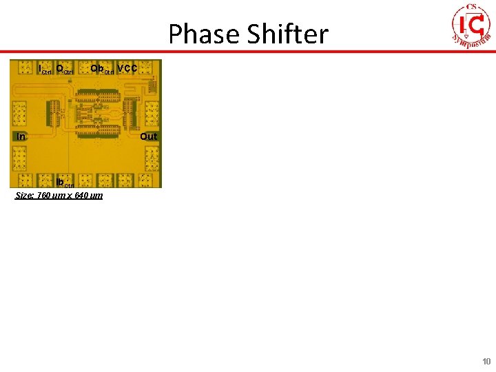
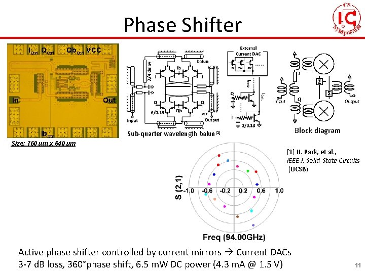
Phase Shifter ICtrl Qb. Ctrl VCC In Out Ib. Ctrl Size: 760 um x 640 um 10

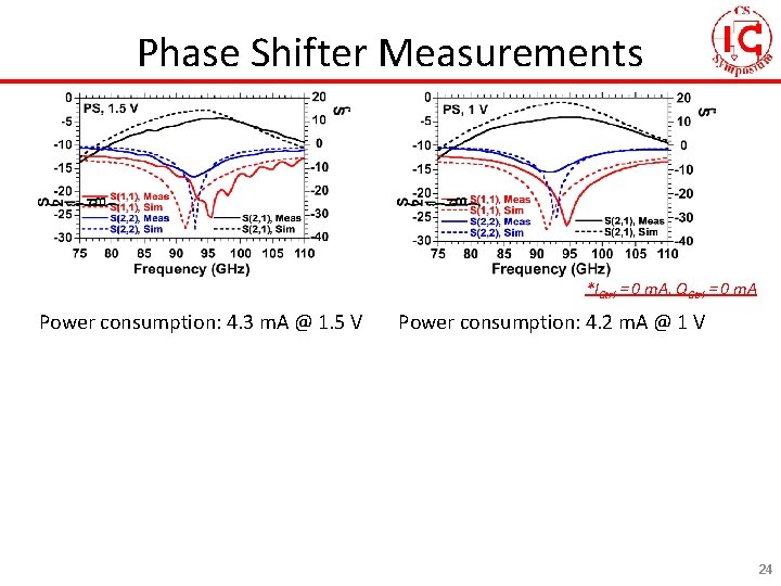
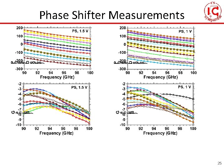
Phase Shifter ICtrl Qb. Ctrl VCC In Out Ib. Ctrl Block diagram Sub-quarter wavelength balun[1] Size: 760 um x 640 um [1] H. Park, et al. , IEEE J. Solid-State Circuits (UCSB) Active phase shifter controlled by current mirrors Current DACs 3 -7 d. B loss, 360°phase shift, 6. 5 m. W DC power (4. 3 m. A @ 1. 5 V) 11

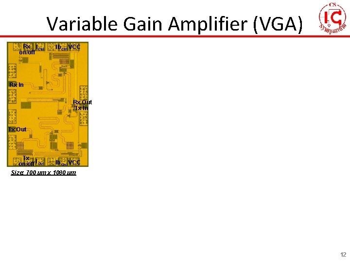
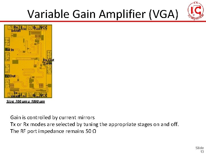
Variable Gain Amplifier (VGA) Rx ICtrl on/off Ib. Ctrl VCC Rx In Rx Out /Tx In Tx Out Tx Ib. Ctrl VCC on/off ICtrl Size: 700 um x 1080 um 12

Variable Gain Amplifier (VGA) Rx ICtrl on/off Ib. Ctrl VCC Rx In Rx Out /Tx In Tx Out Tx Ib. Ctrl VCC on/off ICtrl Size: 700 um x 1080 um Gain is controlled by current mirrors Tx or Rx modes are selected by tuning the appropriate stages on and off. The RF port impedance remains 50 Ω Slide 13

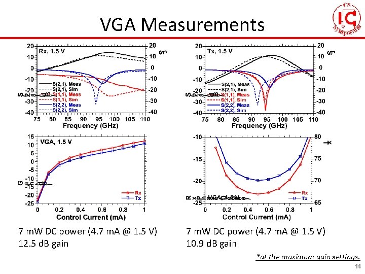
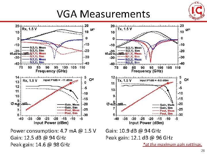
VGA Measurements 7 m. W DC power (4. 7 m. A @ 1. 5 V) 12. 5 d. B gain 7 m. W DC power (4. 7 m. A @ 1. 5 V) 10. 9 d. B gain *at the maximum gain settings. 14

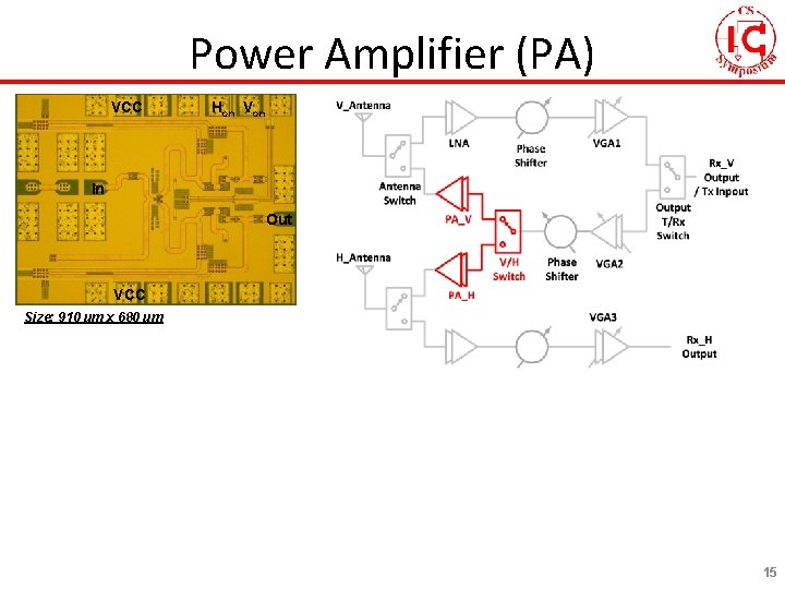
Power Amplifier (PA) VCC Hon Von In Out VCC Size: 910 um x 680 um 15

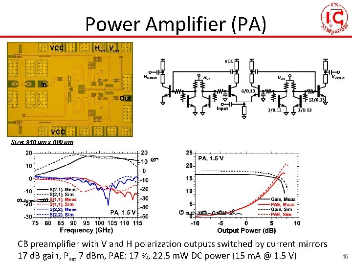
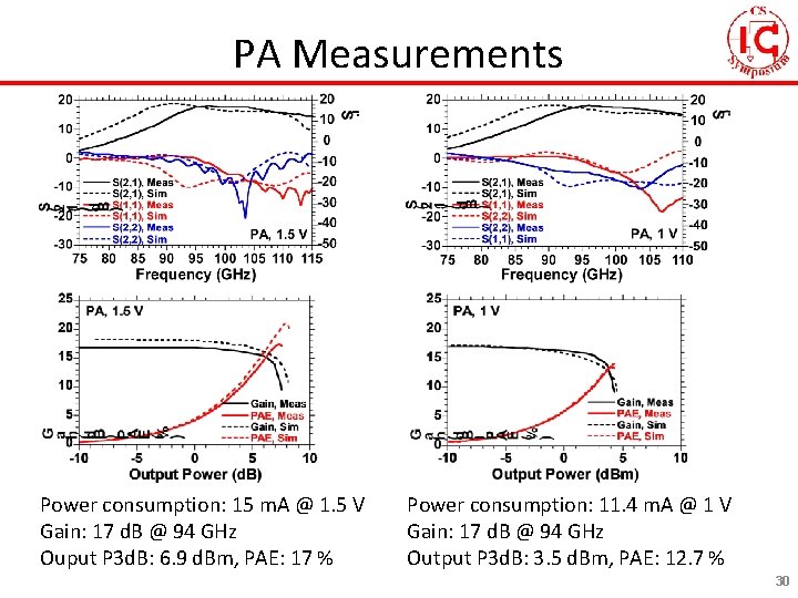
Power Amplifier (PA) VCC Hon Von In Out VCC Size: 910 um x 680 um CB preamplifier with V and H polarization outputs switched by current mirrors 17 d. B gain, Psat 7 d. Bm, PAE: 17 %, 22. 5 m. W DC power (15 m. A @ 1. 5 V) 16

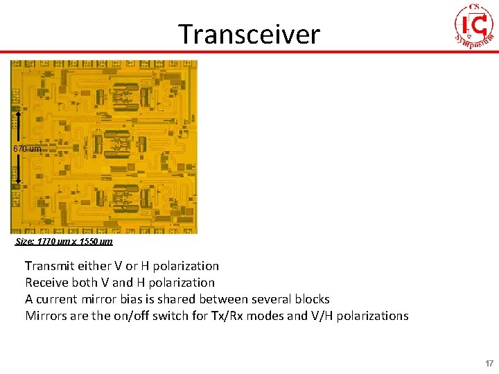
Transceiver 670 um Size: 1770 um x 1550 um Transmit either V or H polarization Receive both V and H polarization A current mirror bias is shared between several blocks Mirrors are the on/off switch for Tx/Rx modes and V/H polarizations 17

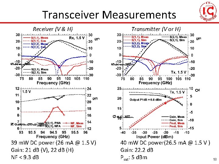
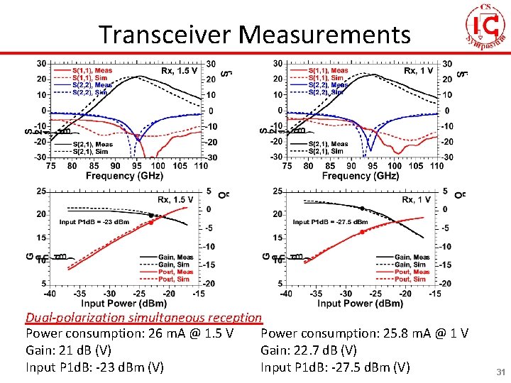
Transceiver Measurements Receiver (V & H) 39 m. W DC power (26 m. A @ 1. 5 V) Gain: 21 d. B (V), 22 d. B (H) NF < 9. 3 d. B Transmitter (V or H) 40 m. W DC power(26. 5 m. A @ 1. 5 V ) Gain: 22. 2 d. B Psat: 5 d. Bm 18

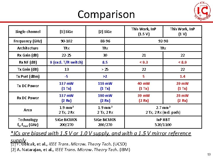
Comparison This Work, In. P (1. 5 V) This Work, In. P (1 V) Single-channel [1] Si. Ge [2] Si. Ge Frequency (GHz) 90 -102 88 -96 92 -98 Architecture TRx TRx Rx Gain (d. B) 22 -25 30 21 22 Rx NF (d. B) 9 (excl. T/R switch) 8. 5 < 9. 3 < 8. 9 Tx Gain (d. B) 13 > 25 22 22 Tx Psat (d. Bm) -5 >2 5 1. 4 Tx DC Power 137 m. W (1 Tx) 116 m. W (1 Tx) 40 m. W (1 Tx) 29 m. W (1 Tx) Rx DC Power 137 m. W (2 Rx) 160 m. W (2 Rx) 39 m. W (2 Rx) 26 m. W (2 Rx) Area 1. 9 mm 2 2 Tx, 2 Rx 2. 7 mm 2 2 Tx, 2 Rx (incl. pads) Technology fτ, fmax (GHz) Si. Ge Bi. CMOS 200/270 In. P HBT 520/1100 *ICs are biased with 1. 5 V or 1. 0 V supply, and with a 1. 5 V mirror reference supply [1] F. Golcuk, et al. , IEEE Trans. Microw. Theory Tech. (UCSD) [2] A. Natarajan, et al. , IEEE Trans. Microw. Theory Tech. (IBM) 19

Ultra-Low Power Array Components Ultra low power components and a transceiver for a 94 GHz dual-polarization phased-array NF < 9. 3 d. B, Psat > 1. 4 d. Bm with low DC power 1. 5 V bias: 40 m. W receiver (V & H), 39 m. W transmitter (V or H), 1. 0 V bias: 29 m. W receiver (V & H), 26 m. W transmitter (V or H) Low power by: 1. 1 THz In. P HBTs Current-mirror-based mm-wave IC design We thank Teledyne Scientific & Imaging for IC fabrication. 20

Thank you

Antenna Switch Measurements Power consumption: 3. 2 m. A @ 1. 5 V Insertion loss: 2 d. B Isolation: 19 d. B @ 94 GHz Power consumption: 2. 8 m. A @ 1 V Insertion loss: 1. 8 d. B Isolation: 18. 5 d. B @ 94 GHz 22

LNA Measurements Power consumption: 2. 3 m. A @ 1. 5 V Gain: 15. 1 d. B @ 94 GHz Peak gain: 15. 2 @ 95 GHz Power consumption: 2. 0 m. A @ 1 V Gain: 16. 3 d. B @ 94 GHz (peak gain) 23

Phase Shifter Measurements *ICtrl = 0 m. A, QCtrl = 0 m. A Power consumption: 4. 3 m. A @ 1. 5 V Power consumption: 4. 2 m. A @ 1 V 24

Phase Shifter Measurements 25

VGA Measurements Power consumption: 4. 7 m. A @ 1. 5 V Gain: 12. 5 d. B @ 94 GHz Peak gain: 14. 6 @ 98 GHz Gain: 10. 9 d. B @ 94 GHz Peak gain: 12. 1 d. B @ 96 GHz *at the maximum gain settings. 26

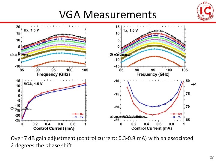
VGA Measurements Over 7 d. B gain adjustment (control current: 0. 3 -0. 8 m. A) with an associated 2 degrees the phase shift 27

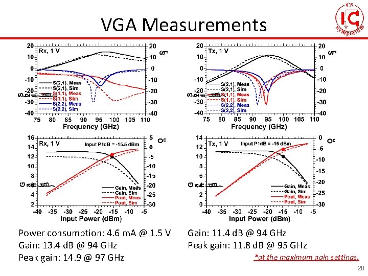
VGA Measurements Power consumption: 4. 6 m. A @ 1. 5 V Gain: 13. 4 d. B @ 94 GHz Peak gain: 14. 9 @ 97 GHz Gain: 11. 4 d. B @ 94 GHz Peak gain: 11. 8 d. B @ 95 GHz *at the maximum gain settings. 28

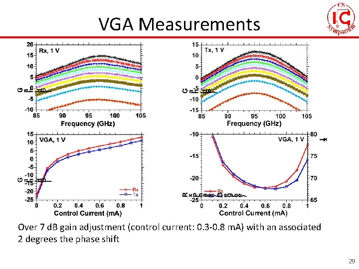
VGA Measurements Over 7 d. B gain adjustment (control current: 0. 3 -0. 8 m. A) with an associated 2 degrees the phase shift 29

PA Measurements Power consumption: 15 m. A @ 1. 5 V Gain: 17 d. B @ 94 GHz Ouput P 3 d. B: 6. 9 d. Bm, PAE: 17 % Power consumption: 11. 4 m. A @ 1 V Gain: 17 d. B @ 94 GHz Output P 3 d. B: 3. 5 d. Bm, PAE: 12. 7 % 30

Transceiver Measurements Dual-polarization simultaneous reception Power consumption: 26 m. A @ 1. 5 V Power consumption: 25. 8 m. A @ 1 V Gain: 21 d. B (V) Gain: 22. 7 d. B (V) Input P 1 d. B: -23 d. Bm (V) Input P 1 d. B: -27. 5 d. Bm (V) 31

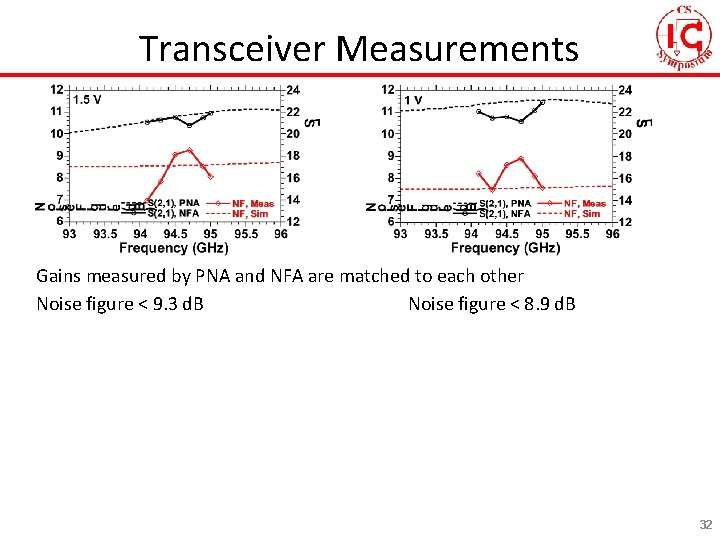
Transceiver Measurements Gains measured by PNA and NFA are matched to each other Noise figure < 9. 3 d. B Noise figure < 8. 9 d. B 32

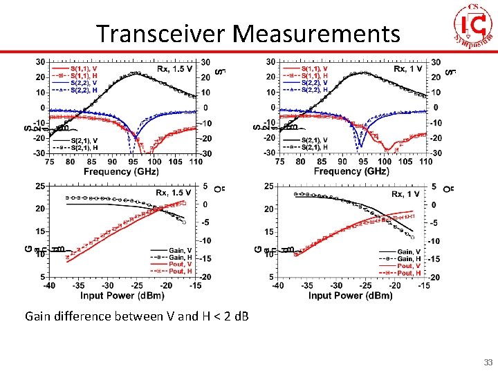
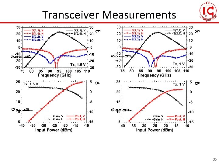
Transceiver Measurements Gain difference between V and H < 2 d. B 33

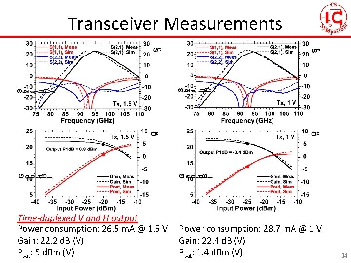
Transceiver Measurements Time-duplexed V and H output Power consumption: 26. 5 m. A @ 1. 5 V Gain: 22. 2 d. B (V) Psat: 5 d. Bm (V) Power consumption: 28. 7 m. A @ 1 V Gain: 22. 4 d. B (V) Psat: 1. 4 d. Bm (V) 34

Transceiver Measurements 35

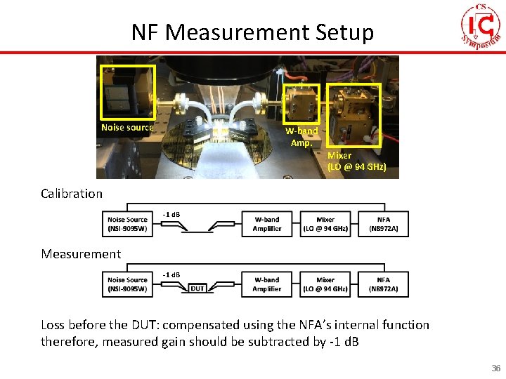
NF Measurement Setup Noise source W-band Amp. Mixer (LO @ 94 GHz) Calibration -1 d. B Measurement -1 d. B Loss before the DUT: compensated using the NFA’s internal function therefore, measured gain should be subtracted by -1 d. B 36