Ultra Low Power CMOS Design Doctoral Defense Kyungseok
![Low Power Design Using Dual-Vdd FF FF/ LCFF CVS Structure [9] MILP I LC(Level Low Power Design Using Dual-Vdd FF FF/ LCFF CVS Structure [9] MILP I LC(Level](https://slidetodoc.com/presentation_image_h/c590413c59a1a2dc32e90356f4d33d0f/image-13.jpg)
![Multiple Logic-Level Gates (Delay) Multiple Logic-Level NAND 2 [11] April 6, 2011 Multiple Logic. Multiple Logic-Level Gates (Delay) Multiple Logic-Level NAND 2 [11] April 6, 2011 Multiple Logic.](https://slidetodoc.com/presentation_image_h/c590413c59a1a2dc32e90356f4d33d0f/image-19.jpg)
![References [1] A. Wang, B. H. Calhoun, and A. P. Chandrakasan, Sub-Threshold Design for References [1] A. Wang, B. H. Calhoun, and A. P. Chandrakasan, Sub-Threshold Design for](https://slidetodoc.com/presentation_image_h/c590413c59a1a2dc32e90356f4d33d0f/image-42.jpg)

- Slides: 43

Ultra Low Power CMOS Design Doctoral Defense Kyungseok Kim ECE Dept. Auburn University Dissertation Committee: Chair: Prof. Vishwani D. Agrawal Prof. Victor P. Nelson, Prof. Fa Foster Dai Outside reader: Prof. Allen Landers April 6, 2011

Outline q Motivation q Problem Statement q Ultra-Low Power Design q Contributions of This Work q Conclusion April 6, 2011 2 K. Kim-Ph. D Defense

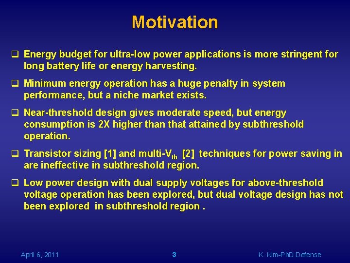
Motivation q Energy budget for ultra-low power applications is more stringent for long battery life or energy harvesting. q Minimum energy operation has a huge penalty in system performance, but a niche market exists. q Near-threshold design gives moderate speed, but energy consumption is 2 X higher than that attained by subthreshold operation. q Transistor sizing [1] and multi-Vth [2] techniques for power saving in are ineffective in subthreshold region. q Low power design with dual supply voltages for above-threshold voltage operation has been explored, but dual voltage design has not been explored in subthreshold region. April 6, 2011 3 K. Kim-Ph. D Defense

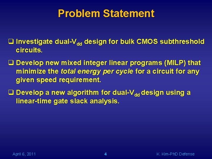
Problem Statement q Investigate dual-Vdd design for bulk CMOS subthreshold circuits. q Develop new mixed integer linear programs (MILP) that minimize the total energy per cycle for a circuit for any given speed requirement. q Develop a new algorithm for dual-Vdd design using a linear-time gate slack analysis. April 6, 2011 4 K. Kim-Ph. D Defense

Outline q Motivation q Problem Statement q Ultra-Low Power Design q Contributions of This Work q Conclusion April 6, 2011 5 K. Kim-Ph. D Defense

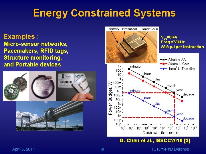
Energy Constrained Systems Examples : Vdd=0. 4 V, Freq. =73 k. Hz 28. 9 p. J per instruction Micro-sensor networks, Pacemakers RFID tags, Structure monitoring, and Portable devices G. Chen et al. , ISSCC 2010 [3] April 6, 2011 6 K. Kim-Ph. D Defense

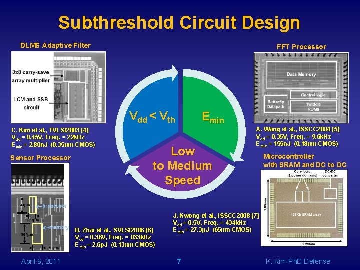
Subthreshold Circuit Design DLMS Adaptive Filter FFT Processor Vdd < Vth C. Kim et al. , TVLSI 2003 [4] Vdd = 0. 45 V, Freq. = 22 k. Hz Emin = 2. 80 n. J (0. 35 um CMOS) Sensor Processor Low to Medium Speed B. Zhai et al. , SVLSI 2006 [6] Vdd = 0. 36 V, Freq. = 833 k. Hz Emin = 2. 6 p. J (0. 13 um CMOS) April 6, 2011 Emin A. Wang et al. , ISSCC 2004 [5] Vdd = 0. 35 V, Freq. = 9. 6 k. Hz Emin = 155 n. J (0. 18 um CMOS) Microcontroller with SRAM and DC to DC J. Kwong et al. , ISSCC 2008 [7] Vdd = 0. 5 V, Freq. = 434 k. Hz Emin = 27. 3 p. J (65 nm CMOS) 7 K. Kim-Ph. D Defense

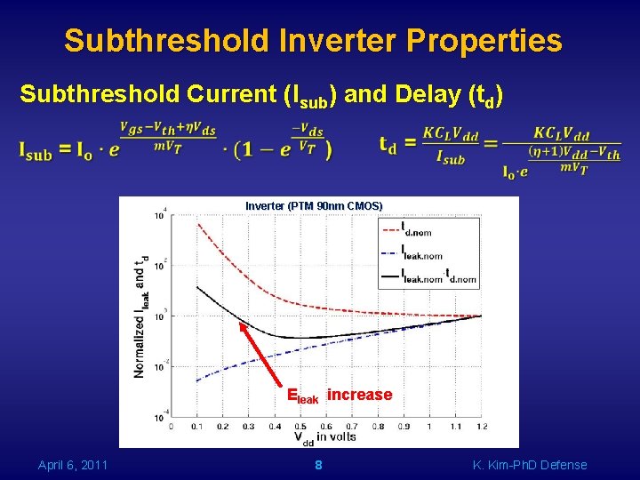
Subthreshold Inverter Properties Subthreshold Current (Isub) and Delay (td) Inverter (PTM 90 nm CMOS) Eleak increase April 6, 2011 8 K. Kim-Ph. D Defense

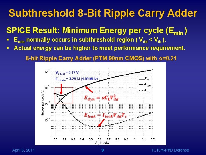
Subthreshold 8 -Bit Ripple Carry Adder SPICE Result: Minimum Energy per cycle (Emin ) § Emin normally occurs in subthreshold region ( Vdd < Vth ). § Actual energy can be higher to meet performance requirement. 8 -bit Ripple Carry Adder (PTM 90 nm CMOS) with α=0. 21 Vdd, opt = 0. 17 V Etot, min = 3. 29 f. J (1. 89 MHz) April 6, 2011 9 K. Kim-Ph. D Defense

Outline q Motivation q Problem Statement q Ultra-Low Power Design q Contributions of This Work Ø MILP I for Minimum Energy Design Using Dual-Vdd without LC q Conclusion April 6, 2011 10 K. Kim-Ph. D Defense

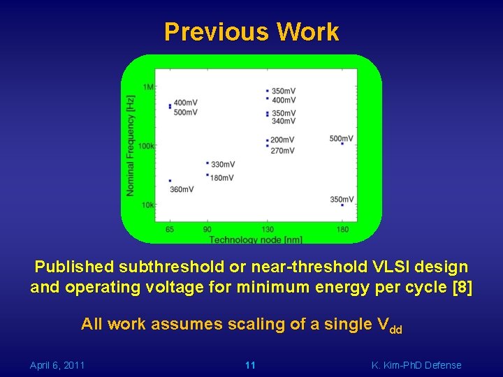
Previous Work Published subthreshold or near-threshold VLSI design and operating voltage for minimum energy per cycle [8] All work assumes scaling of a single Vdd April 6, 2011 11 K. Kim-Ph. D Defense

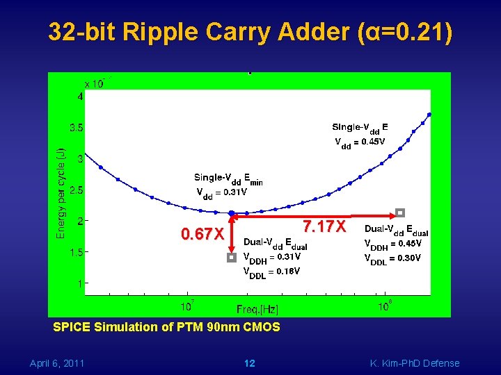
32 -bit Ripple Carry Adder (α=0. 21) 7. 17 X 0. 67 X SPICE Simulation of PTM 90 nm CMOS April 6, 2011 12 K. Kim-Ph. D Defense
![Low Power Design Using DualVdd FF FF LCFF CVS Structure 9 MILP I LCLevel Low Power Design Using Dual-Vdd FF FF/ LCFF CVS Structure [9] MILP I LC(Level](https://slidetodoc.com/presentation_image_h/c590413c59a1a2dc32e90356f4d33d0f/image-13.jpg)
Low Power Design Using Dual-Vdd FF FF/ LCFF CVS Structure [9] MILP I LC(Level Converter) FF FF/ LCFF ECVS Structure [10] MILP II VDDH VDDL April 6, 2011 13 K. Kim-Ph. D Defense

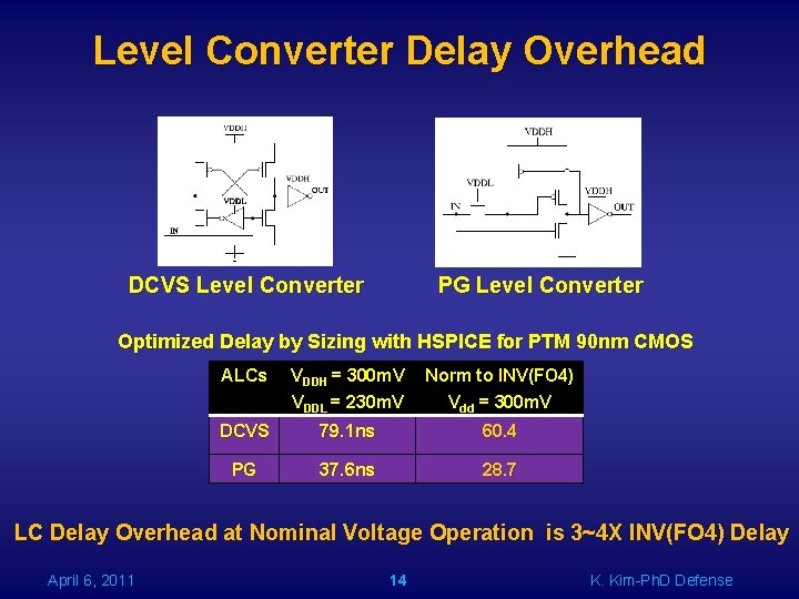
Level Converter Delay Overhead PG Level Converter DCVS Level Converter Optimized Delay by Sizing with HSPICE for PTM 90 nm CMOS ALCs VDDH = 300 m. V VDDL = 230 m. V Norm to INV(FO 4) Vdd = 300 m. V DCVS 79. 1 ns 60. 4 PG 37. 6 ns 28. 7 LC Delay Overhead at Nominal Voltage Operation is 3~4 X INV(FO 4) Delay April 6, 2011 14 K. Kim-Ph. D Defense

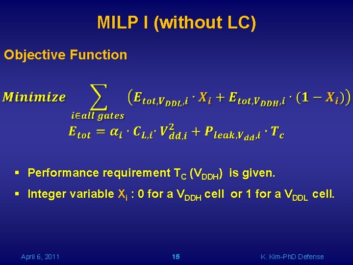
MILP I (without LC) Objective Function § Performance requirement TC (VDDH) is given. § Integer variable Xi : 0 for a VDDH cell or 1 for a VDDL cell. April 6, 2011 15 K. Kim-Ph. D Defense

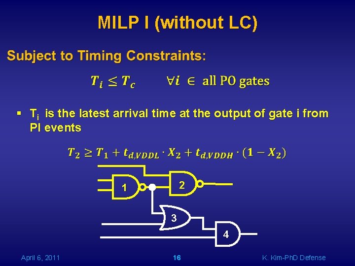
MILP I (without LC) § Ti is the latest arrival time at the output of gate i from PI events 2 1 3 4 April 6, 2011 16 K. Kim-Ph. D Defense

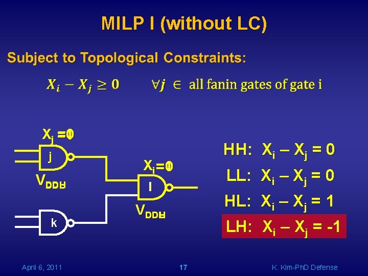
MILP I (without LC) Xj =1 =0 j VDDH DDL k April 6, 2011 HH: Xi – Xj = 0 Xi =1 =0 LL: Xi – Xj = 0 i HL: Xi – Xj = 1 VDDL DDH LH: Xi – Xj = -1 17 K. Kim-Ph. D Defense

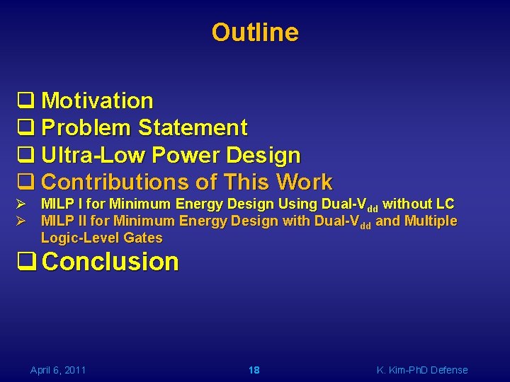
Outline q Motivation q Problem Statement q Ultra-Low Power Design q Contributions of This Work Ø MILP I for Minimum Energy Design Using Dual-Vdd without LC Ø MILP II for Minimum Energy Design with Dual-Vdd and Multiple Logic-Level Gates q Conclusion April 6, 2011 18 K. Kim-Ph. D Defense
![Multiple LogicLevel Gates Delay Multiple LogicLevel NAND 2 11 April 6 2011 Multiple Logic Multiple Logic-Level Gates (Delay) Multiple Logic-Level NAND 2 [11] April 6, 2011 Multiple Logic.](https://slidetodoc.com/presentation_image_h/c590413c59a1a2dc32e90356f4d33d0f/image-19.jpg)
Multiple Logic-Level Gates (Delay) Multiple Logic-Level NAND 2 [11] April 6, 2011 Multiple Logic. Level Gates VVDDH = 300 m. V VVDDL = 230 m. V Norm to INV(FO 4) Vdd = 300 m. V INV 1. 3 NAND 2 2. 3 NAND 3 3. 1 NOR 2 3. 9 DCVS 60. 4 PG 28. 7 SPICE Simulation for PTM 90 nm CMOS At Nominal Vdd = 1. 2 V, Vth, PMOS = -0. 21 V, Vth, NMOS = 0. 29 V Vth, PMOS-HVT = -0. 29 V 19 K. Kim-Ph. D Defense

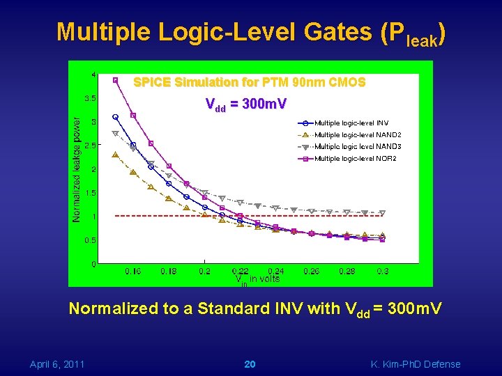
Multiple Logic-Level Gates (Pleak) SPICE Simulation for PTM 90 nm CMOS Vdd = 300 m. V Normalized to a Standard INV with Vdd = 300 m. V April 6, 2011 20 K. Kim-Ph. D Defense

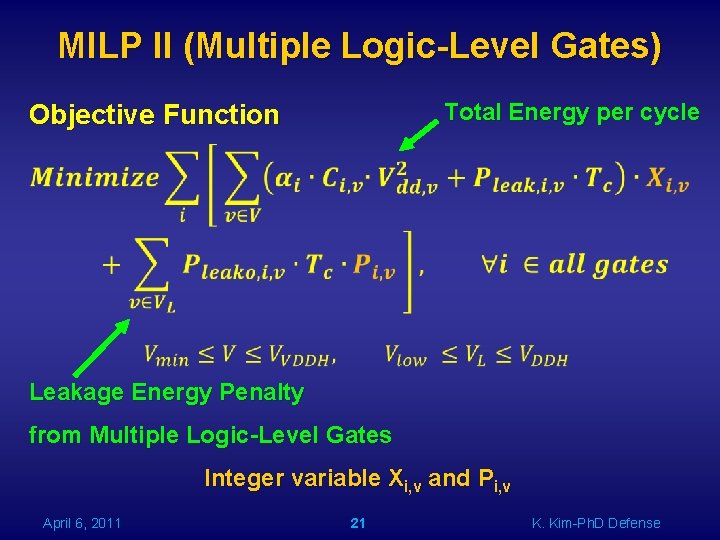
MILP II (Multiple Logic-Level Gates) Total Energy per cycle Objective Function Leakage Energy Penalty from Multiple Logic-Level Gates Integer variable Xi, v and Pi, v April 6, 2011 21 K. Kim-Ph. D Defense

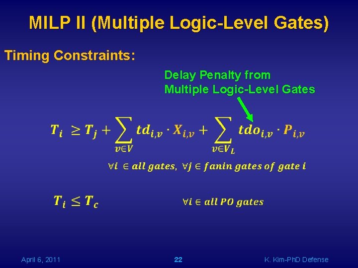
MILP II (Multiple Logic-Level Gates) Timing Constraints: Delay Penalty from Multiple Logic-Level Gates April 6, 2011 22 K. Kim-Ph. D Defense

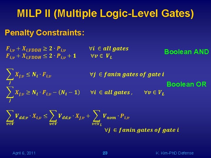
MILP II (Multiple Logic-Level Gates) Penalty Constraints: Boolean AND Boolean OR April 6, 2011 23 K. Kim-Ph. D Defense

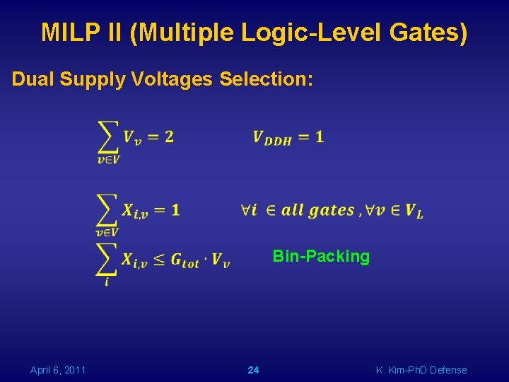
MILP II (Multiple Logic-Level Gates) Dual Supply Voltages Selection: Bin-Packing April 6, 2011 24 K. Kim-Ph. D Defense

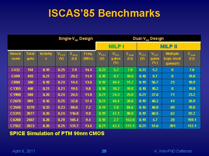
ISCAS’ 85 Benchmarks Single-Vdd Design Dual-Vdd Design MILP II Bench mark Total gate Activity α VDDH (V) Esing. (f. J) Freq. (MHz) VDDL (V) VDDL gates (%) Edual (f. J) VDDL (V) VDDL gates (%) Multiple logic-level gates(#) Edual (f. J) C 432 154 0. 19 0. 25 7. 9 14. 4 0. 23 5. 2 7. 8 0. 23 5. 2 0 7. 8 C 499 493 0. 21 0. 22 20. 2 11. 9 0. 18 9. 7 19. 8 0. 18 9. 7 0 19. 8 C 880 360 0. 18 0. 24 14. 4 13. 6 0. 18 46. 4 11. 2 0. 19 56. 7 23 10. 9 C 1355 469 0. 21 19. 5 9. 8 0. 18 10. 2 19. 0 0. 18 10. 2 0 19. 0 C 1908 584 0. 20 0. 24 26. 5 11. 8 0. 21 24. 3 25. 0 0. 21 27. 6 71 23. 2 C 2670 901 0. 16 0. 25 32. 8 17. 4 0. 21 46. 4 28. 0 0. 19 40. 2 41 26. 9 C 3540 1270 0. 33 0. 23 88. 0 7. 2 0. 14 7. 0 84. 6 0. 16 40. 8 69 70. 8 C 5315 2077 0. 26 0. 24 116. 8 9. 8 0. 19 47. 1 98. 0 0. 19 60. 5 62 92. 2 C 6288 2407 0. 28 0. 29 165. 4 9. 4 0. 18 2. 7 162. 0 0. 19 4. 7 20 159. 1 C 7552 2823 0. 20 0. 25 131. 7 13. 6 0. 21 42. 3 117. 1 0. 21 51. 6 201 112. 1 SPICE Simulation of PTM 90 nm CMOS April 6, 2011 25 K. Kim-Ph. D Defense

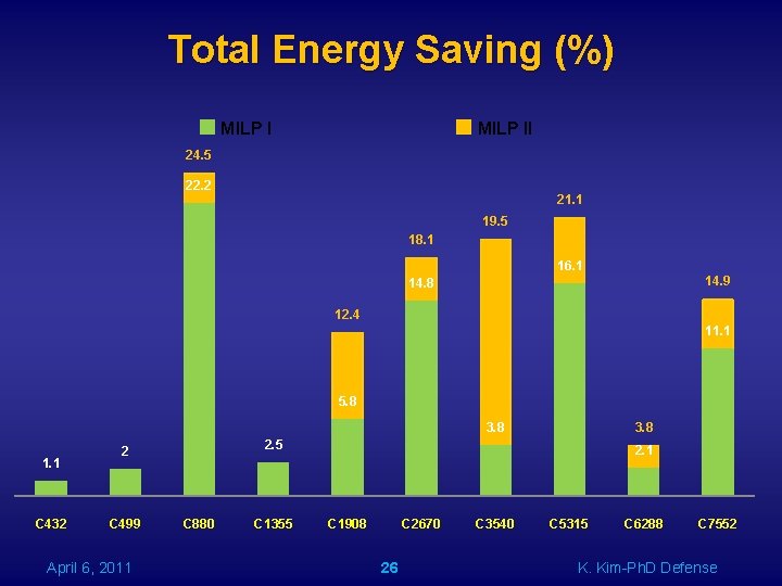
Total Energy Saving (%) MILP II 24. 5 22. 2 21. 1 19. 5 18. 1 16. 1 14. 9 14. 8 12. 4 11. 1 5. 8 3. 8 1. 1 C 432 2. 5 2 C 499 April 6, 2011 3. 8 C 880 C 1355 2. 1 C 1908 C 2670 26 C 3540 C 5315 C 6288 C 7552 K. Kim-Ph. D Defense

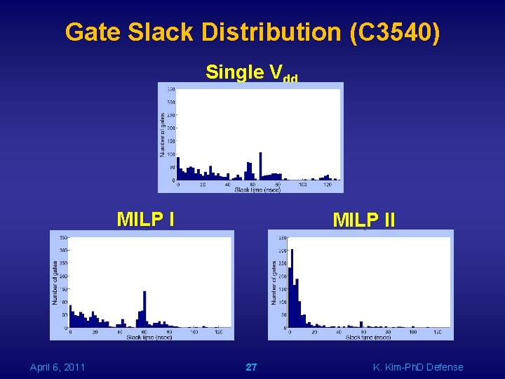
Gate Slack Distribution (C 3540) Single Vdd MILP I April 6, 2011 MILP II 27 K. Kim-Ph. D Defense

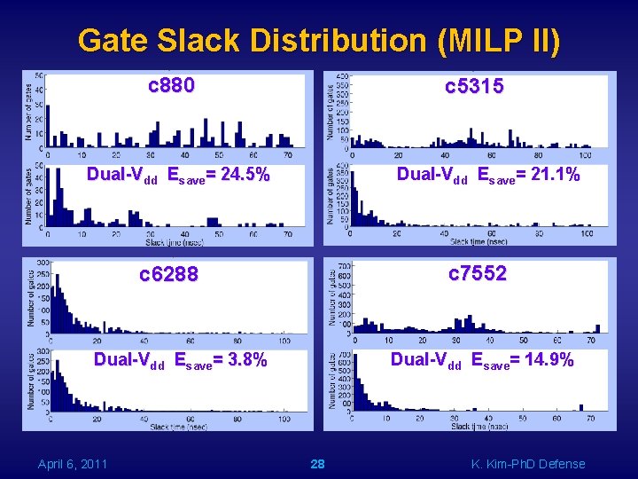
Gate Slack Distribution (MILP II) c 880 c 5315 Dual-Vdd Esave= 21. 1% Dual-Vdd Esave= 24. 5% c 7552 c 6288 Dual-Vdd Esave= 14. 9% Dual-Vdd Esave= 3. 8% April 6, 2011 28 K. Kim-Ph. D Defense

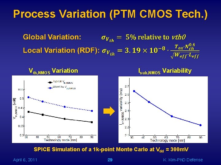
Process Variation (PTM CMOS Tech. ) Vth, NMOS Variation Isub, NMOS Variability SPICE Simulation of a 1 k-point Monte Carlo at Vdd = 300 m. V April 6, 2011 29 K. Kim-Ph. D Defense

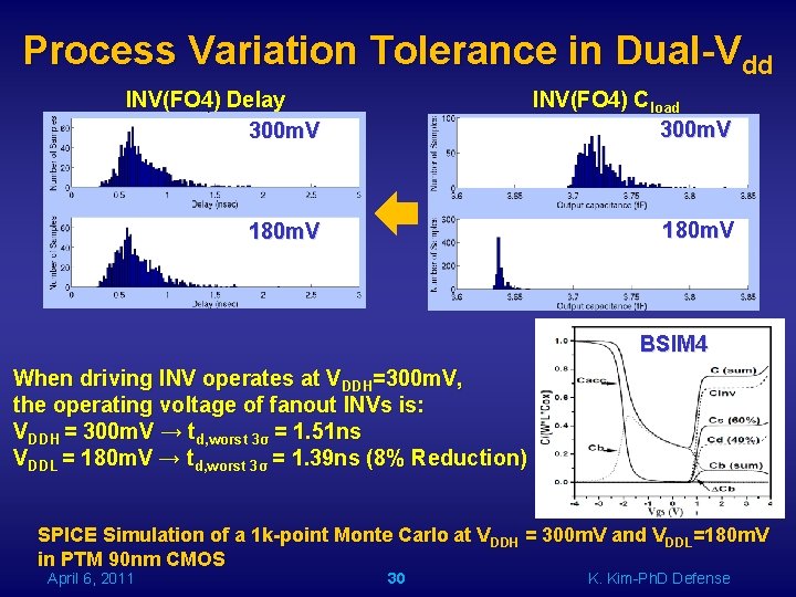
Process Variation Tolerance in Dual-Vdd INV(FO 4) Delay 300 m. V INV(FO 4) Cload 300 m. V 180 m. V BSIM 4 When driving INV operates at VDDH=300 m. V, the operating voltage of fanout INVs is: VDDH = 300 m. V → td, worst 3σ = 1. 51 ns VDDL = 180 m. V → td, worst 3σ = 1. 39 ns (8% Reduction) SPICE Simulation of a 1 k-point Monte Carlo at VDDH = 300 m. V and VDDL=180 m. V in PTM 90 nm CMOS April 6, 2011 30 K. Kim-Ph. D Defense

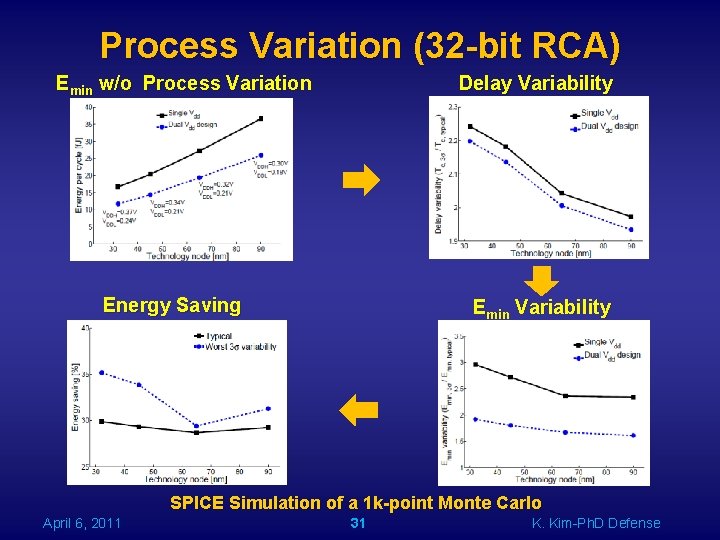
Process Variation (32 -bit RCA) Delay Variability Emin w/o Process Variation Energy Saving Emin Variability SPICE Simulation of a 1 k-point Monte Carlo April 6, 2011 31 K. Kim-Ph. D Defense

Outline q Motivation q Problem Statement q Ultra-Low Power Design q Contributions of This Work Ø MILP I for Minimum Energy Design Using Dual-Vdd without LC Ø MILP II for Minimum Energy Design with Dual-Vdd and Multiple Logic-Level Gates Ø Linear-Time Algorithm for Dual-Vdd Using Gate Slack q Conclusion April 6, 2011 32 K. Kim-Ph. D Defense

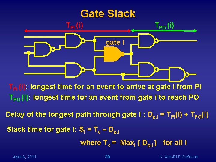
Gate Slack TPI (i) TPO (i) gate i TPI (i): longest time for an event to arrive at gate i from PI TPO (i): longest time for an event from gate i to reach PO Delay of the longest path through gate i : Dp, i = TPI(i) + TPO(i) Slack time for gate i: Si = Tc – Dp, i where T c = Maxi { Dp, i } for all i April 6, 2011 33 K. Kim-Ph. D Defense

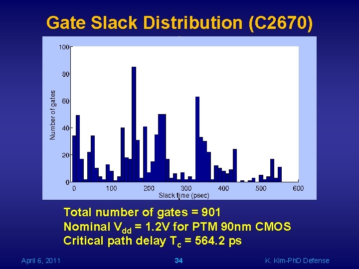
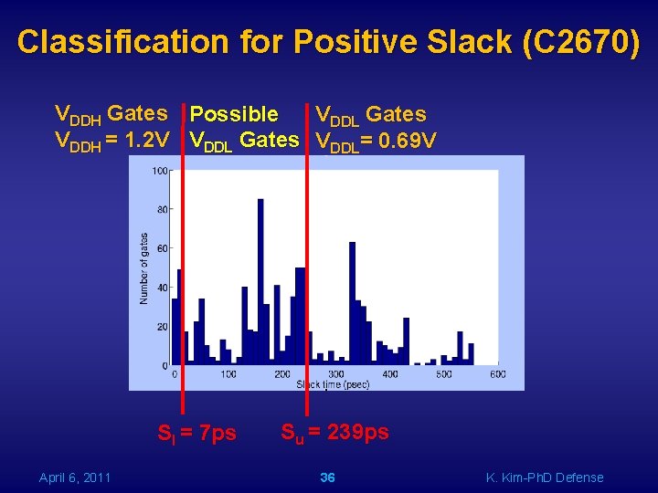
Gate Slack Distribution (C 2670) Total number of gates = 901 Nominal Vdd = 1. 2 V for PTM 90 nm CMOS Critical path delay Tc = 564. 2 ps April 6, 2011 34 K. Kim-Ph. D Defense

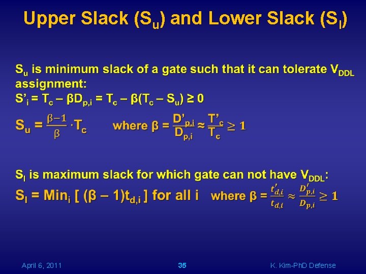
Upper Slack (Su) and Lower Slack (Sl) April 6, 2011 35 K. Kim-Ph. D Defense

Classification for Positive Slack (C 2670) VDDH Gates Possible VDDL Gates VDDH = 1. 2 V VDDL Gates VDDL= 0. 69 V Sl = 7 ps April 6, 2011 Su = 239 ps 36 K. Kim-Ph. D Defense

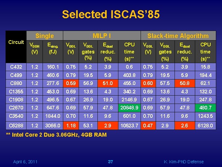
Selected ISCAS’ 85 Circuit Single MILP I Slack-time Algorithm VDDH (V) Esing. (f. J) VDDL (V) VDDL gates (%) Edual reduc. (%) CPU time (s)** C 432 1. 2 160. 1 0. 75 5. 2 3. 9 0. 6 0. 75 5. 2 3. 9 15. 8 C 499 1. 2 460. 6 0. 79 19. 5 5. 9 403. 8 0. 79 19. 5 5. 9 194. 4 C 880 1. 2 277. 6 0. 59 56. 9 51. 0 455. 0 0. 60 57. 5 50. 8 62. 1 C 1355 1. 2 453. 0 0. 69 13. 6 4. 3 340. 2 0. 69 13. 6 4. 3 132. 0 C 1908 1. 2 496. 5 0. 67 26. 9 19. 0 2146. 9 0. 67 26. 9 19. 0 247. 8 C 2670 1. 2 647. 6 0. 69 57. 9 47. 8 20848. 9 0. 69 57. 9 47. 8 480. 7 C 3540 1. 2 1844. 0 0. 70 11. 6 9. 6 1243. 5 C 6288 1. 2 3066. 0 1. 18 53. 1 2. 9 10523. 7 0. 47 2. 9 2. 6 6128. 0 601. 0 ** Intel Core 2 Duo 3. 06 GHz, 4 GB RAM April 6, 2011 37 K. Kim-Ph. D Defense

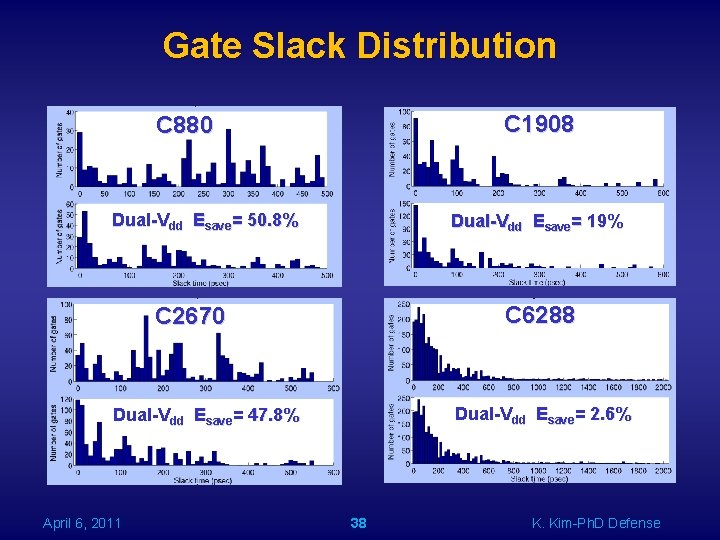
Gate Slack Distribution C 1908 C 880 Dual-Vdd Esave= 50. 8% Dual-Vdd Esave= 19% C 6288 C 2670 Dual-Vdd Esave= 2. 6% Dual-Vdd Esave= 47. 8% April 6, 2011 38 K. Kim-Ph. D Defense

Outline q Motivation q Problem Statement q Ultra-Low Power Design q Contributions of This Work Ø MILP I for Minimum Energy Design Using Dual-Vdd without LC Ø MILP II for Minimum Energy Design with Dual-Vdd and Multiple Logic-Level Gates Ø Linear-Time Algorithm for Dual-Vdd Using Gate Slack q Conclusion April 6, 2011 39 K. Kim-Ph. D Defense

Conclusion q Dual Vdd design is valid for energy reduction below the minimum energy point in a single Vdd as well as for substantial speed-up within tight energy budget of a bulk CMOS subthreshold circuit. § Conventional level converters are not usable due to huge delay penalty in subthreshold regime. § MILP I finds the optimal Vdd and its assignment for minimum energy design without using LC. § MILP II improves the energy saving using multiple logic-level gates to eliminate topological constraints for dual-Vdd design. q Proposed algorithm for dual-Vdd using linear-time gate slack analysis can reduce the time complexity, ~O(n), for n gates in the circuit. § Runtime of MILP is too expensive and heuristic algorithms still have polynomial time complexity O(n 2). § Gate slack analysis unconditionally classifies all gates into VDDL, possible VDDL, and VDDH gates. § The methodology of slack classification can be applied to other power optimization disciplines, such as dual-Vth. April 6, 2011 40 K. Kim-Ph. D Defense

List of Publications § K. Kim and V. D. Agrawal, “Minimum Energy CMOS Design with Dual Subthreshold Supply and Multiple Logic-Level Gates”, in IEEE Journal on Emerging and Selected Topics in Circuits and Systems (Submitted) § K. Kim and V. D. Agrawal, “Minimum Energy CMOS Design with Dual Subthreshold Supply and Multiple Logic-Level Gates”, in Proc. 12 th International Symposium on Quality Electronic Design, Mar. 2011, pp. 689 -694. § K. Kim and V. D. Agrawal, “Dual Voltage Design for Minimum Energy Using Gate Slack”, in Proc. IEEE International Conference on Industrial Technology, Mar. 2011, pp. 405 -410. § K. Kim and V. D. Agrawal, “True Minimum Energy Design Using Dual Below Threshold Supply Voltages”, in Proceedings of 24 th International Conference on VLSI Design, Jan. 2011, paper C 2 -3. (Selected for a special issue of JOLPE). April 6, 2011 41 K. Kim-Ph. D Defense
![References 1 A Wang B H Calhoun and A P Chandrakasan SubThreshold Design for References [1] A. Wang, B. H. Calhoun, and A. P. Chandrakasan, Sub-Threshold Design for](https://slidetodoc.com/presentation_image_h/c590413c59a1a2dc32e90356f4d33d0f/image-42.jpg)
References [1] A. Wang, B. H. Calhoun, and A. P. Chandrakasan, Sub-Threshold Design for Ultra Low-Power Systems. Springer, 2006 A. Wang, B. H. Calhoun, and A. P. Chandrakasan, Sub-Threshold Systems. Springer, 2006. . [2] D. Bol, D. Flandre, and J. -D. Legat, “Technology Flavor Selection and Adaptive Techniques for Timing-Constrained 45 nm Subthreshold Circuits, ” in Proceedings of the 14 th ACM/IEEE International Symposium on Low Power Electronics and Design, Subthreshold Circuits, ” in Proceedings Design, 2009, pp. 21– 26. [3] Solar C Cells, ” in Proc. [3] G. Chen et al, “Millimeter-Scale Nearly Perpetual Sensor System with Stacked Battery and Solar ells, ” in Proc. ISSCC 2010, pp. 288– 289. [4] Kim, C. H. Roy, K K. , "Ultra-low-power DLMS adaptive filter for hearing aid applications, " IEEE Transactions Kim, C. H. -II, Soeleman, H. and Roy, , "Ultra-low-power DLMS adaptive filter for hearing aid applications, " IEEE on Very Large Scale Integration (VLSI) Systems , vol. 11, no. 6, pp. 1058 - 1067, Dec. 2003. [5] A. Wang and A. Chandrakasan, “A 180 m. V FFT Processor Using Subthreshold Circuit Techniques, ” in IEEE International Solid-State Circuits Conference Digest of Technical Papers, 2004, pp. 292– 529. [6] B. Zhai, et al, “A 2. 60 p. J/Inst Subthreshold Sensor Processor for Optimal Energy Efficiency”, Proc. Symposium on VLSI. Zhai, et al, “A 2. 60 p. J/Inst Subthreshold Sensor Processor for Optimal Energy Efficiency”, circuits, 2006 [7] J. Kwong, et al, “A 65 nm Sub-Vt Microcontroller with Integrated SRAM and Switched-Capacitor DC-DC Converter”, Proc. . Kwong, et al, “A 65 nm Sub-Vt Microcontroller with Integrated SRAM and Switched-Capacitor DC-DC Converter”, ISSCC, 2008 [8] M. Seok, D. Sylvester, and D. Blaauw, “Optimal Technology Selection for Minimizing Energy and Variability in Low Voltage Applications, ” in Proc. of International Symp. Low Power Electronics and Design, 2008, pp. 9– 14 Applications, ” in Proc. Design, 2008, pp. 9– 14. . [9] K. Usami and M. Horowitz, “Clustered Voltage Scaling Technique for Low-Power Design, ” in Proc. International Symposium. Usami and M. Horowitz, “Clustered Voltage Scaling Technique for Low-Power Design, ” in on Low Power Design, 1995, pp. 3– 8. . Design, 1995, pp. 3– 8 [10] K. Usami, M. Igarashi, F. Minami, T. Ishikawa, M. Kanzawa, M. Ichida , and K. Nogami, “Automated Low-Power Technique . Usami, M. Igarashi, F. Minami, T. Ishikawa, M. Kanzawa, M. Ichida, Exploiting Multiple Supply Voltages Applied to a Media Processor, ” IEEE Journal of Solid-State Circuits, vol. 33, no. 3, pp. . Exploiting Multiple Supply Voltages Applied Circuits, vol. 33, no. 3, pp 463 -472, 1998. . [11] A. U. Diril, Y. S. Dhillon, A. Chatterjee, and A. D. Singh, “Level-Shifter Free Design of Low Power Dual Supply Voltage CMOS . U. Diril, Y. S. Dhillon, A. Chatterjee, and A. D. Singh, “Level-Shifter Free Design of Circuits Using Dual Threshold Voltages, ” IEEE Trans. on Circuits Using Dual Threshold Voltages, ” on VLSI Systems, vol. 13, no. 9, pp. 1103– 1107, Sept. 2005. . April 6, 2011 42 K. Kim-Ph. D Defense

THANK YOU!! & QUESTIONS? April 6, 2011 43 K. Kim-Ph. D Defense