Ultimate MIMO i PHC Ultimate Chip Floor Plan

- Slides: 6

Ultimate MIMO

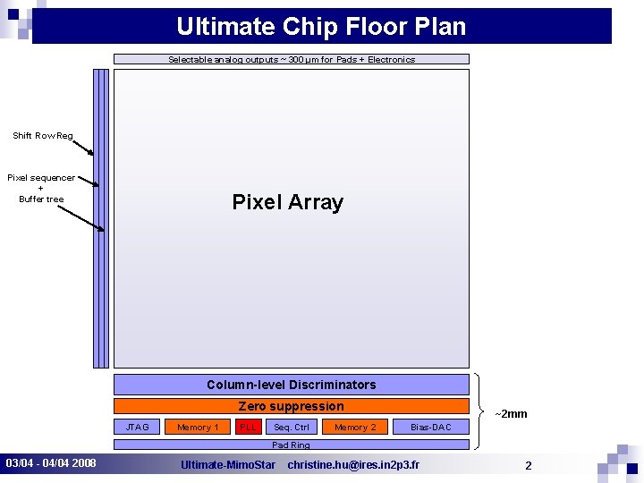
i. PHC Ultimate Chip Floor Plan Selectable analog outputs ~ 300 µm for Pads + Electronics Shift Row Reg Pixel sequencer + Buffer tree Pixel Array Column-level Discriminators Zero suppression JTAG Memory 1 PLL Seq. Ctrl Memory 2 ~2 mm Bias-DAC Pad Ring 03/04 - 04/04 2008 Ultimate-Mimo. Star christine. hu@ires. in 2 p 3. fr 2

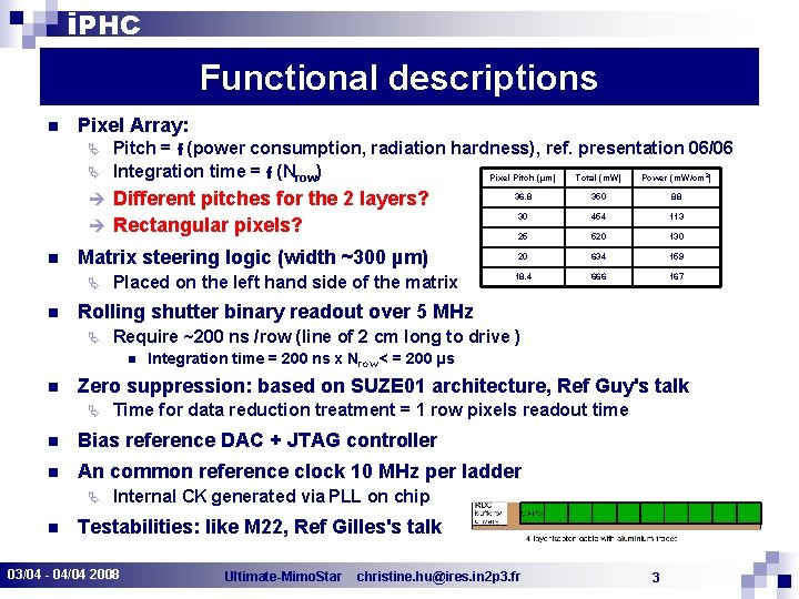
i. PHC Functional descriptions n Pixel Array: Pitch = f (power consumption, radiation hardness), ref. presentation 06/06 Ä Integration time = f (Nrow) Pixel Pitch (µm) Total (m. W) Power (m. W/cm ) Ä 2 Different pitches for the 2 layers? è Rectangular pixels? è n Matrix steering logic (width ~300 µm) Ä n Placed on the left hand side of the matrix 350 88 30 454 113 25 520 130 20 634 159 18. 4 666 167 Rolling shutter binary readout over 5 MHz Ä Require ~200 ns /row (line of 2 cm long to drive ) n n 36. 8 Integration time = 200 ns x Nrow < = 200 µs Zero suppression: based on SUZE 01 architecture, Ref Guy's talk Ä Time for data reduction treatment = 1 row pixels readout time n Bias reference DAC + JTAG controller n An common reference clock 10 MHz per ladder Ä n Internal CK generated via PLL on chip Testabilities: like M 22, Ref Gilles's talk 03/04 - 04/04 2008 Ultimate-Mimo. Star christine. hu@ires. in 2 p 3. fr 3

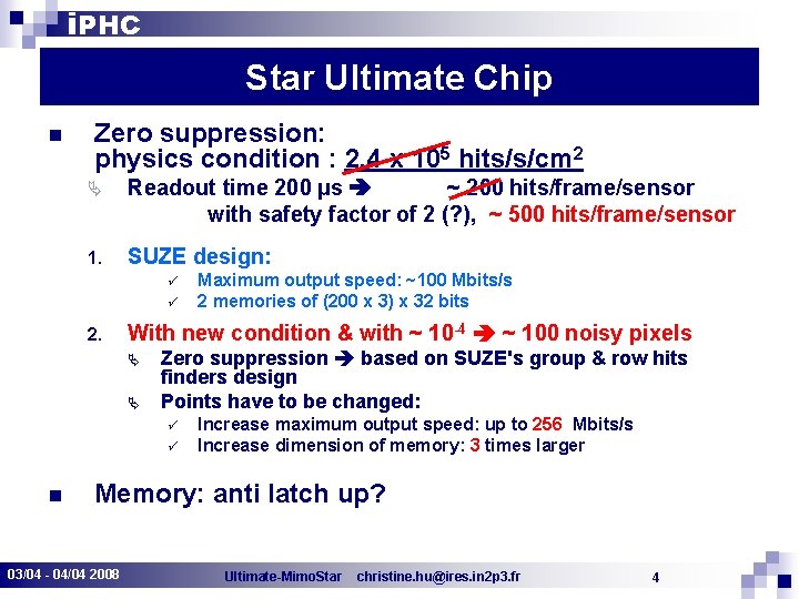
i. PHC Star Ultimate Chip n Zero suppression: physics condition : 2, 4 x 10⁵ hits/s/cm 2 Ä Readout time 200 µs ~ 200 hits/frame/sensor with safety factor of 2 (? ), ~ 500 hits/frame/sensor 1. SUZE design: ü ü 2. With new condition & with ~ 10 -4 ~ 100 noisy pixels Ä Ä Zero suppression based on SUZE's group & row hits finders design Points have to be changed: ü ü n Maximum output speed: ~100 Mbits/s 2 memories of (200 x 3) x 32 bits Increase maximum output speed: up to 256 Mbits/s Increase dimension of memory: 3 times larger Memory: anti latch up? 03/04 - 04/04 2008 Ultimate-Mimo. Star christine. hu@ires. in 2 p 3. fr 4

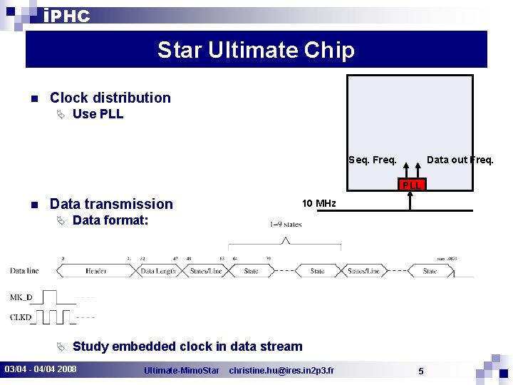
i. PHC Star Ultimate Chip n Clock distribution Ä Use PLL Seq. Freq. Data out Freq. PLL n Data transmission 10 MHz Ä Data format: Ä Study embedded clock in data stream 03/04 - 04/04 2008 Ultimate-Mimo. Star christine. hu@ires. in 2 p 3. fr 5

i. PHC LBNL Mechanical Requirements n n 3 or 4 fiducial marks/chip for optical survey All bonding pads located along 1 side of chip Ä n Except analog test pads Two bonding pads per I/O (if possible) of the chip to facilitate probe testing 03/04 - 04/04 2008 Ultimate-Mimo. Star christine. hu@ires. in 2 p 3. fr 6