UCLA Architecture and Synthesis for PowerEfficient FPGAs Jason

![Why? FPGA is Known to be Power Inefficient! Source: [Zuchowski, et al, ICCAD 02] Why? FPGA is Known to be Power Inefficient! Source: [Zuchowski, et al, ICCAD 02]](https://slidetodoc.com/presentation_image_h/0636c15483af2a29c3e5a949e4766a17/image-3.jpg)
- Slides: 31

UCLA Architecture and Synthesis for Power-Efficient FPGAs Jason Cong University of California, Los Angeles cong@cs. ucla. edu Joint work with Deming Chen, Lei He, Fei Li, Yan Lin Partially supported by NSF Grants CCR-0096383, and CCR-0306682, and Altera under the California MICRO program

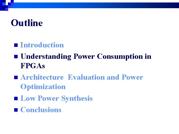
Outline Introduction n Understanding Power Consumption in FPGAs n Architecture Evaluation and Power Optimization n Low Power Synthesis n Conclusions n
![Why FPGA is Known to be Power Inefficient Source Zuchowski et al ICCAD 02 Why? FPGA is Known to be Power Inefficient! Source: [Zuchowski, et al, ICCAD 02]](https://slidetodoc.com/presentation_image_h/0636c15483af2a29c3e5a949e4766a17/image-3.jpg)
Why? FPGA is Known to be Power Inefficient! Source: [Zuchowski, et al, ICCAD 02] n n FPGA consumes 50 -100 X more power Why do we care about power optimization for FPGAs ? !

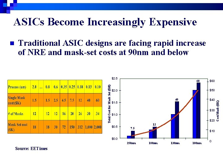
ASICs Become Increasingly Expensive Traditional ASIC designs are facing rapid increase of NRE and mask-set costs at 90 nm and below $2. 5 60 $50 $2. 0 40 $1. 5 $40 $30 $1. 0 $20 $0. 5 12 7. 5 $10 $0. 0 250 nm Source: EETimes $60 180 nm 130 nm 100 nm 0 Cost/Mask ($K) Total Cost for Mask Set ($M) n

FPGA Advantages n n Short TAT (total turnaround time) No or very low NRE

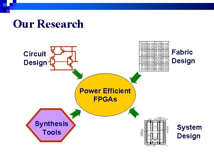
Our Research Fabric Design Circuit Design Power Efficient FPGAs Synthesis Tools System Design

Outline Introduction n Understanding Power Consumption in FPGAs n Architecture Evaluation and Power Optimization n Low Power Synthesis n Conclusions n

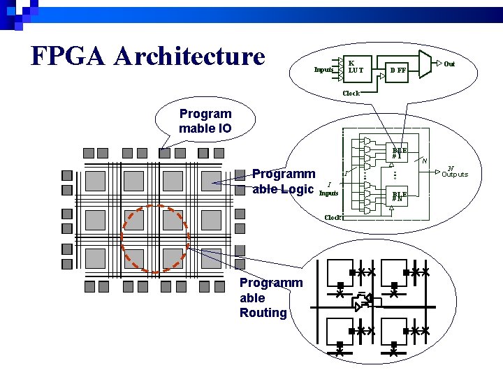
FPGA Architecture K LUT Inputs Out D FF Clock Program mable IO BLE #1 Programm able Logic I I Inputs Clock Programm able Routing BLE #N N N Outputs

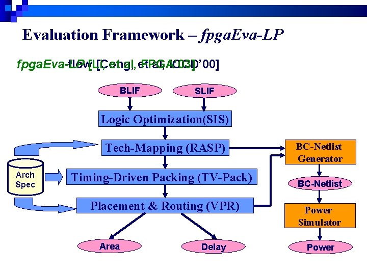
Evaluation Framework – fpga. Eva-LP fpga. Eva flow[Li, fpga. Eva-LP [Cong, et al, et FPGA’ 03] al, ICCD’ 00] BLIF SLIF Logic Optimization(SIS) Tech-Mapping (RASP) Arch Spec Timing-Driven Packing (TV-Pack) Placement & Routing (VPR) Area Delay BC-Netlist Generator BC-Netlist Power Simulator Power

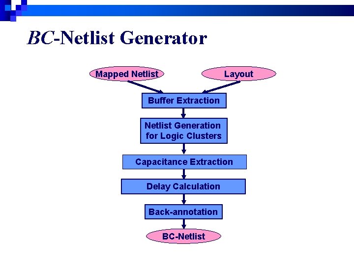
BC-Netlist Generator Layout Mapped Netlist Buffer Extraction Netlist Generation for Logic Clusters Capacitance Extraction Delay Calculation Back-annotation BC-Netlist

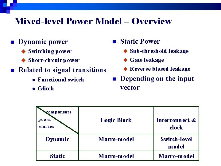
Mixed-level Power Model – Overview n Dynamic power n Sub-threshold leakage u Gate leakage u Reverse biased leakage Switching power u Short-circuit power u u n Related to signal transitions l l Functional switch Glitch components power sources Static Power n Depending on the input vector Logic Block Interconnect & clock Dynamic Macro-model Switch-level model Static Macro-model

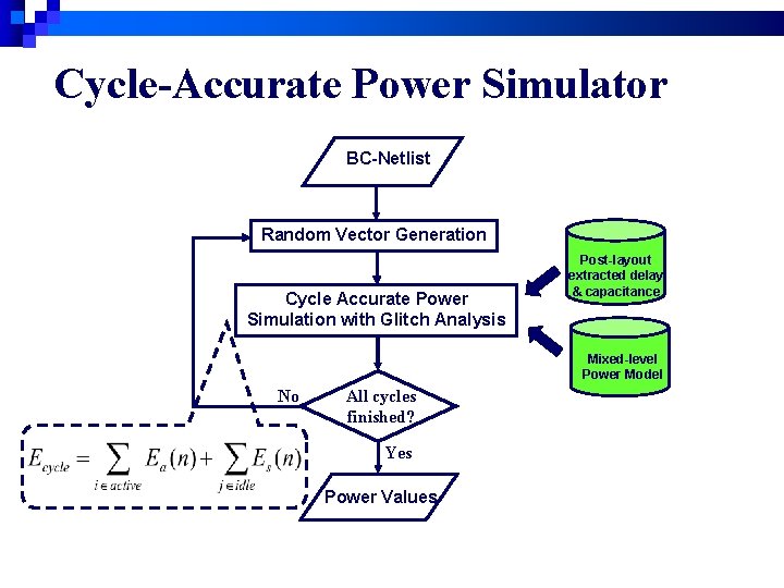
Cycle-Accurate Power Simulator BC-Netlist Random Vector Generation Cycle Accurate Power Simulation with Glitch Analysis Post-layout extracted delay & capacitance Mixed-level Power Model No All cycles finished? Yes Power Values

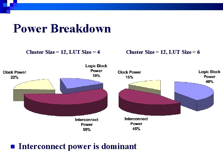
Power Breakdown Cluster Size = 12, LUT Size = 4 n Cluster Size = 12, LUT Size = 6 Interconnect power is dominant

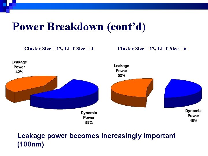
Power Breakdown (cont’d) Cluster Size = 12, LUT Size = 4 q Cluster Size = 12, LUT Size = 6 Leakage power becomes increasingly important (100 nm)

Outline n n n Introduction Understanding Power Consumption in FPGAs Architecture Evaluation and Power Optimization u Architecture Parameter Selection u Dual-Vdd/Dual-Vt FPGA Architecture n n Low Power Synthesis with Dual-Vdd Conclusion

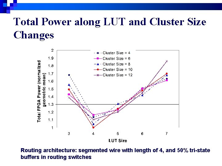
Total Power along LUT and Cluster Size Changes Routing architecture: segmented wire with length of 4, and 50% tri-state buffers in routing switches

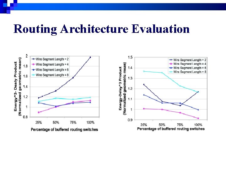
Routing Architecture Evaluation

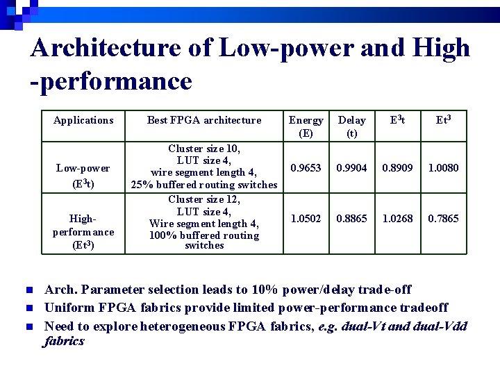
Architecture of Low-power and High -performance Applications Low-power (E 3 t) Highperformance (Et 3) n n n Best FPGA architecture Cluster size 10, LUT size 4, wire segment length 4, 25% buffered routing switches Cluster size 12, LUT size 4, Wire segment length 4, 100% buffered routing switches Energy (E) Delay (t) E 3 t Et 3 0. 9653 0. 9904 0. 8909 1. 0080 1. 0502 0. 8865 1. 0268 0. 7865 Arch. Parameter selection leads to 10% power/delay trade-off Uniform FPGA fabrics provide limited power-performance tradeoff Need to explore heterogeneous FPGA fabrics, e. g. dual-Vt and dual-Vdd fabrics

Outline n n n Introduction Understanding Power Consumption in FPGAs Architecture Evaluation and Power Optimization u Architecture Parameter Selection u Dual-Vdd/Dual-Vt FPGA Architecture [Li, et al, FPGA’ 04] n n Low Power Synthesis with Dual-Vdd Conclusion

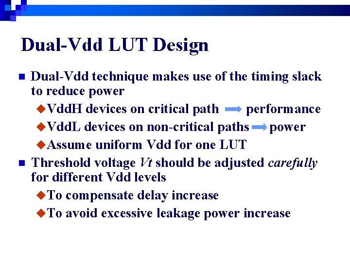
Dual-Vdd LUT Design n n Dual-Vdd technique makes use of the timing slack to reduce power u. Vdd. H devices on critical path performance u. Vdd. L devices on non-critical paths power u. Assume uniform Vdd for one LUT Threshold voltage Vt should be adjusted carefully for different Vdd levels u. To compensate delay increase u. To avoid excessive leakage power increase

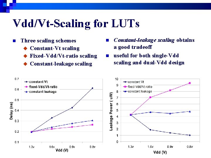
Vdd/Vt-Scaling for LUTs n Three scaling schemes u Constant-Vt scaling u Fixed-Vdd/Vt-ratio scaling u Constant-leakage scaling n n Constant-leakage scaling obtains a good tradeoff useful for both single-Vdd scaling and dual-Vdd design

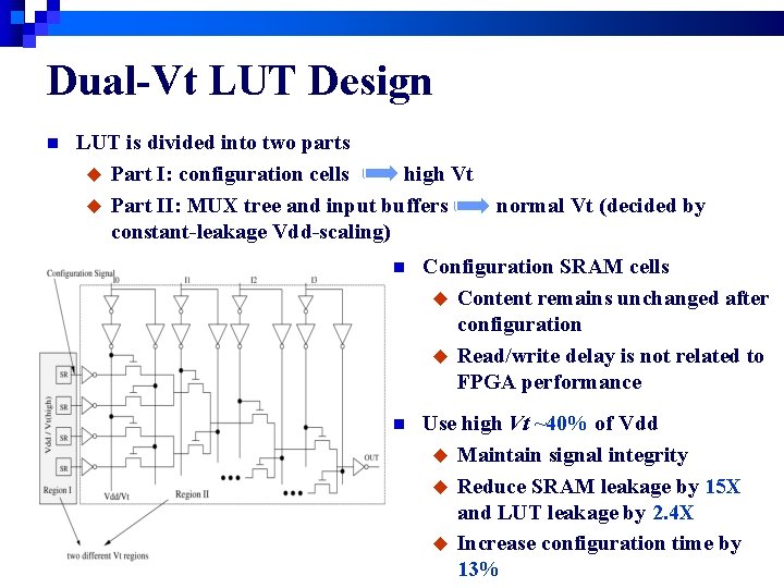
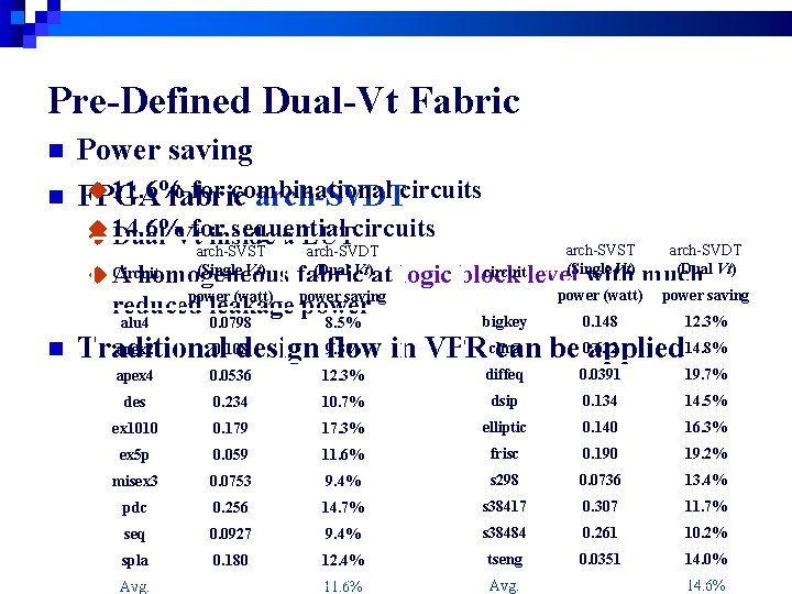
Dual-Vt LUT Design n LUT is divided into two parts u Part I: configuration cells high Vt u Part II: MUX tree and input buffers constant-leakage Vdd-scaling) normal Vt (decided by n Configuration SRAM cells u Content remains unchanged after configuration u Read/write delay is not related to FPGA performance n Use high Vt ~40% of Vdd u Maintain signal integrity u Reduce SRAM leakage by 15 X and LUT leakage by 2. 4 X u Increase configuration time by 13%

Pre-Defined Dual-Vt Fabric n Power saving u 11. 6% for combinational n FPGA fabric arch-SVDTcircuits u sequential u 14. 6% Dual-Vtfor inside a LUTcircuits arch-SVST (Single Vt) arch-SVDT (Dual Vt) alu 4 0. 0798 8. 5% apex 4 0. 0536 12. 3% diffeq 0. 0391 19. 7% des 0. 234 10. 7% dsip 0. 134 14. 5% ex 1010 0. 179 17. 3% elliptic 0. 140 16. 3% ex 5 p 0. 059 11. 6% frisc 0. 190 19. 2% misex 3 0. 0753 9. 4% s 298 0. 0736 13. 4% pdc 0. 256 14. 7% s 38417 0. 307 11. 7% seq 0. 0927 9. 4% s 38484 0. 261 10. 2% u Circuit A homogeneous circuit level with much fabric at logic block power (watt) power saving power (watt) saving reduced leakage power bigkey 0. 148 12. 3% n apex 2 0. 108 Traditional design 9. 3% flow in VPR clma can be 0. 632 applied 14. 8% spla 0. 180 12. 4% Table 1 Combinational circuits Avg. 11. 6% tseng 0. 0351 14. 0% Table 2 Sequential circuits Avg. 14. 6%

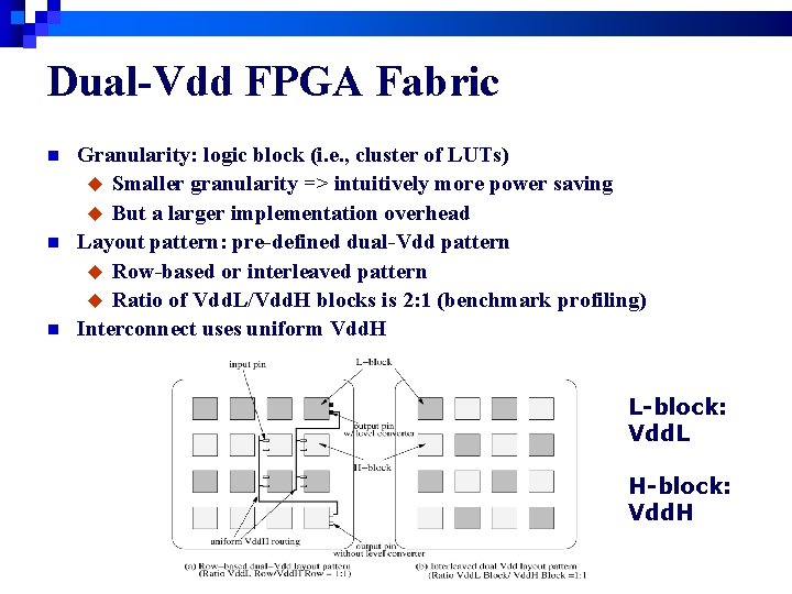
Dual-Vdd FPGA Fabric n n n Granularity: logic block (i. e. , cluster of LUTs) u Smaller granularity => intuitively more power saving u But a larger implementation overhead Layout pattern: pre-defined dual-Vdd pattern u Row-based or interleaved pattern u Ratio of Vdd. L/Vdd. H blocks is 2: 1 (benchmark profiling) Interconnect uses uniform Vdd. H L-block: Vdd. L H-block: Vdd. H

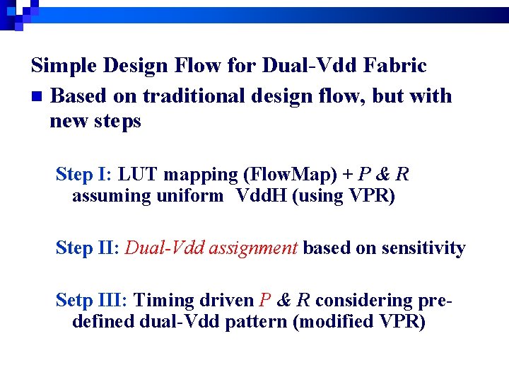
Simple Design Flow for Dual-Vdd Fabric n Based on traditional design flow, but with new steps Step I: LUT mapping (Flow. Map) + P & R assuming uniform Vdd. H (using VPR) Step II: Dual-Vdd assignment based on sensitivity Setp III: Timing driven P & R considering predefined dual-Vdd pattern (modified VPR)

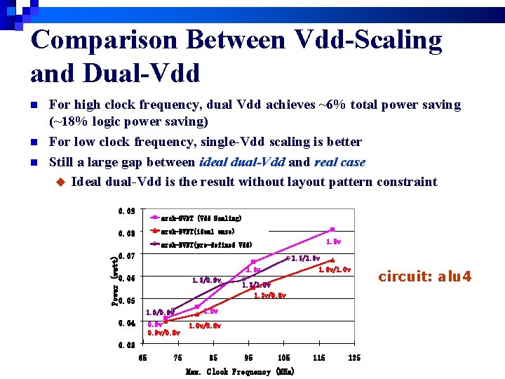
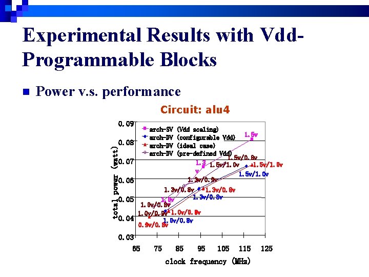
Comparison Between Vdd-Scaling and Dual-Vdd n n For high clock frequency, dual Vdd achieves ~6% total power saving (~18% logic power saving) For low clock frequency, single-Vdd scaling is better Still a large gap between ideal dual-Vdd and real case u Ideal dual-Vdd is the result without layout pattern constraint 0. 09 arch-SVDT (Vdd Scaling) arch-DVDT(ideal case) 0. 08 1. 5 v arch-DVDT(pre-defined Vdd) Power (watt) n 0. 07 1. 5/1. 0 v 1. 5 v/1. 0 v 1. 3 v 0. 06 1. 3/0. 9 v 1. 3/1. 0 v 1. 3 v/0. 8 v 0. 05 1. 0/0. 9 v 0. 04 0. 9 v/0. 8 v 1. 0 v/0. 8 v 0. 03 65 75 85 95 105 Max. Clock Frequency (MHz) 115 125 circuit: alu 4

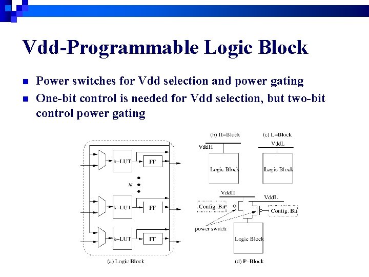
Vdd-Programmable Logic Block n n Power switches for Vdd selection and power gating One-bit control is needed for Vdd selection, but two-bit control power gating

Experimental Results with Vdd. Programmable Blocks Power v. s. performance Circuit: alu 4 0. 09 0. 08 total power (watt) n 0. 07 0. 06 0. 05 0. 04 (Vdd scaling) (configurable Vdd) 1. 5 v (ideal case) (pre-defined Vdd) 1. 5 v/0. 8 v 1. 3 1. 5 v/1. 0 v v 1. 5 v/1. 0 v 1. 3 v/0. 9 v 1. 3 v/0. 8 v 1. 0 v/0. 9 v 1. 0 v/0. 8 v 0. 9 v/0. 8 v 0. 03 65 arch-SV arch-DV 75 85 95 105 115 clock frequency (MHz) 125

Outline Introduction n Understanding Power Consumption in FPGAs n Architecture Evaluation and Power Optimization n Low Power Synthesis n Conclusions n

Low Power Synthesis for Dual Vdd FPGAs FPGA architecture with dual-Vdds adds new layout constraints for synthesis tools n Novel synthesis tools are required to support the architecture n u. Technology mapping [Chen, et al, FPGA’ 04] u. Circuit clustering [Chen, et al, ISLPED’ 04]

Conclusions n FPGA power consumption Majority on programmable interconnects u Leakage is significant u n FPGA architecture optimization for power Architecture parameter tuning has a limited impact u Using high Vt for configuration SRAM cells is helpful u Using programmable dual Vdd for logic blocks is helpful u n Power-efficient FPGA architectures introduce interesting CAD problems Dual-Vdd mapping u Dual-Vdd clustering Up to 20% power saving reported using these algorithms u