
UCC 28740 Feedback Loop Compensation Design 1 Flyback
UCC 28740 Feedback Loop Compensation Design 1

Flyback Regulator Schematic Diagram using UCC 28740 with Opto-coupled Feedback TL 431 2
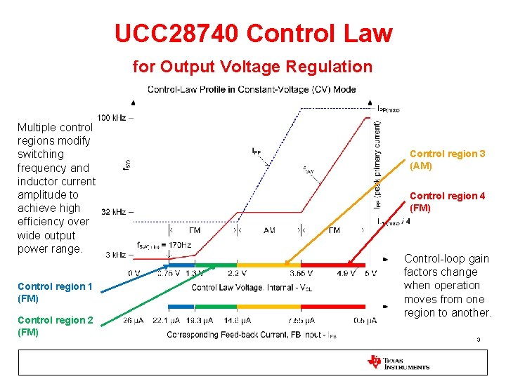
UCC 28740 Control Law for Output Voltage Regulation Multiple control regions modify switching frequency and inductor current amplitude to achieve high efficiency over wide output power range. Control region 1 (FM) Control region 2 (FM) Control region 3 (AM) Control region 4 (FM) Control-loop gain factors change when operation moves from one region to another. 3

Voltage Feedback Loop Block Diagram in FM Regions of Control Law VIN VCSn IOUT + i. O GPn n = 1, 2, or 4, depending on FM region of operation f. SW KFMn VOUT + v. O ZL(s) v. CL GFB 2 i. FB GFB 1 i. E GOPTO(s) v. O i. D G 431(s) Control-Loop Gain: AV = G 431(s) · GOPTO(S) · GFB 1 · GFB 2 · KFMn · GPn · ZL(s) 4

Voltage Feedback Loop Block Diagram in AM Region of Control Law VIN FAM IOUT + i. O GP 3 VOUT + v. O ZL(s) v. CS KAM v. O v. CL GFB 2 i. FB GFB 1 i. E GOPTO(s) i. D G 431(s) Control-Loop Gain: AV = G 431(s) · GOPTO(S) · GFB 1 · GFB 2 · KAM 3 · GP 3 · ZL(s) 5

Gain Blocks Defined – G 431(s) Output voltage sense to opto-coupler diode current gain: i. D TL 431 6
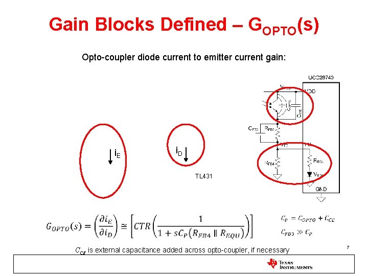
Gain Blocks Defined – GOPTO(s) Opto-coupler diode current to emitter current gain: i. E i. D TL 431 CCE is external capacitance added across opto-coupler, if necessary 7
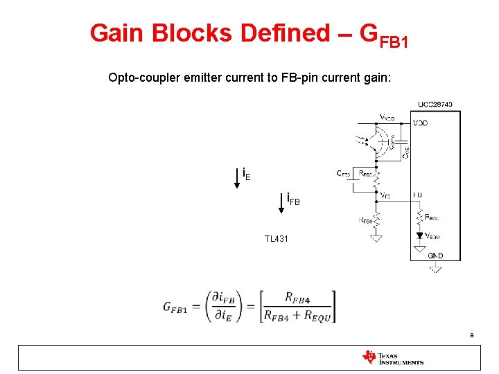
Gain Blocks Defined – GFB 1 Opto-coupler emitter current to FB-pin current gain: i. E i. FB TL 431 8
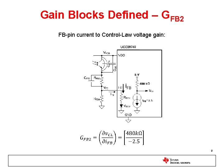
Gain Blocks Defined – GFB 2 FB-pin current to Control-Law voltage gain: i. FBi FB 9
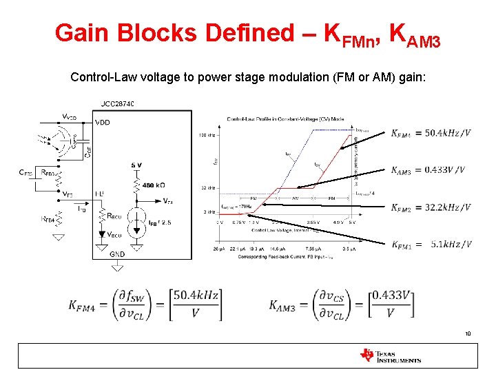
Gain Blocks Defined – KFMn, KAM 3 Control-Law voltage to power stage modulation (FM or AM) gain: 10
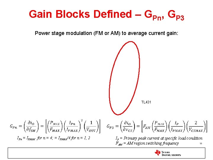
Gain Blocks Defined – GPn, GP 3 Power stage modulation (FM or AM) to average current gain: TL 431 IPn = IPMAX for n = 4; = IPMAX/4 for n = 1, 2 IP = Primary peak current at specific load condition 11 FAM = AM region switching frequency
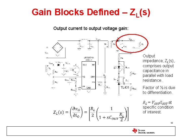
Gain Blocks Defined – ZL(s) Output current to output voltage gain: Output impedance, ZL(s), comprises output capacitance in parallel with load resistance. TL 431 Factor of ½ is due to differentiation. RL = VOUT/IOUT at specific condition of interest. 12
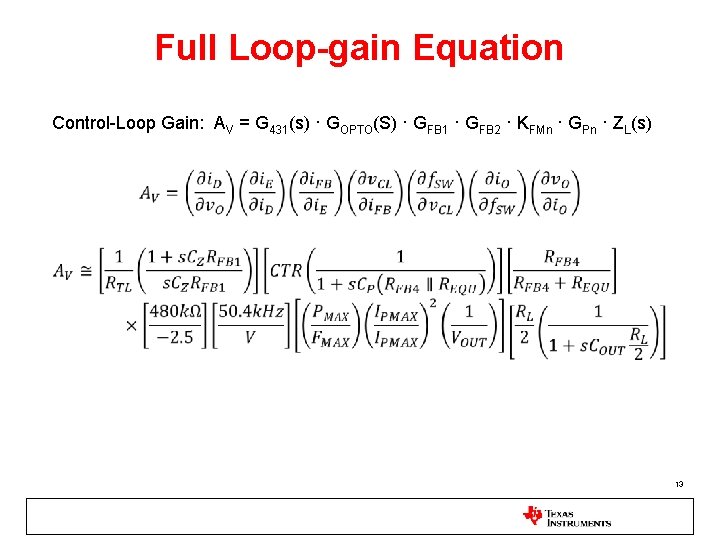
Full Loop-gain Equation Control-Loop Gain: AV = G 431(s) · GOPTO(S) · GFB 1 · GFB 2 · KFMn · GPn · ZL(s) 13
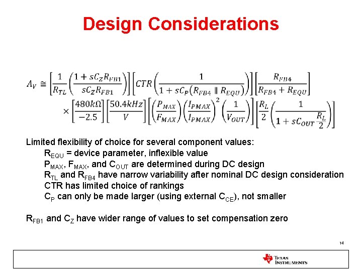
Design Considerations Limited flexibility of choice for several component values: REQU = device parameter, inflexible value PMAX, FMAX, and COUT are determined during DC design RTL and RFB 4 have narrow variability after nominal DC design consideration CTR has limited choice of rankings CP can only be made larger (using external CCE), not smaller RFB 1 and CZ have wider range of values to set compensation zero 14
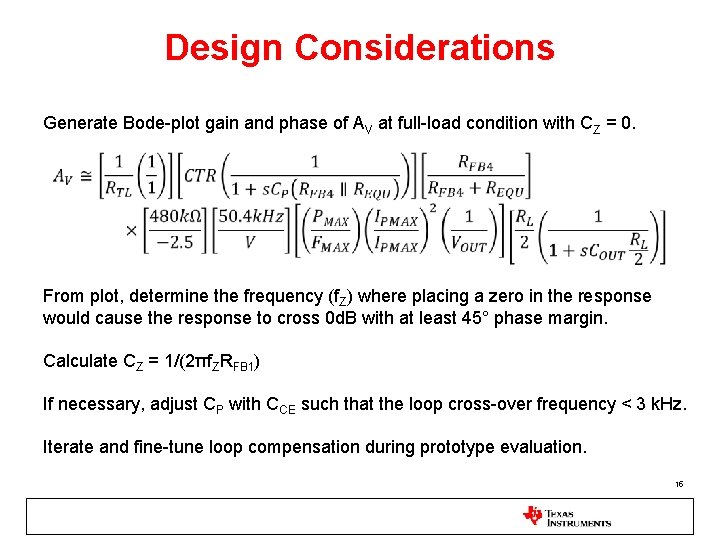
Design Considerations Generate Bode-plot gain and phase of AV at full-load condition with CZ = 0. From plot, determine the frequency (f. Z) where placing a zero in the response would cause the response to cross 0 d. B with at least 45° phase margin. Calculate CZ = 1/(2πf. ZRFB 1) If necessary, adjust CP with CCE such that the loop cross-over frequency < 3 k. Hz. Iterate and fine-tune loop compensation during prototype evaluation. 15
Simplifying Assumptions TL 431, CTR: The gain of these components do have high-frequency roll-off characteristics (pole) but are considered constant provided the loop crossover frequency is significantly lower than their respective pole frequencies. REQU is linearized from a piece-wise linear approximation of the VFB/IFB curve. The ESR-zero frequency of COUT is far above the loop crossover frequency. CFB 3 is more than 10 times larger than CP which causes its effect on compensation to be negligible. The product g. MRTL > 10000, which causes several terms to become negligible (g. M = transconductance of TL 431). 16
- Slides: 16