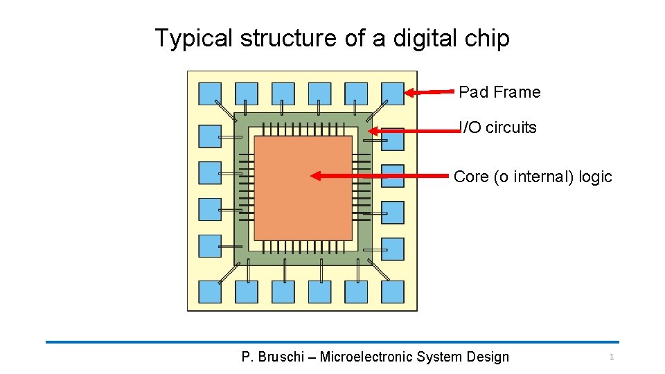
Typical structure of a digital chip Pad Frame


- Slides: 6

Typical structure of a digital chip Pad Frame I/O circuits Core (o internal) logic P. Bruschi – Microelectronic System Design 1

Latch-up layout rules: core logic Every part of a p-active area in an n-well must "see" at least one welltap with a maximum distance R Every part of an n-active area in the substrate (pwell) must "see" at least one substrate-tap with a maximum distance R P. Bruschi – Microelectronic System Design 2

I/O circuits: over-voltage risk Real case possible load / transmission line equivalent circuit Ideal case Vout Vdd I/O pad gnd In I/O circuits, the output termination can exceed the Vdd or gnd rails. This introduces additional risk of latch-up P. Bruschi – Microelectronic System Design 3

Injection of minority carriers when Vout exceeds Vdd, this diode is turned on when Vout drops below gnd, this diode is turned on Well: bases of the pnp BJT (collector of npn BJT) Substrate: bases of the npn BJT (collector of pnp BJT) P. Bruschi – Microelectronic System Design 4

Injection of minority carriers Injection of minority charge carriers into the parasitic BJTs bases may trigger the latch-up phenomenon Hole injection into the n-well when Vout > Vdd Electron injection into the substrate when Vout< 0 P. Bruschi – Microelectronic System Design 5

I/O devices: Guard Rings I/O circuits require additional protection against latch-up Guard rings are placed around the I/O devices in order to: I/O devices p+ (sub-tap) n+ (well tap) n-well p+ (sub. tap) gnd vdd gnd n-well p+ (sub. tap) • Reduce the resistance between drain/body diffusions to gnd (n. MOS) or Vdd (p. MOS) • Collect most of the minority carriers injected by one device before they reach neighboring devices These guard rings further reduce the effects of the I/O devices on the core logic P. Bruschi – Microelectronic System Design 6