Types of Field Effect Transistors The Classification FET
- Slides: 10

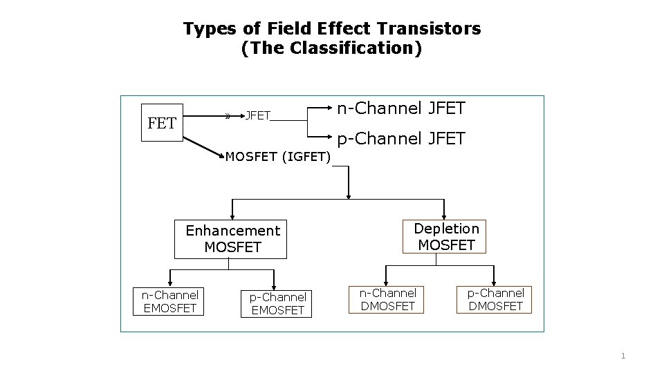
Types of Field Effect Transistors (The Classification) » FET JFET n-Channel JFET p-Channel JFET MOSFET (IGFET) Enhancement MOSFET n-Channel EMOSFET p-Channel EMOSFET Depletion MOSFET n-Channel DMOSFET p-Channel DMOSFET 1

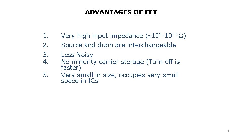
ADVANTAGES OF FET 1. Very high input impedance ( 109 -1012 ) 2. Source and drain are interchangeable 3. 4. Less Noisy No minority carrier storage (Turn off is faster) Very small in size, occupies very small space in ICs 5. 2

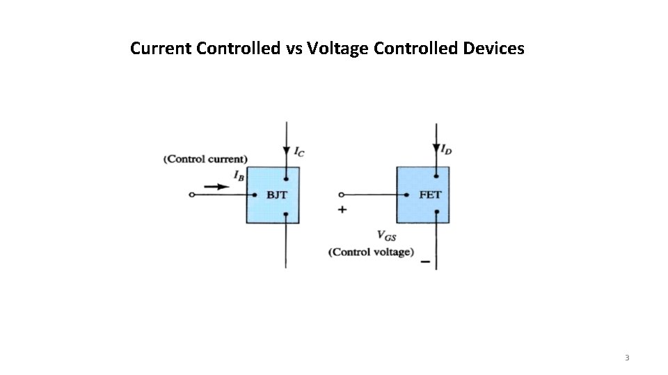
Current Controlled vs Voltage Controlled Devices 3

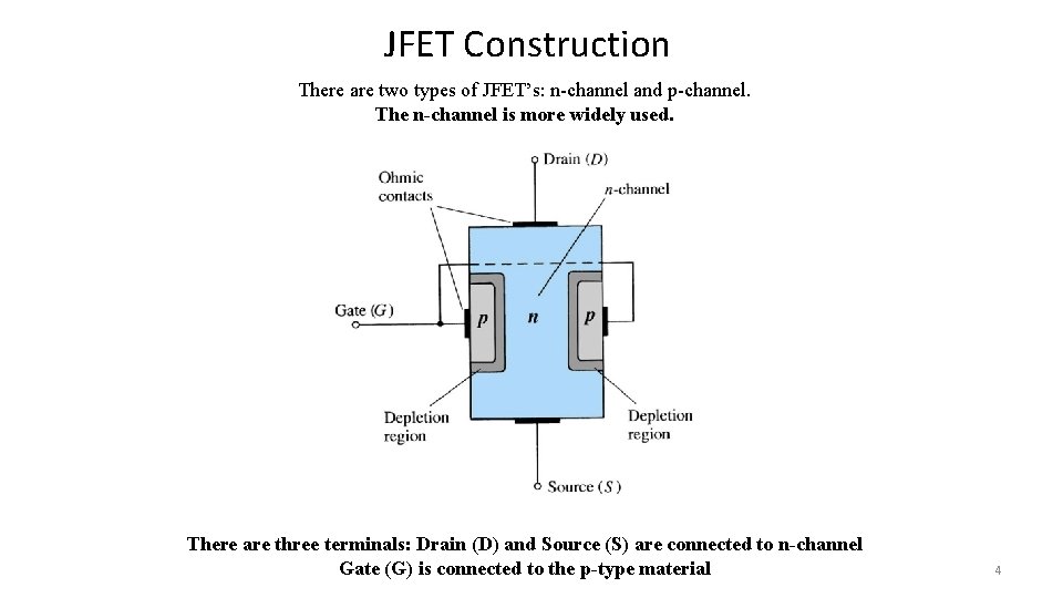
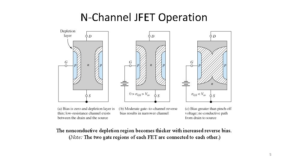
JFET Construction There are two types of JFET’s: n-channel and p-channel. The n-channel is more widely used. There are three terminals: Drain (D) and Source (S) are connected to n-channel Gate (G) is connected to the p-type material 4

N-Channel JFET Operation The nonconductive depletion region becomes thicker with increased reverse bias. (Note: The two gate regions of each FET are connected to each other. ) 5

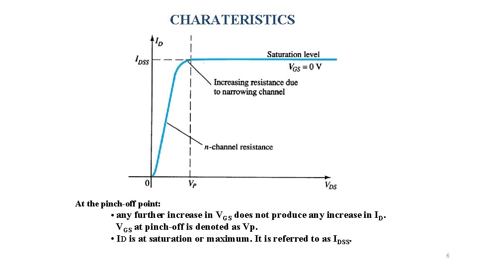
CHARATERISTICS At the pinch-off point: • any further increase in VGS does not produce any increase in ID. VGS at pinch-off is denoted as Vp. • ID is at saturation or maximum. It is referred to as IDSS. 6

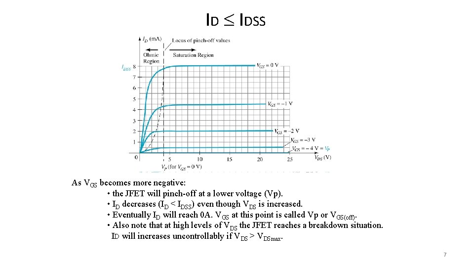
ID IDSS As VGS becomes more negative: • the JFET will pinch-off at a lower voltage (Vp). • ID decreases (ID < IDSS) even though VDS is increased. • Eventually ID will reach 0 A. VGS at this point is called Vp or VGS(off). • Also note that at high levels of VDS the JFET reaches a breakdown situation. ID will increases uncontrollably if VDS > VDSmax. 7

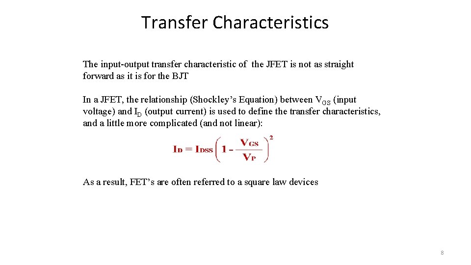
Transfer Characteristics The input-output transfer characteristic of the JFET is not as straight forward as it is for the BJT In a JFET, the relationship (Shockley’s Equation) between VGS (input voltage) and ID (output current) is used to define the transfer characteristics, and a little more complicated (and not linear): As a result, FET’s are often referred to a square law devices 8

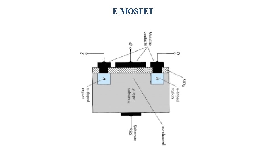
E-MOSFET

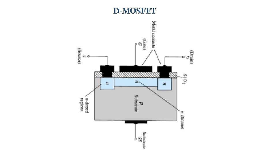
D-MOSFET