Trigger System Functions MasterSlave Operation Located in Readout


- Slides: 5

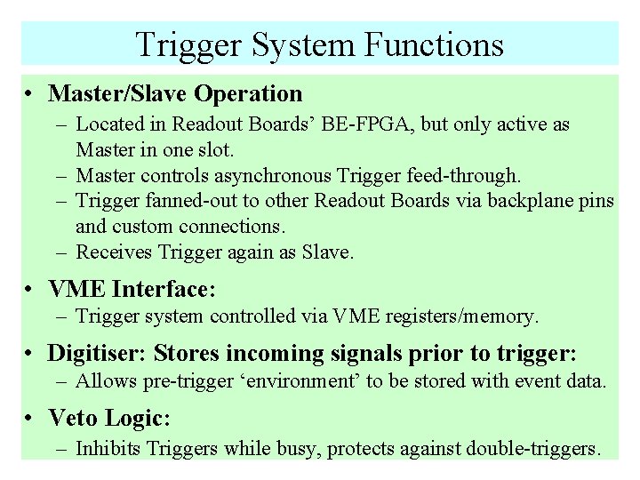
Trigger System Functions • Master/Slave Operation – Located in Readout Boards’ BE-FPGA, but only active as Master in one slot. – Master controls asynchronous Trigger feed-through. – Trigger fanned-out to other Readout Boards via backplane pins and custom connections. – Receives Trigger again as Slave. • VME Interface: – Trigger system controlled via VME registers/memory. • Digitiser: Stores incoming signals prior to trigger: – Allows pre-trigger ‘environment’ to be stored with event data. • Veto Logic: – Inhibits Triggers while busy, protects against double-triggers.

Trigger System Functions (Continued) • Interfaces to other slots and external devices: – May have back-of-crate card to provide fan-out & connector. – Some signals can generate interrupts (Beam. On/Off). – Able to delay outgoing external Triggers (~5 ns steps). • Stand-alone functions: – Periodic/Random Trigger, Clock generator. • Sequencer/Sink - Play/Record (pre-)trigger events: – 16 k. Bytes (clock periods) deep - pending FPGA utilisation. – Good for repeatability and fast trigger testing (sync. only). – Sink stores outgoing signals - provides software testability.

Trigger System Functional Diagram J 2 VME SEQ 1 x Beam. On START Edge Detect Beam On STOP Sync + Enable VME IRQ J 2 Internal Trig Osc + Randomiser IRQ 8 x Trigger VME BP LVDS 8 Out 4 x Pre. Trigger VME SEQ Pre-Trigger VME Sync + Enables Trigger Gate Generate 4 x SR Trigger Latch, Veto VME SEQ EXT NIM 16 In 4 x Activity VME Sync + Enables START STOP 4 x SR Width/ Delay 1 x Veto 8 x Counter Delays VME 160 MHz 6 x Spare Delayed Trig 1 16 Out SINK Delayed Trig 8 SINK SR ‘Digitiser’ ‘Sequencer’ + ‘Sink’ 32 bit Shift Registers (x 9) 16 KByte RAM 1 x Clock 4 x Spare 40 MHz 1 x Trigger LVDS 3 x Spare 5 In Sync + Enable EXT NIM VME Veto VME 4 x Trigger IRQ SINK VME SEQ J 0 Trigger Sync Clock Control VME BE FPGA - Trigger System (v 4 - 22/9/2003) 1 x Clock J 0 1 x Spare LVDS 2 Out

Trigger/Event Data Integration Event Data Store Front-End Data FE-BE Control & Transfer Trig 01 02 03 04 05 Pre-Triggers Trigger Processor Trigger Data Store 01 02 03 04 05 Readout Data Block Select & Build Backplane Data Transfer Header Block (Trig) Data Block (Event) Readout Data Block

Trigger Status • External Interface: Mostly specified. – Requires back-of-crate cable/board system finalised. • Trigger Processing System: Outline complete. – – Requirements understood. Overall code structure in place, but nuts-and-bolts not coded. More work required on asynchronous trigger transfer skew. Simulation of not started. • Integration with existing firmware: Started. – Able to edit existing FED design in HDL Designer. – Register Read/Write path understood. – Coupling to event data block header not understood.