
Tri Media TM 5250 Optimization Torsten Fink Manoj










- Slides: 71
Tri. Media TM 5250 Optimization Torsten Fink & Manoj Koul Tri. Media Center of Excellence January 2006
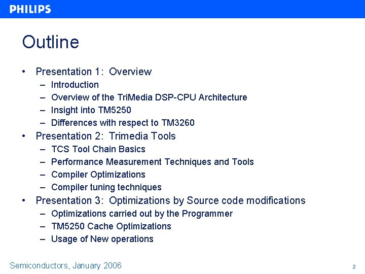
Outline • Presentation 1: Overview – – Introduction Overview of the Tri. Media DSP-CPU Architecture Insight into TM 5250 Differences with respect to TM 3260 • Presentation 2: Trimedia Tools – – TCS Tool Chain Basics Performance Measurement Techniques and Tools Compiler Optimizations Compiler tuning techniques • Presentation 3: Optimizations by Source code modifications – Optimizations carried out by the Programmer – TM 5250 Cache Optimizations – Usage of New operations Semiconductors, January 2006 2
Introduction Semiconductors, January 2006 3
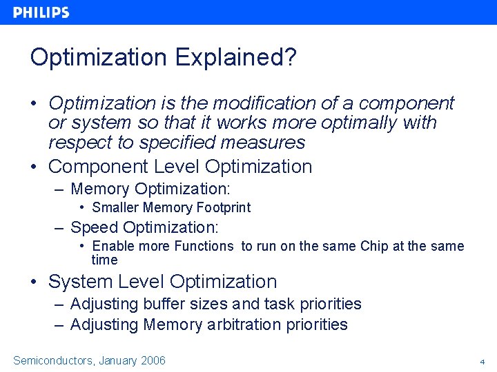
Optimization Explained? • Optimization is the modification of a component or system so that it works more optimally with respect to specified measures • Component Level Optimization – Memory Optimization: • Smaller Memory Footprint – Speed Optimization: • Enable more Functions to run on the same Chip at the same time • System Level Optimization – Adjusting buffer sizes and task priorities – Adjusting Memory arbitration priorities Semiconductors, January 2006 4
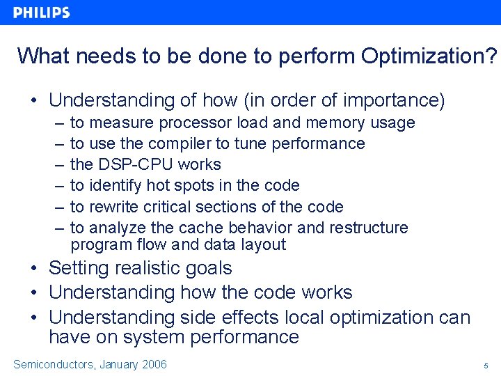
What needs to be done to perform Optimization? • Understanding of how (in order of importance) – – – to measure processor load and memory usage to use the compiler to tune performance the DSP-CPU works to identify hot spots in the code to rewrite critical sections of the code to analyze the cache behavior and restructure program flow and data layout • Setting realistic goals • Understanding how the code works • Understanding side effects local optimization can have on system performance Semiconductors, January 2006 5
Introduction • This section of the presentation explains how the Tri. Media DSP-CPU architecture has evolved since TM 3260. • Focus on Key differences between TM 3260 & TM 5250. • The CPUs explained are – TM 3260 – TM 5250 – TM 3270 (Introduction only) Semiconductors, January 2006 6
So. Cs with Tri. Media CPUs Some examples
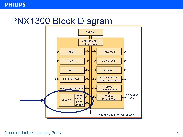
PNX 1300 Block Diagram SDRAM MAIN MEMORY INTERFACE VIDEO IN VIDEO OUT AUDIO IN AUDIO OUT TIMERS SPDIF OUT I 2 C INTERFACE SYNCHRONOUS SERIAL INTERFACE VLD COPROCESSOR IMAGE COPROCESSOR VLIW CPU INSTR CACHE PCI/XIO INTERFACE TO PCI/XIO BUS DATA CACHE INTERNAL BUS (DATA HIGHWAY) Semiconductors, January 2006 8
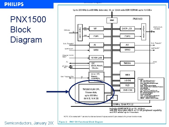
PNX 1500 Block Diagram Semiconductors, January 2006 9
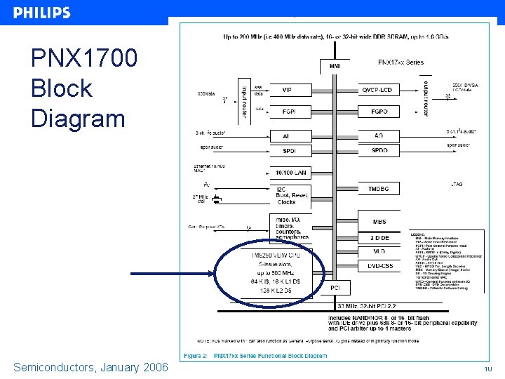
PNX 1700 Block Diagram Semiconductors, January 2006 10
Tri. Media Core Architecture Overview
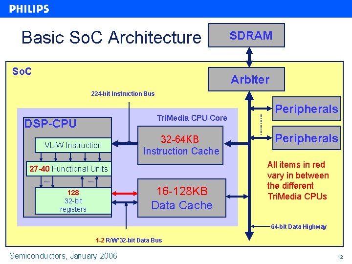
Basic So. C Architecture So. C SDRAM Arbiter 224 -bit Instruction Bus Tri. Media CPU Core DSP-CPU VLIW Instruction 32 -64 KB Instruction Cache 27 -40 Functional Units 16 -128 KB Data Cache 128 32 -bit registers Peripherals All items in red vary in between the different Tri. Media CPUs 64 -bit Data Highway 1 -2 R/W*32 -bit Data Bus Semiconductors, January 2006 12
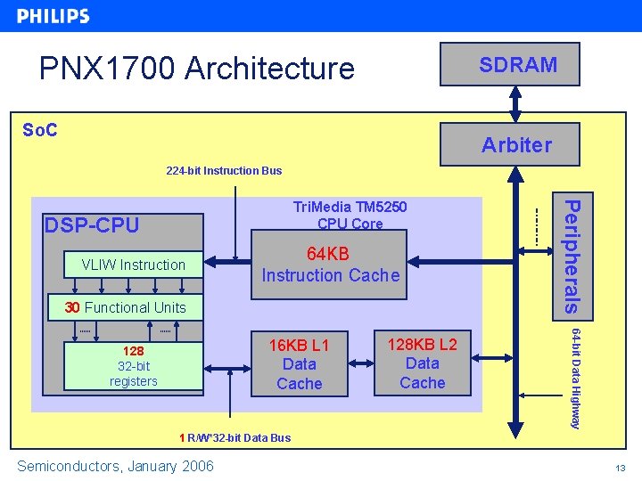
PNX 1700 Architecture SDRAM So. C Arbiter 224 -bit Instruction Bus DSP-CPU VLIW Instruction 64 KB Instruction Cache 30 Functional Units 128 KB L 2 Data Cache 64 -bit Data Highway 16 KB L 1 Data Cache 128 32 -bit registers Peripherals Tri. Media TM 5250 CPU Core 1 R/W*32 -bit Data Bus Semiconductors, January 2006 13
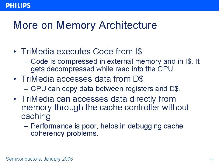
More on Memory Architecture • Tri. Media executes Code from I$ – Code is compressed in external memory and in I$. It gets decompressed while read into the CPU. • Tri. Media accesses data from D$ – CPU can copy data between registers and D$. • Tri. Media can accesses data directly from memory through the cache controller without caching – Performance is poor, helps in debugging cache coherency problems. Semiconductors, January 2006 14
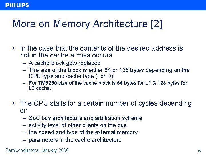
More on Memory Architecture [2] • In the case that the contents of the desired address is not in the cache a miss occurs – A cache block gets replaced – The size of the block is either 64 or 128 bytes depending on the CPU type and cache type (I or D) – For TM 5250 size of the cache block is 64 bytes for L 1 & 128 bytes for L 2 cache. • The CPU stalls for a certain number of cycles depending on – – So. C bus architecture and arbitration scheme activity level of other clients on the bus the speed and type of the external memory parameters in the cache architecture Semiconductors, January 2006 15
Approach of this presentation • First focus on difference in Functional Units • Then look at difference in the Cache Architectures • Then look at other improvements Semiconductors, January 2006 16
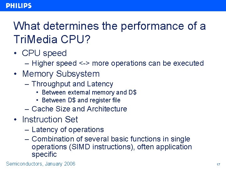
What determines the performance of a Tri. Media CPU? • CPU speed – Higher speed <-> more operations can be executed • Memory Subsystem – Throughput and Latency • Between external memory and D$ • Between D$ and register file – Cache Size and Architecture • Instruction Set – Latency of operations – Combination of several basic functions in single operations (SIMD instructions), often application specific Semiconductors, January 2006 17
VLIW Core and Functional Units
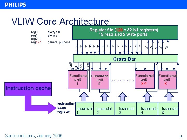
VLIW Core Architecture reg 0 reg 1 reg 2 reg 127 Register file (128 x 32 bit registers) 15 read and 5 write ports always 0 always 1 general purpose R R R R W W W Cross Bar result src 2 src 1 guard Functional unit 1 2 Instruction cache Instruction issue Issue slot register 1 Semiconductors, January 2006 . . . . Issue slot 2 Issue slot 3 Functional unit X-1 Issue slot 4 Functional unit X Issue slot 5 19
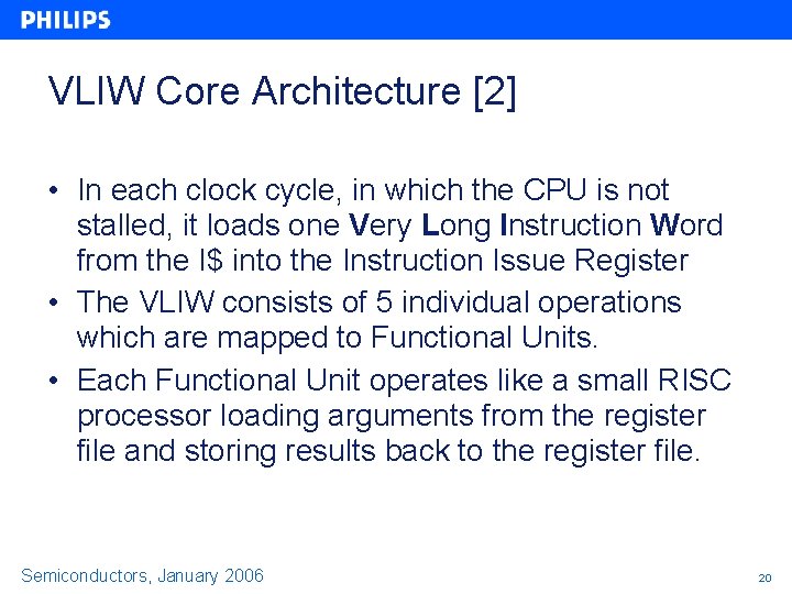
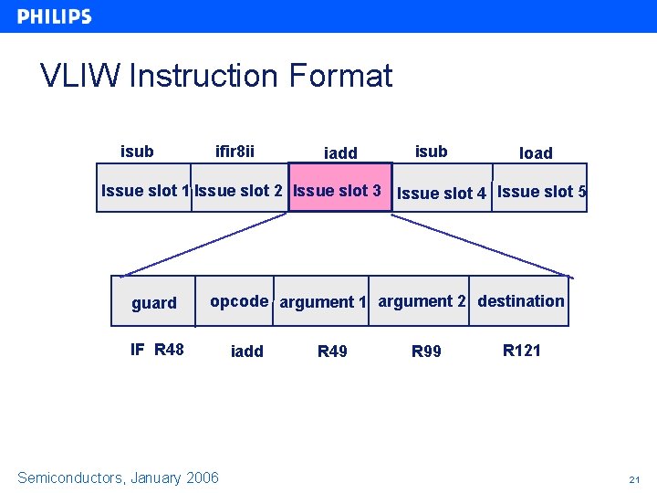
VLIW Core Architecture [2] • In each clock cycle, in which the CPU is not stalled, it loads one Very Long Instruction Word from the I$ into the Instruction Issue Register • The VLIW consists of 5 individual operations which are mapped to Functional Units. • Each Functional Unit operates like a small RISC processor loading arguments from the register file and storing results back to the register file. Semiconductors, January 2006 20
VLIW Instruction Format isub ifir 8 ii iadd isub load Issue slot 1 Issue slot 2 Issue slot 3 Issue slot 4 Issue slot 5 guard opcode argument 1 argument 2 destination IF R 48 Semiconductors, January 2006 iadd R 49 R 99 R 121 21
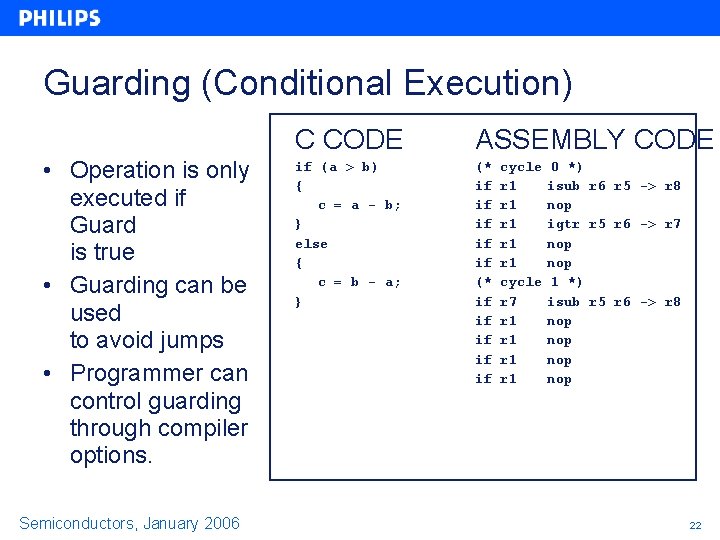
Guarding (Conditional Execution) • Operation is only executed if Guard is true • Guarding can be used to avoid jumps • Programmer can control guarding through compiler options. Semiconductors, January 2006 C CODE ASSEMBLY CODE if (a > b) { c = a - b; } else { c = b - a; } (* if if if cycle r 1 r 1 r 1 cycle r 7 r 1 r 1 0 *) isub r 6 r 5 -> r 8 nop igtr r 5 r 6 -> r 7 nop 1 *) isub r 5 r 6 -> r 8 nop nop 22
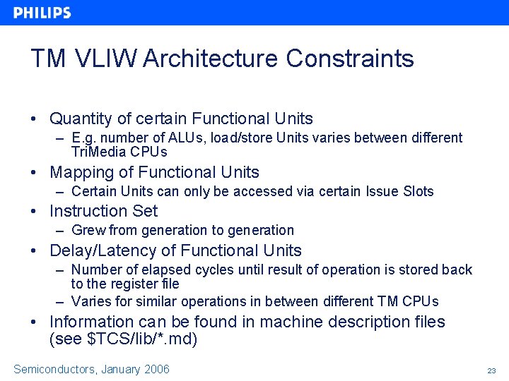
TM VLIW Architecture Constraints • Quantity of certain Functional Units – E. g. number of ALUs, load/store Units varies between different Tri. Media CPUs • Mapping of Functional Units – Certain Units can only be accessed via certain Issue Slots • Instruction Set – Grew from generation to generation • Delay/Latency of Functional Units – Number of elapsed cycles until result of operation is stored back to the register file – Varies for similar operations in between different TM CPUs • Information can be found in machine description files (see $TCS/lib/*. md) Semiconductors, January 2006 23
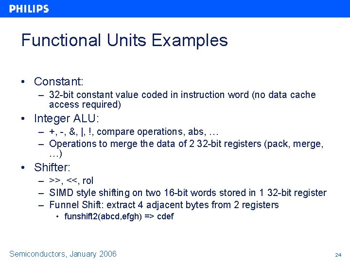
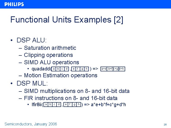
Functional Units Examples • Constant: – 32 -bit constant value coded in instruction word (no data cache access required) • Integer ALU: – +, -, &, |, !, compare operations, abs, … – Operations to merge the data of 2 32 -bit registers (pack, merge, …) • Shifter: – >>, <<, rol – SIMD style shifting on two 16 -bit words stored in 1 32 -bit register – Funnel Shift: extract 4 adjacent bytes from 2 registers • funshift 2(abcd, efgh) => cdef Semiconductors, January 2006 24
Functional Units Examples [2] • DSP ALU: – Saturation arithmetic – Clipping operations – SIMD ALU operations • quadadd( a b c d , e f g h ) => a+e b+f c+g d+h – Motion Estimation operations • DSP MUL: – SIMD multiplications on 8 - and 16 -bit data – FIR instructions on 8 - and 16 -bit data • Ifir 8 ii( a b c Semiconductors, January 2006 d , e f g h ) => a*e+b*f+c*g+d*h 25
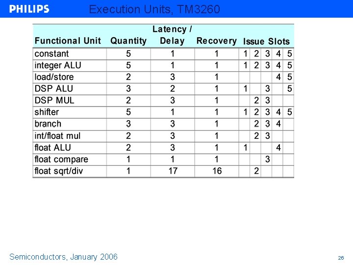
Execution Units, TM 3260 Semiconductors, January 2006 26
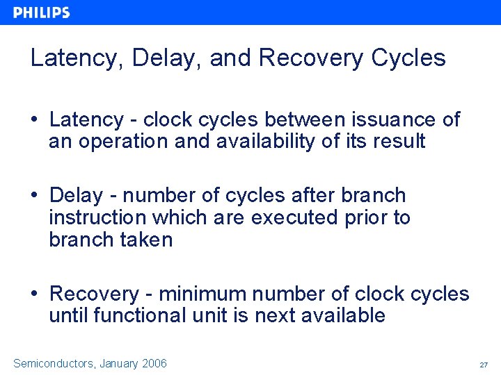
Latency, Delay, and Recovery Cycles • Latency - clock cycles between issuance of an operation and availability of its result • Delay - number of cycles after branch instruction which are executed prior to branch taken • Recovery - minimum number of clock cycles until functional unit is next available Semiconductors, January 2006 27
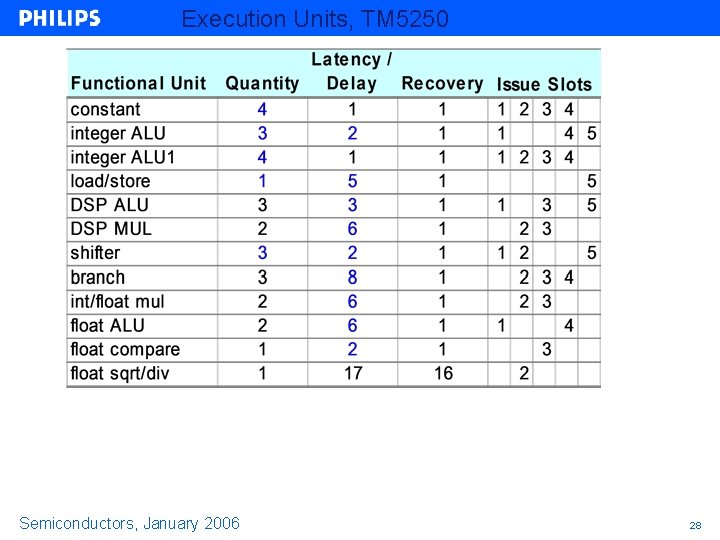
Execution Units, TM 5250 Semiconductors, January 2006 28
What can you learn from these tables? • Avoid % and / in your code! – Latency time 17 and recovery time 16 cycles! • Floating Point vs. Fixed Point – No difference in multipliers – 4 integer ALUs with 1 cycle latency – 2 floating point ALUs with 6 cycles delay – For recursive algorithms fixed point is likely to be better, for FIR structures there is no big difference. Semiconductors, January 2006 29
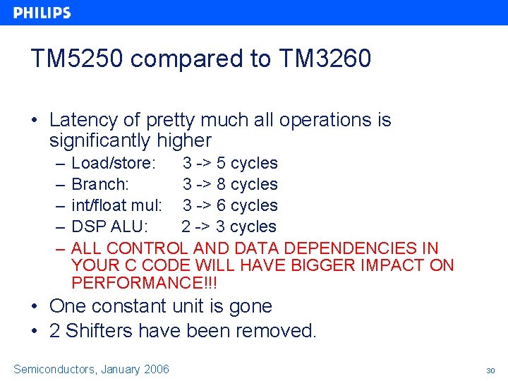
TM 5250 compared to TM 3260 • Latency of pretty much all operations is significantly higher – – – Load/store: 3 -> 5 cycles Branch: 3 -> 8 cycles int/float mul: 3 -> 6 cycles DSP ALU: 2 -> 3 cycles ALL CONTROL AND DATA DEPENDENCIES IN YOUR C CODE WILL HAVE BIGGER IMPACT ON PERFORMANCE!!! • One constant unit is gone • 2 Shifters have been removed. Semiconductors, January 2006 30
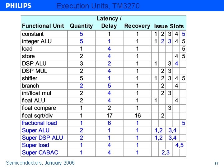
Execution Units, TM 3270 Semiconductors, January 2006 31
Brief Overview of Data Types • The next two pages summarize the data types natively supported by the HW and data types supported by SW via emulation. • Remember: all data is stored in 32 -bit registers! Semiconductors, January 2006 32
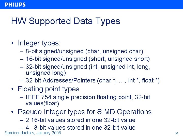
HW Supported Data Types • Integer types: – 8 -bit signed/unsigned (char, unsigned char) – 16 -bit signed/unsigned (short, unsigned short) – 32 -bit signed/unsigned (int, unsigned int, long, unsigned long) – 32 -bit Addresses/Pointers (char *, …, int *, float *) • Floating point types – IEEE 754 single precision floating point, 32 -bit values(float) • Pseudo Integer types for SIMD Operations – 2 16 -bit values stored in one 32 -bit value – 4 8 -bit values stored in one 32 -bit value Semiconductors, January 2006 33
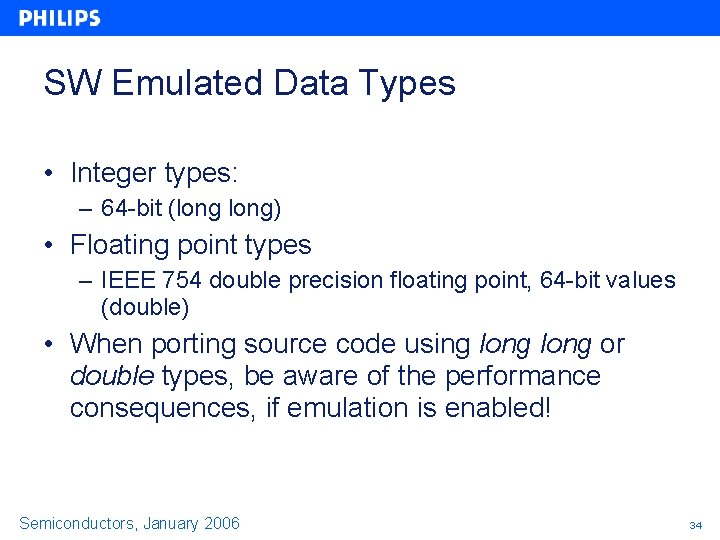
SW Emulated Data Types • Integer types: – 64 -bit (long) • Floating point types – IEEE 754 double precision floating point, 64 -bit values (double) • When porting source code using long or double types, be aware of the performance consequences, if emulation is enabled! Semiconductors, January 2006 34
Memory Architecture
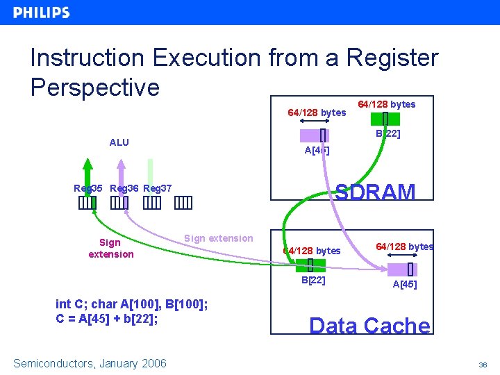
Instruction Execution from a Register Perspective 64/128 bytes B[22] ALU A[45] SDRAM Reg 35 Reg 36 Reg 37 Sign extension int C; char A[100], B[100]; C = A[45] + b[22]; Semiconductors, January 2006 64/128 bytes B[22] A[45] Data Cache 36
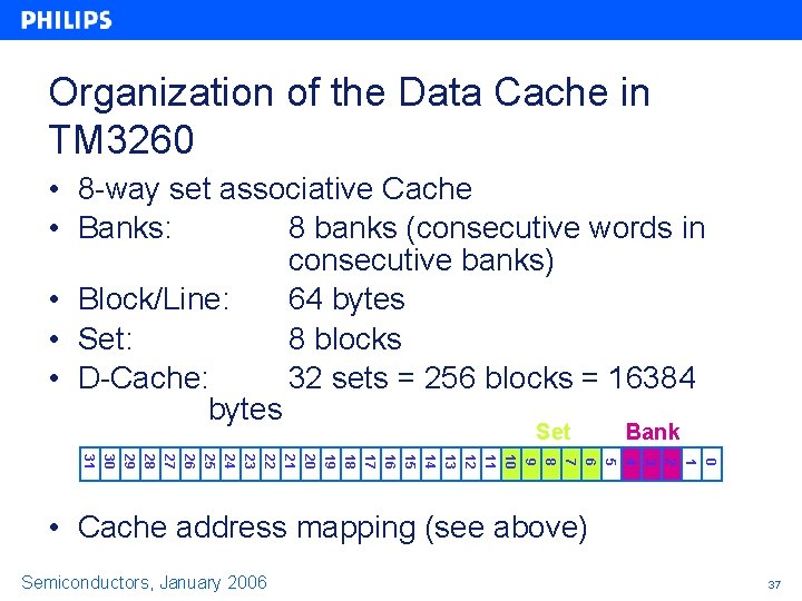
Organization of the Data Cache in TM 3260 • 8 -way set associative Cache • Banks: 8 banks (consecutive words in consecutive banks) • Block/Line: 64 bytes • Set: 8 blocks • D-Cache: 32 sets = 256 blocks = 16384 bytes Set Bank 0 1 2 3 4 5 6 7 8 9 10 11 12 13 14 15 16 17 18 19 20 21 22 23 24 25 26 27 28 29 30 31 • Cache address mapping (see above) Semiconductors, January 2006 37
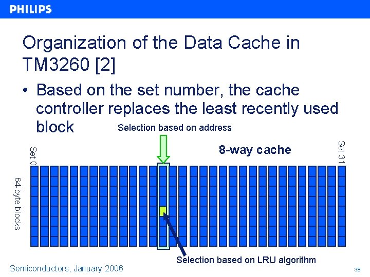
Organization of the Data Cache in TM 3260 [2] • Based on the set number, the cache controller replaces the least recently used Selection based on address block Set 31 Set 0 8 -way cache 64 -byte blocks Semiconductors, January 2006 Selection based on LRU algorithm 38
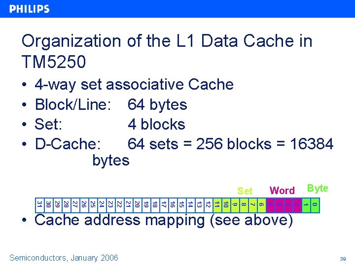
Organization of the L 1 Data Cache in TM 5250 • • 4 -way set associative Cache Block/Line: 64 bytes Set: 4 blocks D-Cache: 64 sets = 256 blocks = 16384 bytes Set Word Byte 0 1 2 3 4 5 6 7 8 9 10 11 12 13 14 15 16 17 18 19 20 21 22 23 24 25 26 27 28 29 30 31 • Cache address mapping (see above) Semiconductors, January 2006 39
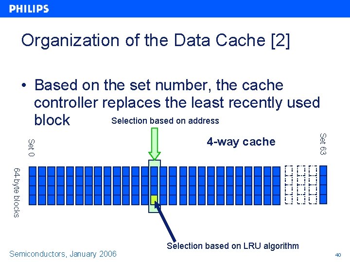
Organization of the Data Cache [2] • Based on the set number, the cache controller replaces the least recently used Selection based on address block Set 63 Set 0 4 -way cache 64 -byte blocks Semiconductors, January 2006 Selection based on LRU algorithm 40
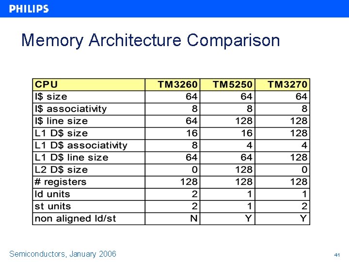
Memory Architecture Comparison Semiconductors, January 2006 41
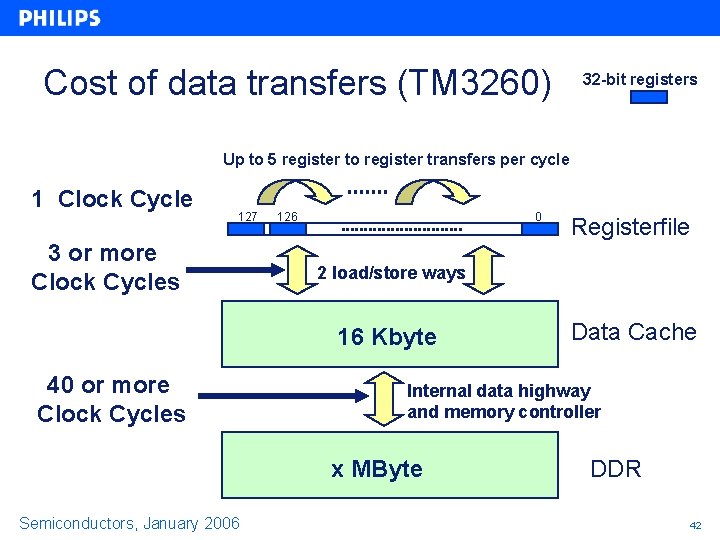
Cost of data transfers (TM 3260) 32 -bit registers Up to 5 register to register transfers per cycle 1 Clock Cycle 127 3 or more Clock Cycles 126 0 2 load/store ways 16 Kbyte 40 or more Clock Cycles Data Cache Internal data highway and memory controller x MByte Semiconductors, January 2006 Registerfile DDR 42
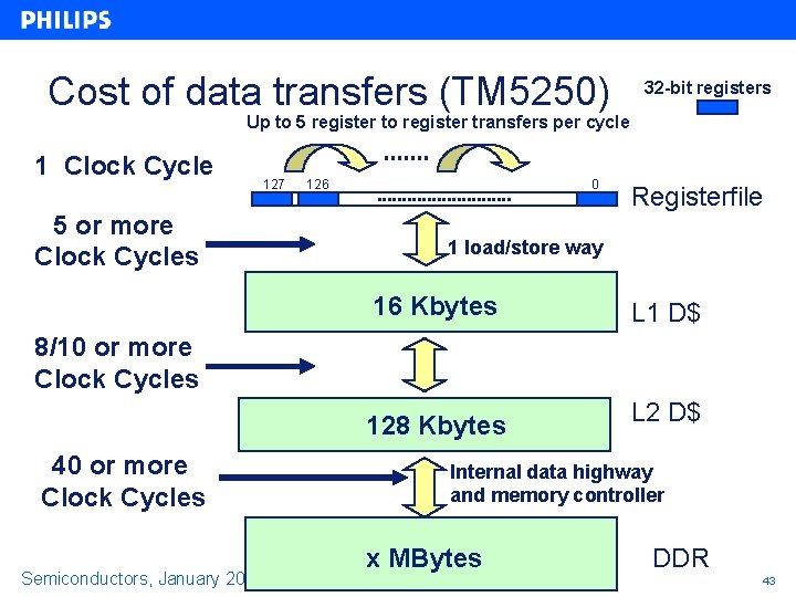
Cost of data transfers (TM 5250) 32 -bit registers Up to 5 register to register transfers per cycle 1 Clock Cycle 127 5 or more Clock Cycles 126 0 Registerfile 1 load/store way 16 Kbytes L 1 D$ 128 Kbytes L 2 D$ 8/10 or more Clock Cycles 40 or more Clock Cycles Semiconductors, January 2006 Internal data highway and memory controller x MBytes DDR 43
Additional CPU specific Information
TM 3260
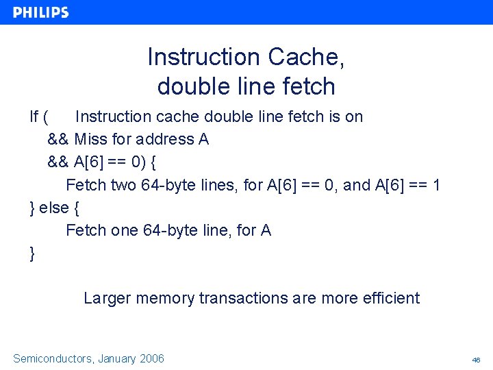
Instruction Cache, double line fetch If ( Instruction cache double line fetch is on && Miss for address A && A[6] == 0) { Fetch two 64 -byte lines, for A[6] == 0, and A[6] == 1 } else { Fetch one 64 -byte line, for A } Larger memory transactions are more efficient Semiconductors, January 2006 46
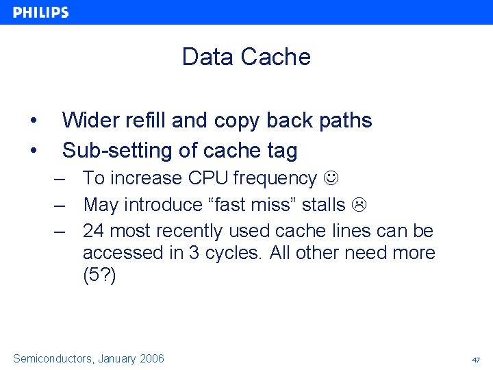
Data Cache • • Wider refill and copy back paths Sub-setting of cache tag – To increase CPU frequency – May introduce “fast miss” stalls – 24 most recently used cache lines can be accessed in 3 cycles. All other need more (5? ) Semiconductors, January 2006 47
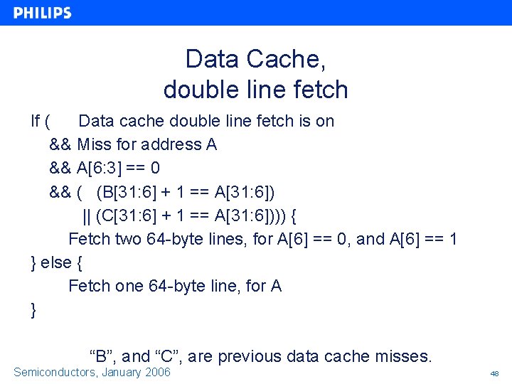
Data Cache, double line fetch If ( Data cache double line fetch is on && Miss for address A && A[6: 3] == 0 && ( (B[31: 6] + 1 == A[31: 6]) || (C[31: 6] + 1 == A[31: 6]))) { Fetch two 64 -byte lines, for A[6] == 0, and A[6] == 1 } else { Fetch one 64 -byte line, for A } “B”, and “C”, are previous data cache misses. Semiconductors, January 2006 48
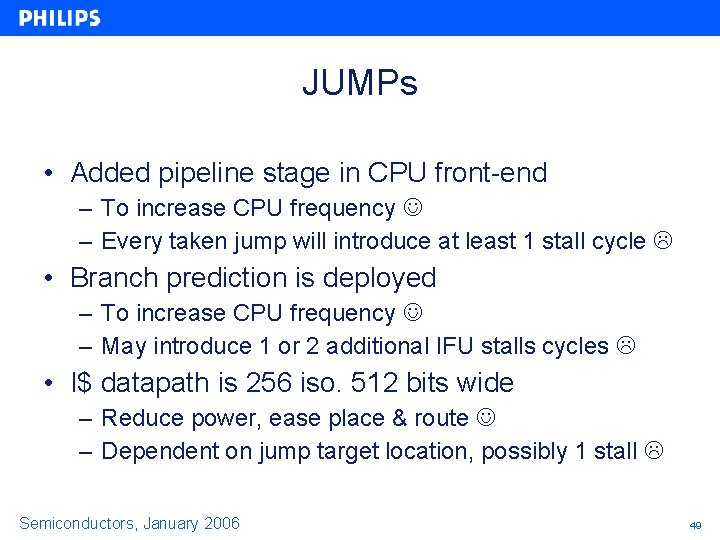
JUMPs • Added pipeline stage in CPU front-end – To increase CPU frequency – Every taken jump will introduce at least 1 stall cycle • Branch prediction is deployed – To increase CPU frequency – May introduce 1 or 2 additional IFU stalls cycles • I$ datapath is 256 iso. 512 bits wide – Reduce power, ease place & route – Dependent on jump target location, possibly 1 stall Semiconductors, January 2006 49
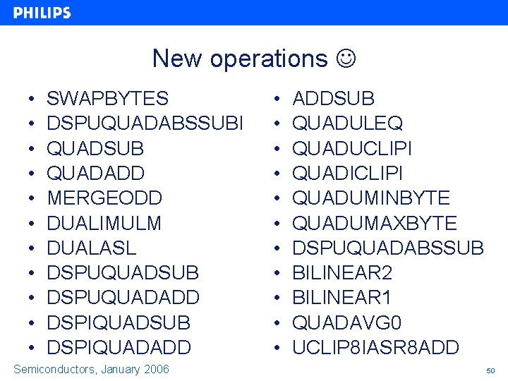
New operations • • • SWAPBYTES DSPUQUADABSSUBI QUADSUB QUADADD MERGEODD DUALIMULM DUALASL DSPUQUADSUB DSPUQUADADD DSPIQUADSUB DSPIQUADADD Semiconductors, January 2006 • • • ADDSUB QUADULEQ QUADUCLIPI QUADICLIPI QUADUMINBYTE QUADUMAXBYTE DSPUQUADABSSUB BILINEAR 2 BILINEAR 1 QUADAVG 0 UCLIP 8 IASR 8 ADD 50
TM 5250
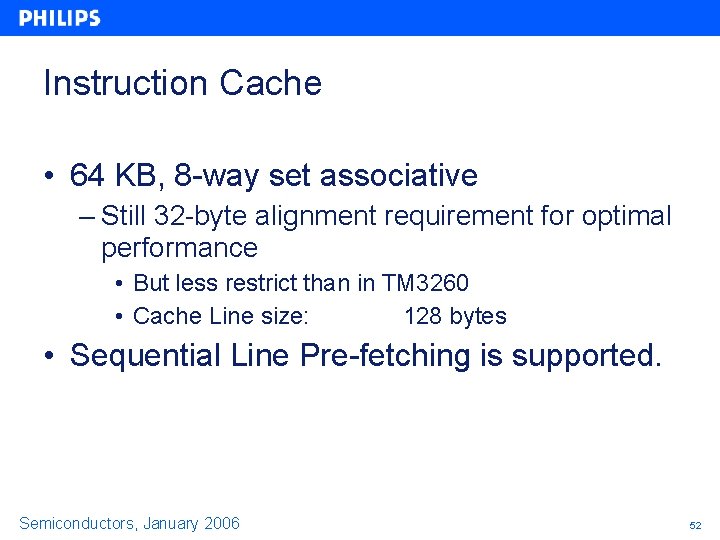
Instruction Cache • 64 KB, 8 -way set associative – Still 32 -byte alignment requirement for optimal performance • But less restrict than in TM 3260 • Cache Line size: 128 bytes • Sequential Line Pre-fetching is supported. Semiconductors, January 2006 52
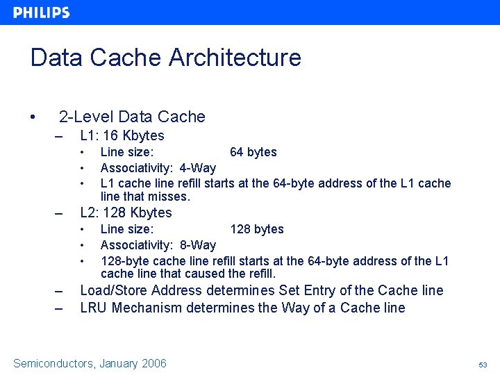
Data Cache Architecture • 2 -Level Data Cache – L 1: 16 Kbytes • • • – L 2: 128 Kbytes • • • – – Line size: 64 bytes Associativity: 4 -Way L 1 cache line refill starts at the 64 -byte address of the L 1 cache line that misses. Line size: 128 bytes Associativity: 8 -Way 128 -byte cache line refill starts at the 64 -byte address of the L 1 cache line that caused the refill. Load/Store Address determines Set Entry of the Cache line LRU Mechanism determines the Way of a Cache line Semiconductors, January 2006 53
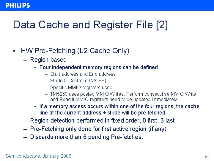
Data Cache and Register File [2] • HW Pre-Fetching (L 2 Cache Only) – Region based • Four independent memory regions can be defined – – Start address and End address Stride & Control (ON/OFF) Specific MMIO registers used. TM 5250 uses posted MMIO Writes. Perform consecutive MMIO Write and Read if MMIO registers need to be updated immediately. • If a memory access occurs within one of the four regions, the cache line at the current address + stride will be pre-fetched – Region detection performed in fixed order, 0 first, 3 last – Pre-Fetching only done for first active region (if any) – Discards more than 6 pending Pre-fetches. Semiconductors, January 2006 54
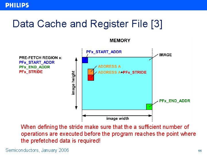
Data Cache and Register File [3] When defining the stride make sure that the a sufficient number of operations are executed before the program reaches the point where the prefetched data is required! Semiconductors, January 2006 55
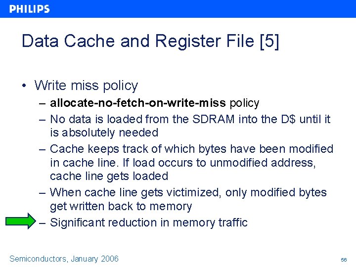
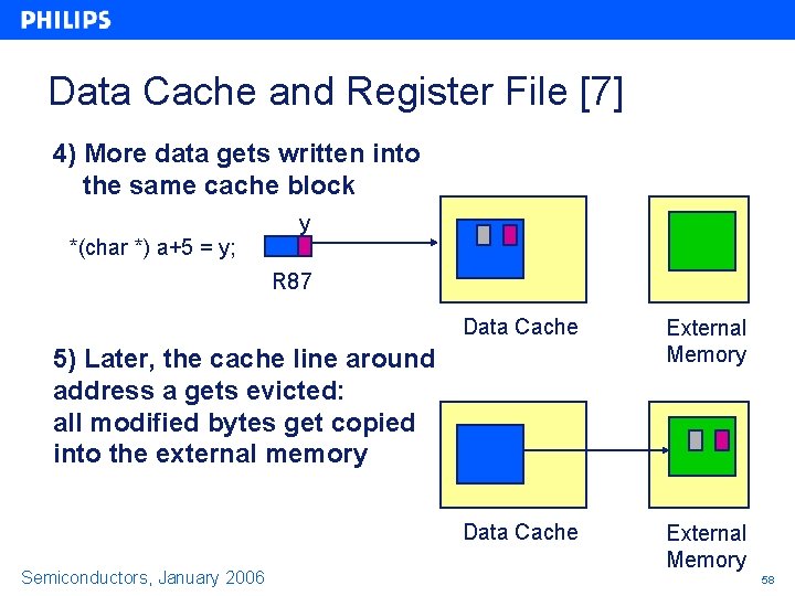
Data Cache and Register File [5] • Write miss policy – allocate-no-fetch-on-write-miss policy – No data is loaded from the SDRAM into the D$ until it is absolutely needed – Cache keeps track of which bytes have been modified in cache line. If load occurs to unmodified address, cache line gets loaded – When cache line gets victimized, only modified bytes get written back to memory – Significant reduction in memory traffic Semiconductors, January 2006 56
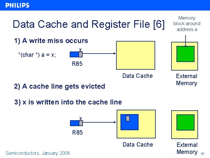
Data Cache and Register File [6] Memory block around address a 1) A write miss occurs *(char *) a = x; x R 85 Data Cache External Memory 2) A cache line gets evicted 3) x is written into the cache line x R 85 Semiconductors, January 2006 57
Data Cache and Register File [7] 4) More data gets written into the same cache block *(char *) a+5 = y; y R 87 Data Cache External Memory 5) Later, the cache line around address a gets evicted: all modified bytes get copied into the external memory Semiconductors, January 2006 58
Data Cache and Register File [8] • Non aligned load/store – 32 -bit and 16 -bit values can be read from any byte address (and also written to any) – Expect huge improvement for video • Save funshifts for motion estimation/compensation • Save loads – Probably less impact on audio • Might help for 16 -bit filtering Semiconductors, January 2006 59
Data Cache and Register File [9] • New allocd_set instruction – allocd_set(address, data) – Creates a cache line (in which address is located) – Fills the entire cache line with the value of data (32 -bit) – Can be used to implement memset() etc. Semiconductors, January 2006 60
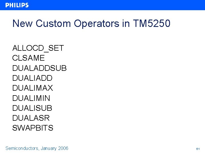
New Custom Operators in TM 5250 ALLOCD_SET CLSAME DUALADDSUB DUALIADD DUALIMAX DUALIMIN DUALISUB DUALASR SWAPBITS Semiconductors, January 2006 61
TM 3270
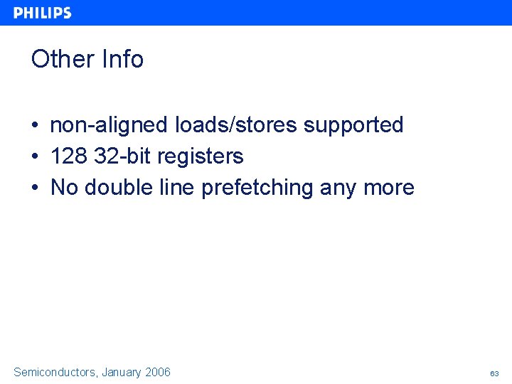
Other Info • non-aligned loads/stores supported • 128 32 -bit registers • No double line prefetching any more Semiconductors, January 2006 63
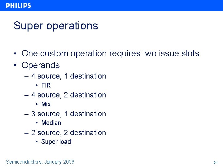
Super operations • One custom operation requires two issue slots • Operands – 4 source, 1 destination • FIR – 4 source, 2 destination • Mix – 3 source, 1 destination • Median – 2 source, 2 destination • Super load Semiconductors, January 2006 64
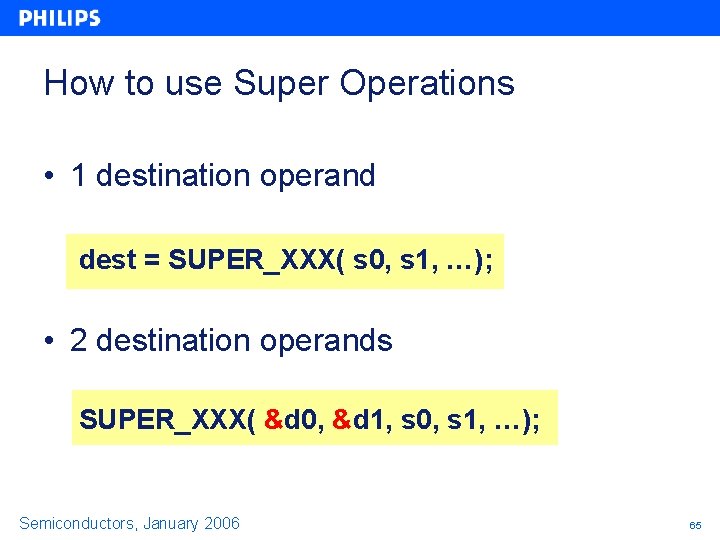
How to use Super Operations • 1 destination operand dest = SUPER_XXX( s 0, s 1, …); • 2 destination operands SUPER_XXX( &d 0, &d 1, s 0, s 1, …); Semiconductors, January 2006 65
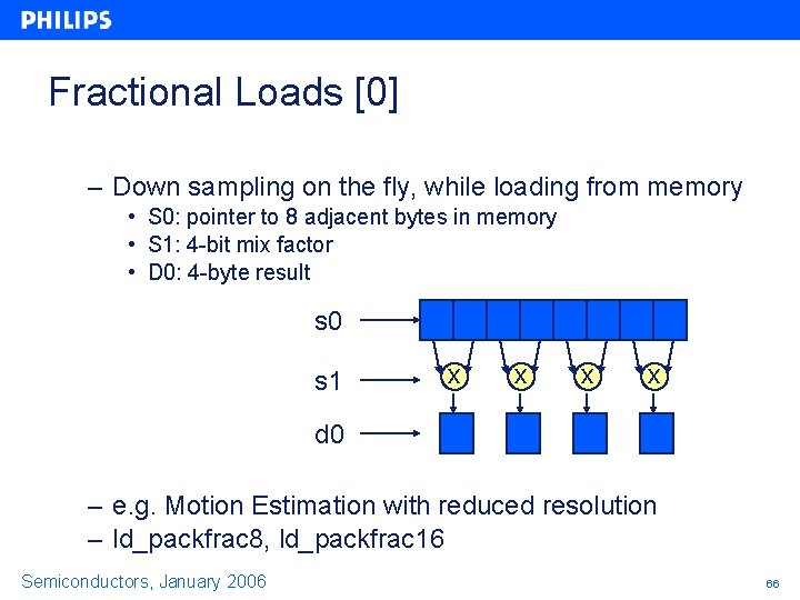
Fractional Loads [0] – Down sampling on the fly, while loading from memory • S 0: pointer to 8 adjacent bytes in memory • S 1: 4 -bit mix factor • D 0: 4 -byte result s 0 s 1 x x d 0 – e. g. Motion Estimation with reduced resolution – ld_packfrac 8, ld_packfrac 16 Semiconductors, January 2006 66
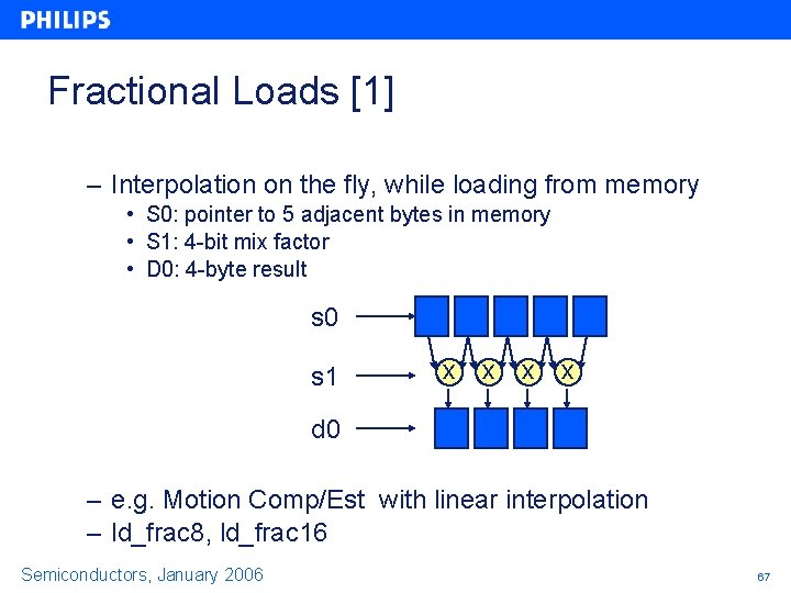
Fractional Loads [1] – Interpolation on the fly, while loading from memory • S 0: pointer to 5 adjacent bytes in memory • S 1: 4 -bit mix factor • D 0: 4 -byte result s 0 s 1 x x d 0 – e. g. Motion Comp/Est with linear interpolation – ld_frac 8, ld_frac 16 Semiconductors, January 2006 67
Super Loads • Load 8 bytes from memory address and store them in two registers • 3 address modes supported – Indexed, super_ld 32 r – Displacement, super_ld 32 d – Scaled, super_ld 32 x – Programmer has explicit control! • For normal loads, the compiler decides Semiconductors, January 2006 68
FIR with scaling, rounding, and clipping • E. g. : iclip 16 asr 14 scale 16 – Dual multiplication of 16 bit values – Useful for transforms and quantization Semiconductors, January 2006 69
Super CABAC instructions • 5 new instructions to accelerate H. 264 decoding Semiconductors, January 2006 70
New Super Operations for Video Processing • Quad Median Filters in one instruction • Several new mixing instructions Semiconductors, January 2006 71