Transmission Line Effects in High Speed Digital PCBs

Transmission Line Effects in High Speed Digital PCBs 中華大學 通訊系 田慶誠 tien@chu. edu. tw 03 5186030 中華大學 通訊系 1

Introduction of Waves § Vp: Phase velocity 中華大學 通訊系 2
 § 定义:流入流出的电流和相位一样,没有差值 § (1)")
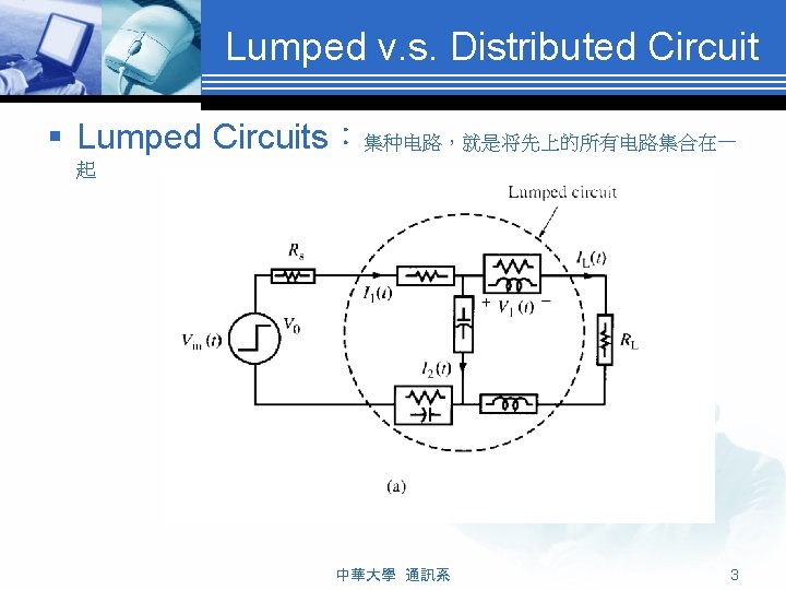
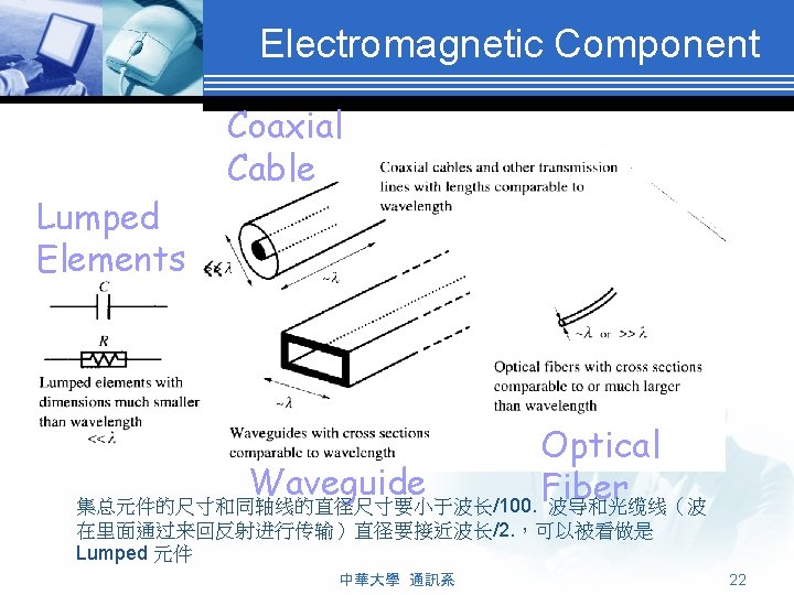
Lumped v. s. Distributed Circuit § Definitions of lumped element(RLC) § 定义:流入流出的电流和相位一样,没有差值 § (1) Input current amplitude () = Output current amplitude § (2) Input current phase = Output current phase 中華大學 通訊系 4
分散电路 中華大學 通訊系 5")
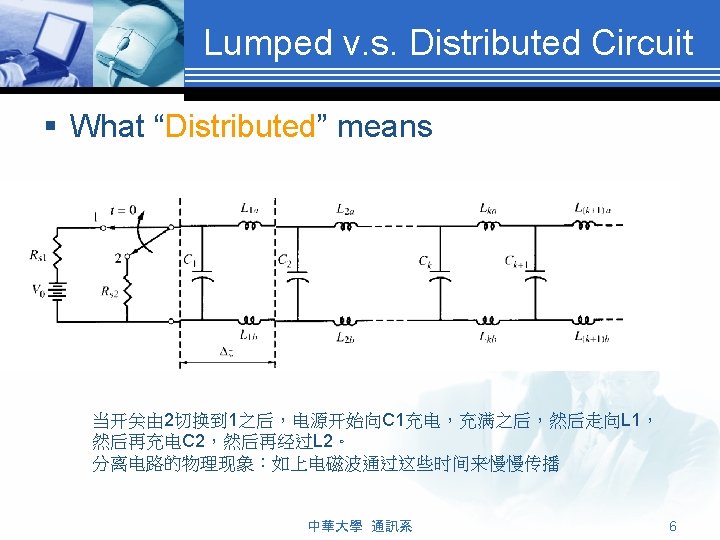
Lumped v. s. Distributed Circuit § Distributed Circuit()分散电路 中華大學 通訊系 5

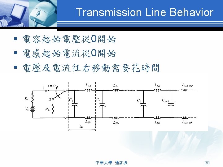
Rise Time v. s. Travel Time § Tr: Rise Time Td: Delay Time Vin过Rs,从l端左边到右边的时延是td 中華大學 通訊系 7

Digital Interconnection Rules § 數位 程師的 Rule of thumb § Signal path can be treated as: A lumped element, (RLC单器件) if Tr > 6 Td § (Short ckt, series resistor, shunt capacitor) A lumped model, if 2. 5 < Tr/Td < 6 § (Series inductor with shunt capacitor)(集总式原件 的组合) A distributed model, if Tr < 2. 5 Td § (Transmission Line or multi-section LC model) 中華大學 通訊系 8
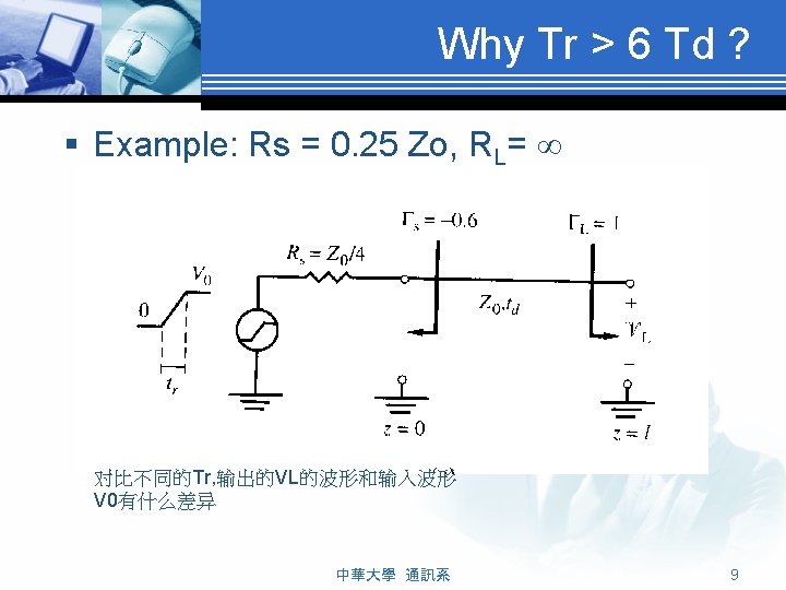

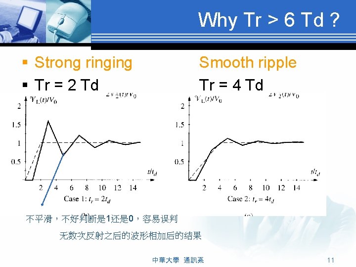
Why Tr > 6 Td ? § Multi-reflections occurred at load § Tr = 2 Td Tr = 4 Td 中華大學 通訊系 10

Example of High-Speed IC Interconnection § § CMOS On-chip 1 mm interconnection Vp= 0. 5 c = 150 mm/ns Td=1 mm/Vp = 0. 067 ns Rule of Thumb only worked as: Tr > 6 Td= 0. 04 ns -1 = 3 GHz FCLK < (8 Tr) § Inductance extraction now is very important !! F《3 G,IC内部 1 mm的连接线可以做为一个Lumped元件 中華大學 通訊系 12

Example of High-Speed IC Interconnection § § 10 mm interconnection between IC’s Vp= 0. 6 c =180 mm/ns Td= 10 mm/Vp = 0. 056 ns Rule of Thumb only worked as: Tr > 6 Td= 0. 33 ns -1 = 375 MHz FCLK < (8 Tr) § Distributed analysis now is very important !! § IC和IC之间 1 cm的连接线,在FCLK < 375 MHz时才可以视为一个Lumped 元件 中華大學 通訊系 13

Sinusoidal EM Wave § Oscillations in Time 中華大學 通訊系 14

Sinusoidal EM Wave § Wave Motion in Space 中華大學 通訊系 15
 §")
Period v. s. Travel Time § Period T = 1/freq Td= L/(freq* ) § VBB’(t) is different from VAA’(t) 中華大學 通訊系 16

Period v. s. Travel Time § 類比 程師的 Rule of thumb § Signal path can be treated as: A lumped element, if Td < T/100 § (Short ckt, series resistor, shunt capacitor) A lumped model, if T/100 < Td < T/20 § (Series inductor with shunt capacitor) A distributed model, if Td > T/20 § (Transmission Line or multi-section LC model) 中華大學 通訊系 17

Trace v. s. Wavelength § 類比 程師的 Rule of thumb § Signal path can be treated as: A lumped element, if L < /100 § (Short ckt, series resistor, shunt capacitor) A lumped model(LC电路), if /100 < L < /20 § (Series inductor with shunt capacitor) A distributed model, if L > /20 § (Transmission Line or multi-section LC model) § 每 1/20 波长LC电路(A lumped model)来表示 中華大學 通訊系 18

Example of Radio-Frequency Interconnection § § For 1 GHz RF signal in PCB circuits Vp= 0. 6 c =180 mm/ns = Vp/freq =180 mm Rule of Thumb only worked as: Td < T/100 = 0. 01 ns L < /100 = 1. 8 mm = 71 mil § Distributed analysis is needed for RF PCB design !! 中華大學 通訊系 19
 Input current")
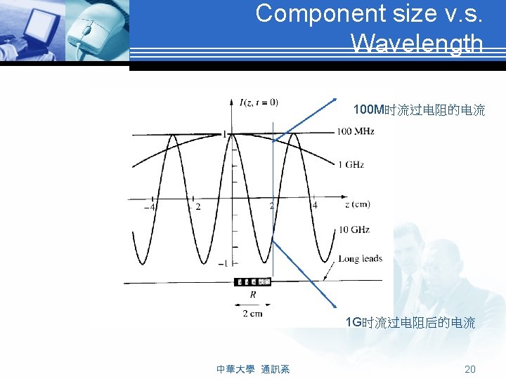
Component size v. s. Wavelength § Definitions of lumped element § (1) Input current amplitude = Output current amplitude § (2) Input current phase = Output current phase § Only at 100 MHz, 2 cm resistor can be treated as a lumped resistor ! 中華大學 通訊系 21
")
Basic Lumped Elements § Resistor Capacitor Inductor § Definitions of lumped element § (1) Input current amplitude = Output current amplitude § (2) Input current phase = Output current phase 中華大學 通訊系 23
 t= 0 -, Vc=0 (a) t=")
Capacitor Time domain : Ic= C (d. Vc/dt) t= 0 -, Vc=0 (a) t= 0+, Vc can be finite value? Ic= infinity !! impossible!!@# (b) t=0+, Vc= 0, Short circuit for instant( 接通瞬间, 电压为 0) (c) Ballastor for impulse voltage Frequency domain : ic= jw. C vc 中華大學 通訊系 24
 t= 0 -, IL=0 (a) t=")
Inductor Time domain : VL= L (d. IL/dt) t= 0 -, IL=0 (a) t= 0+, IL can be finite value? VL = infinity !! impossible!!@# (b) t=0+, IL= 0, Open circuit for instant(接通瞬 间,电流为 0) (c) Ballastor for impulse current(为突然的脉冲电 流做稳流作用,电流不会突变) Frequency domain : v. L= jw. L i. L 中華大學 通訊系 25
 Capacitive")
Practical Capacitor RS C LS With Parasitic Resistor Rs and Inductor Ls(有寄生电感 和寄生电阻) Capacitive |ZC| Inductive 共振频率(可以做 bypass电容) Freq (log) 中華大學 通訊系 26

Practical Inductor RP CP L |YC| With Parasitic Resistor Rp and Capacitor Cp Inductive Capacitive Freq (log) 可以做RF chock,此时阻抗最大 中華大學 通訊系 27

Murata Chip L/C Library 中華大學 通訊系 28

Murata Chip L/C Library 中華大學 通訊系 29
 Due to conductor loss")
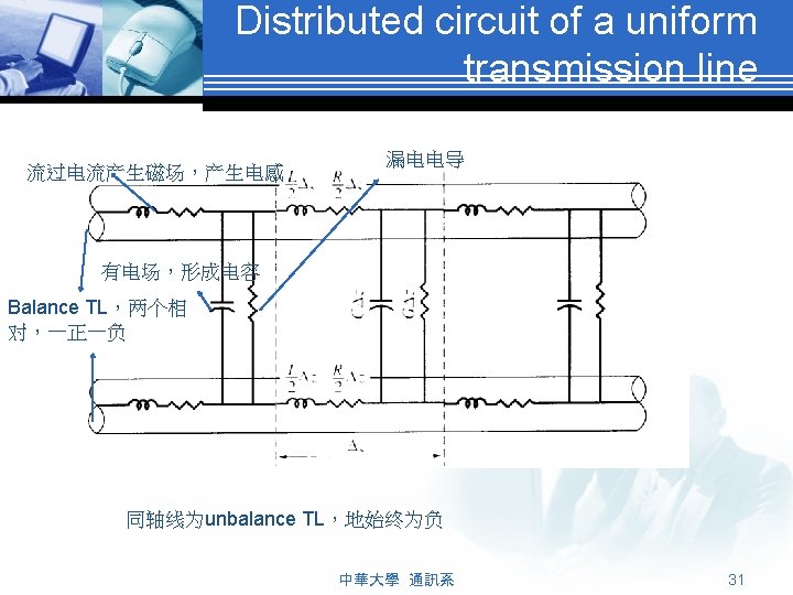
Transmission Line Parameters § R: Resistance per unit length (W/m) Due to conductor loss § L: Inductance per unit length (H/m) § C: Capacitance per unit length (F/m) § G: Conductance per unit length (S/m) Due to dielectric loss 中華大學 通訊系 32

Lumped circuit models for a short segment of a TL 中華大學 通訊系 33

Transmission Line Equations 中華大學 通訊系 34

Transmission Line Equations § Kirchhoff’s voltage law 中華大學 通訊系 35

Transmission Line Equations § Kirchhoff’s current law 中華大學 通訊系 36

Wave Equations for Lossless Line § For a lossless line, R= 0 and G= 0 中華大學 通訊系 37

Traveling-Wave solutions § V+: voltage wave traveling in +z direction § V-: voltage wave traveling in -z direction 中華大學 通訊系 38

Traveling-Wave solutions 中華大學 通訊系 39

Characteristic Impedance 中華大學 通訊系 40

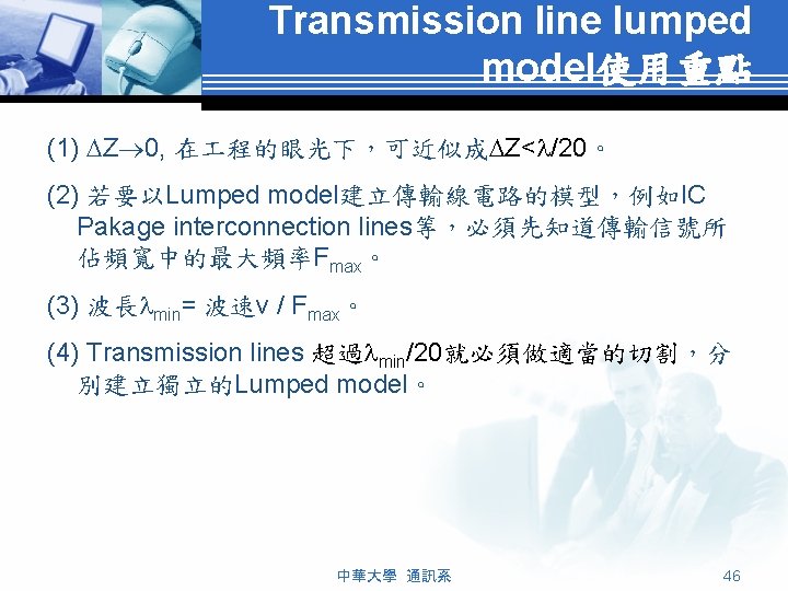
Transmission line lumped model如何正確使用? 中華大學 通訊系 41

Using PSPICE to simulate 100 MHz sinusoidal wave propagating in 40 cm RG -58/U coaxial cable by lumped model. RG-58/U cable Z 0=50 v= 2 x 10⁸ m/s Ideal Line L= 250 n. H/m C= 100 p. F/m =2 m @100 MHz l= 40 cm=0. 2 @100 MHz Delay= 2 ns
 Time delay=2. 55 ns (27.")
Time delay=3. 2 ns (60% Error, Too bad !) Time delay=2. 55 ns (27. 5% Error, Not good !)
 It’s well.")
Time delay=2. 25 ns (12. 5% Error) It’s well.
 It’s good enough!!")
Time delay=2. 11 ns (5. 5% Error) It’s good enough!!

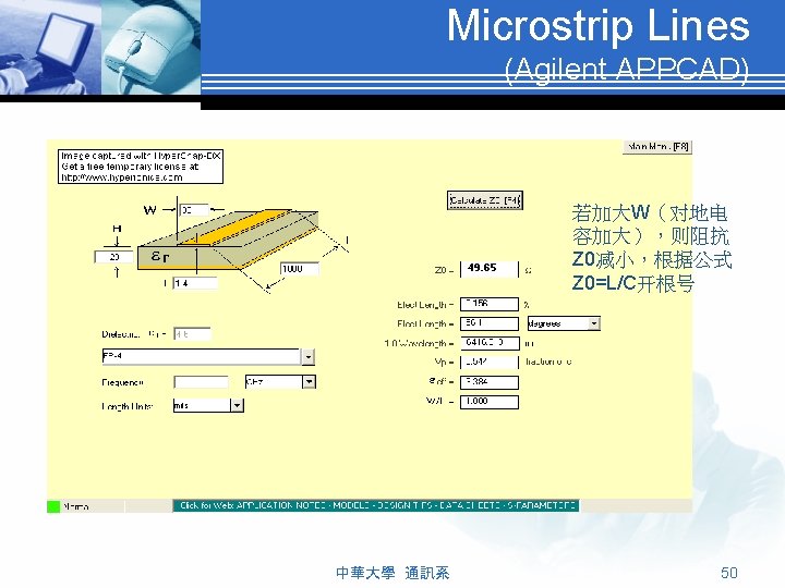
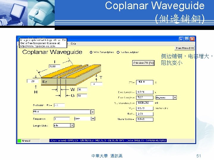
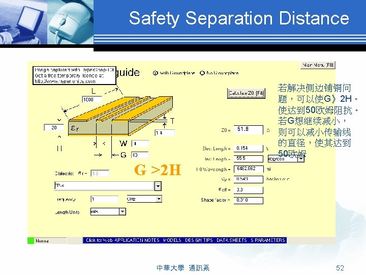
Cross-sectional View of common uniform TL 中華大學 通訊系 47

Transmission Line Parameters 中華大學 通訊系 48

Skin Effect § For low frequency s A § For high frequency Skin depth d s d 高频时,频率越高,截面积越小,阻抗越大 中華大學 通訊系 49
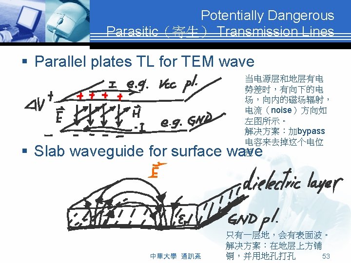
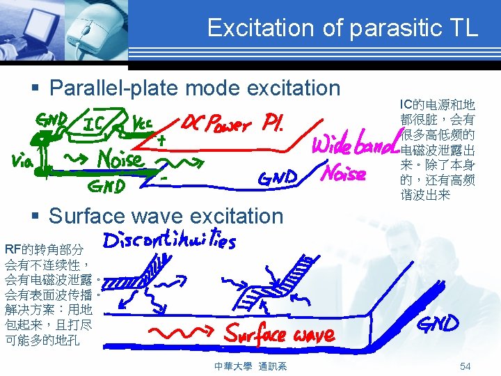
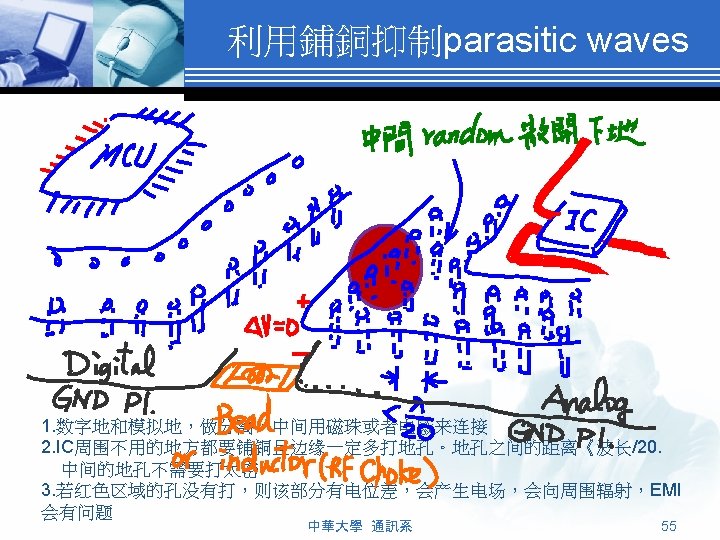
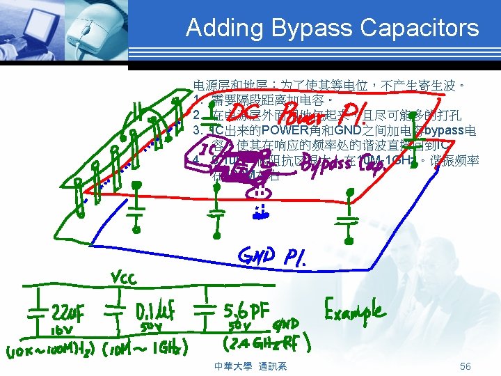
- Slides: 56