Transistor Scaling Integrated Circuit Technology mtinkerutdallas edu EE

- Slides: 35

Transistor Scaling Integrated Circuit Technology mtinker@utdallas. edu EE 4330 Spring Semester

Transistor Scaling Relevant References “Planar Process, ” https: //en. wikipedia. org/wiki/Planar_process 2. “Fairchild’s Approach: The Planar Process, ” https: //www. computerhistory. org/revolution/digitallogic/12/329. 3. “ 1959: Invention of the ‘Planar’ Manufacturing Process, ” https: //www. computerhistory. org/siliconengine/invention-of-the -planar-manufacturing-process/. 4. “ 1959: Practical Monolithic Integrated Circuit Process Patented, ” https: //www. computerhistory. org/siliconengine/practicalmonolithic-integrated-circuit-concept-patented/. 5. “ 1960: First Planar Integrated Circuit Is Fabricated, ” https: //www. computerhistory. org/siliconengine/first-planarintegrated-circuit-is-fabricated/. Integrated Circuit Technology mtinker@utdallas. edu EE 4330 Spring Semester 1.

Transistor Scaling 6. 7. 8. 9. 10. G. E. Moore, “The Role of Fairchild in Silicon Technology in the Early Days of ‘Silicon Valley, ’” Proceedings of the IEEE, Vol. 86, No. 1, pp. 53 -62, 1998. B. Lojek, “History of Semiconductor Engineering, ” Springer, 2007. G. E. Moore, “Cramming More Components onto Integrated Circuits, ’” Electronics, Vol. 38, No. 8, April 19, pp. 114 -117, 1965. G. E. Moore, “Progress in Digital Integrated Electronics, ” International Electron Devices Meeting, pp. 11 -13, 1975. G. E. Moore (2006), ‘Moore’s Law at 40, ’ in D. C. Brock, (ed. ) Understanding Moore’s Law. Philadelphia: Chemical Heritage Press, pp. 67 -84. Integrated Circuit Technology mtinker@utdallas. edu EE 4330 Spring Semester

Transistor Scaling 11. 12. 13. 14. 15. 16. International Technology Roadmap for Semiconductors, 2011 and 2015 Editions. “Moore’s Law, ” https: //en. wikipedia. org/wiki/Moore_law. S. Wolf, “Silicon Processing for the VLSI Era, ” Lattice Press, 2002. IC Knowledge LLC, “Forecasting the 450 mm Ramp Up, ” www. icknowledge. com/news/Forecasting the 450 mm Ramp Up. pdf. A. Holst, “Semiconductor Market Size Worldwide from 1987 to 2020, ” https: //www. statista. com/statistics/266973/global -semiconductor-sales-since-1988/. M. Osborne, “Semiconductor Process Nodes No Longer, ” http: //www. fabtech. org/news/_a/semiconductor_process_nodes _no_longer/. Integrated Circuit Technology mtinker@utdallas. edu EE 4330 Spring Semester

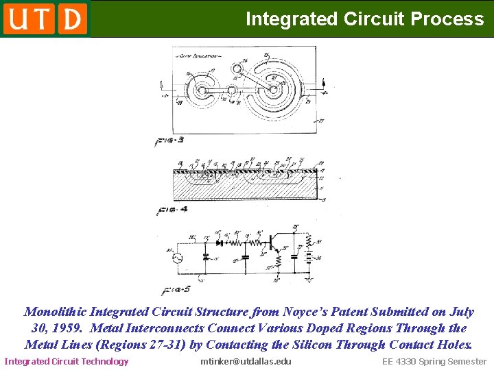
Integrated Circuit Process • Process Technology Enabling the Integrated Circuit Was Invented by Fairchild Semiconductor in 1959 Ø Jean Hoerni from Fairchild Invented the Planar Process Upon Which the Integrated Circuit Is Based in Early 1959 Ø Building Upon this Process Robert Noyce from Fairchild Then Invented the Concept of the Monolithic Integrated Circuit by Connecting Aluminum Metallization Between the Circuit Contacts by Running the Aluminum Wires Over the Planar Oxide Formed on the Silicon Surface Ø Robert Noyce Also Suggested Reverse Biasing Diffused Junctions to Isolate the Electrical Devices Ø Noyce Filed His Patent for this Process in July 1959 Ø Fairchild Ultimately Developed Working Integrated Circuits Based Upon this Process Technology by September 27, 1960 Integrated Circuit Technology mtinker@utdallas. edu EE 4330 Spring Semester

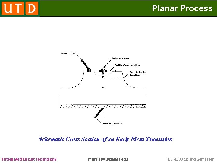
Planar Process • Interestingly, the Planar Process Upon Which the Whole Semiconductor Industry Is Based Was Not Invented to Enable the Integrated Circuit Ø This Process Was Invented to Overcome the Tapping Problem Then Being Seen in the Mesa Transistors Then Being Used to Manufacture Discrete Transistors Ø The Base-Collector Region of These Transistors Was Recessed to Isolate These Devices but the High Electric Fields at the Exposed Junction Was Sensitive to Contamination Ø The Thin Silicon Dioxide Layer on the Surface Was Also Removed Since Conventional Wisdom Considered this Oxide Harmful to the Device Ø Particles Falling Down on this Region from the Packaging Could Cause the Junction to Short Destroying the Device Ø This Problem Could Be Induced by Vigorously Tapping the Packaging Containing the Device with a Pencil to Help Diagnose the Problem Integrated Circuit Technology mtinker@utdallas. edu EE 4330 Spring Semester

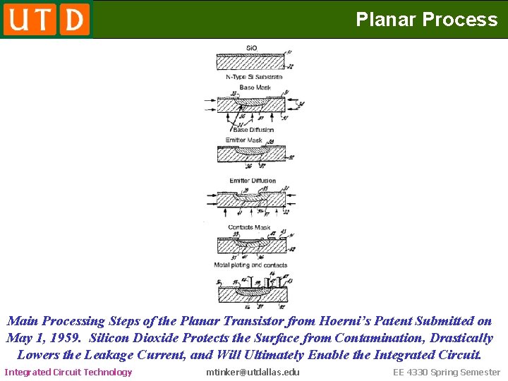
Planar Process • The Planar Process Developed by Hoerni Addressed this Problem Ø Atalla from Bell Labs Determined that Silicon Dioxide Could Passivate the Silicon Surface Drastically Lowering the Surface States and Improving the Quality of the Devices Formed in Silicon Ø This Could Substantially Reduce the Amount of Reverse Bias Leakage in These Devices and Increase the Breakdown Voltage Ø Hoerni Used this Basic Concept to Passivate the Oxide Surface and Then Used the Oxide as a Mask to Form the Diffused Regions of the Transistor and to Later Form Metal Contacts to the Silicon Through Holes Formed in the Oxide in Order to Form Discrete Transistors Ø This Addressed the Tapping Problem, Substantially Improved the Leakage and Breakdown Characteristics of the Devices, and Provided the Basic Process Required to Develop the Monolithic Integrated Circuit Technology mtinker@utdallas. edu EE 4330 Spring Semester

Planar Process Schematic Cross Section of an Early Mesa Transistor. Integrated Circuit Technology mtinker@utdallas. edu EE 4330 Spring Semester

Planar Process Main Processing Steps of the Planar Transistor from Hoerni’s Patent Submitted on May 1, 1959. Silicon Dioxide Protects the Surface from Contamination, Drastically Lowers the Leakage Current, and Will Ultimately Enable the Integrated Circuit Technology mtinker@utdallas. edu EE 4330 Spring Semester

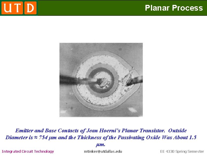
Planar Process Emitter and Base Contacts of Jean Hoerni’s Planar Transistor. Outside Diameter is ≈ 754 µm and the Thickness of the Passivating Oxide Was About 1. 5 μm. Integrated Circuit Technology mtinker@utdallas. edu EE 4330 Spring Semester

Integrated Circuit Process • • The Process for the Integrated Circuit Soon Followed This Process Enabled Devices to Be Shrunk to Extremely Small Dimensions and Revolutionized the Semiconductor Industry Integrated Circuit Technology mtinker@utdallas. edu EE 4330 Spring Semester

Integrated Circuit Process Monolithic Integrated Circuit Structure from Noyce’s Patent Submitted on July 30, 1959. Metal Interconnects Connect Various Doped Regions Through the Metal Lines (Regions 27 -31) by Contacting the Silicon Through Contact Holes. Integrated Circuit Technology mtinker@utdallas. edu EE 4330 Spring Semester

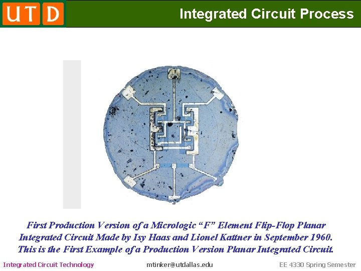
Integrated Circuit Process First Production Version of a Micrologic “F” Element Flip-Flop Planar Integrated Circuit Made by Isy Haas and Lionel Kattner in September 1960. This is the First Example of a Production Version Planar Integrated Circuit Technology mtinker@utdallas. edu EE 4330 Spring Semester

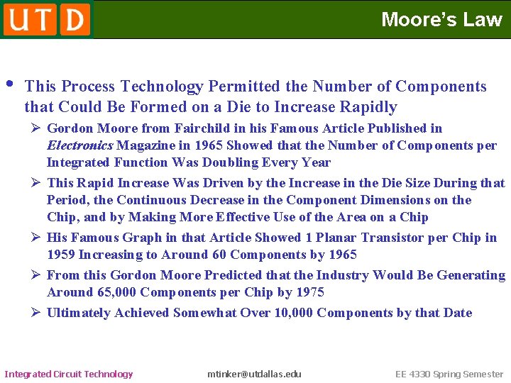
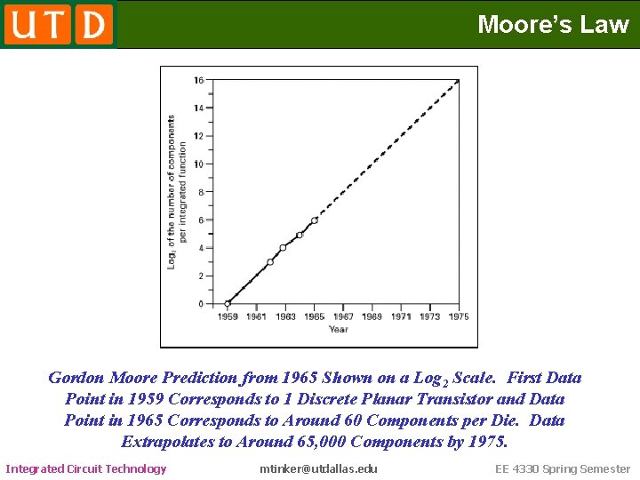
Moore’s Law • This Process Technology Permitted the Number of Components that Could Be Formed on a Die to Increase Rapidly Ø Gordon Moore from Fairchild in his Famous Article Published in Electronics Magazine in 1965 Showed that the Number of Components per Integrated Function Was Doubling Every Year Ø This Rapid Increase Was Driven by the Increase in the Die Size During that Period, the Continuous Decrease in the Component Dimensions on the Chip, and by Making More Effective Use of the Area on a Chip Ø His Famous Graph in that Article Showed 1 Planar Transistor per Chip in 1959 Increasing to Around 60 Components by 1965 Ø From this Gordon Moore Predicted that the Industry Would Be Generating Around 65, 000 Components per Chip by 1975 Ø Ultimately Achieved Somewhat Over 10, 000 Components by that Date Integrated Circuit Technology mtinker@utdallas. edu EE 4330 Spring Semester

Moore’s Law Gordon Moore Prediction from 1965 Shown on a Log 2 Scale. First Data Point in 1959 Corresponds to 1 Discrete Planar Transistor and Data Point in 1965 Corresponds to Around 60 Components per Die. Data Extrapolates to Around 65, 000 Components by 1975. Integrated Circuit Technology mtinker@utdallas. edu EE 4330 Spring Semester

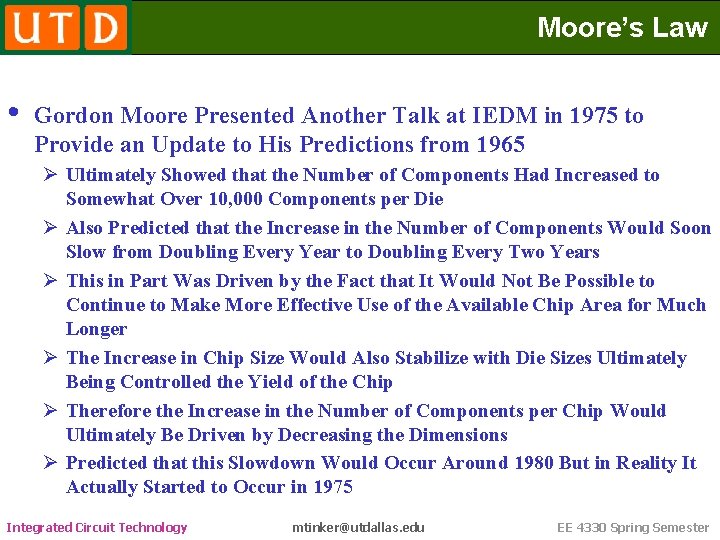
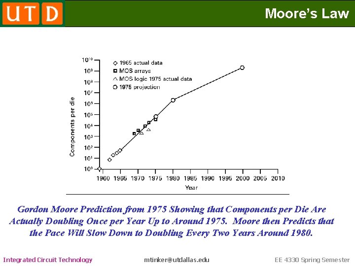
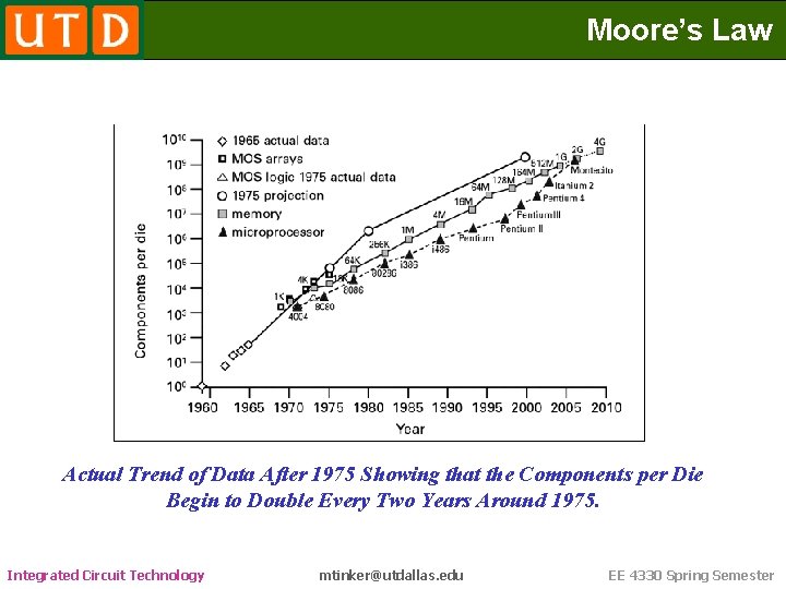
Moore’s Law • Gordon Moore Presented Another Talk at IEDM in 1975 to Provide an Update to His Predictions from 1965 Ø Ultimately Showed that the Number of Components Had Increased to Somewhat Over 10, 000 Components per Die Ø Also Predicted that the Increase in the Number of Components Would Soon Slow from Doubling Every Year to Doubling Every Two Years Ø This in Part Was Driven by the Fact that It Would Not Be Possible to Continue to Make More Effective Use of the Available Chip Area for Much Longer Ø The Increase in Chip Size Would Also Stabilize with Die Sizes Ultimately Being Controlled the Yield of the Chip Ø Therefore the Increase in the Number of Components per Chip Would Ultimately Be Driven by Decreasing the Dimensions Ø Predicted that this Slowdown Would Occur Around 1980 But in Reality It Actually Started to Occur in 1975 Integrated Circuit Technology mtinker@utdallas. edu EE 4330 Spring Semester

Moore’s Law Gordon Moore Prediction from 1975 Showing that Components per Die Are Actually Doubling Once per Year Up to Around 1975. Moore then Predicts that the Pace Will Slow Down to Doubling Every Two Years Around 1980. Integrated Circuit Technology mtinker@utdallas. edu EE 4330 Spring Semester

Moore’s Law Actual Trend of Data After 1975 Showing that the Components per Die Begin to Double Every Two Years Around 1975. Integrated Circuit Technology mtinker@utdallas. edu EE 4330 Spring Semester

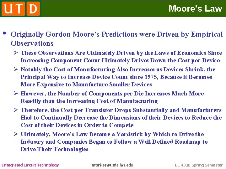
Moore’s Law • Originally Gordon Moore’s Predictions were Driven by Empirical Observations Ø These Observations Are Ultimately Driven by the Laws of Economics Since Increasing Component Count Ultimately Drives Down the Cost per Device Ø Notably the Cost of Manufacturing Also Increases as Devices Shrink, the Principal Way to Increase Device Count since 1975, Because it Becomes More Expensive to Manufacture Smaller Devices Ø However, the Number of Components per Die Increases Much More Readily than the Increasing Cost of Manufacturing Ø Therefore, the Cost per Transistor Drops Substantially and Manufacturers Had to Continually Decrease the Dimensions of their Devices to Reduce the Cost of their Devices in Order to Compete Ø Ultimately, Moore’s Law Became a Yardstick by Which to Drive the Industry and Companies Began to Follow a Well Defined Roadmap to Drive Their Technologies Integrated Circuit Technology mtinker@utdallas. edu EE 4330 Spring Semester

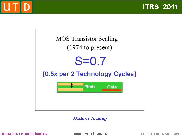
ITRS 2011 Historic Scaling Integrated Circuit Technology mtinker@utdallas. edu EE 4330 Spring Semester

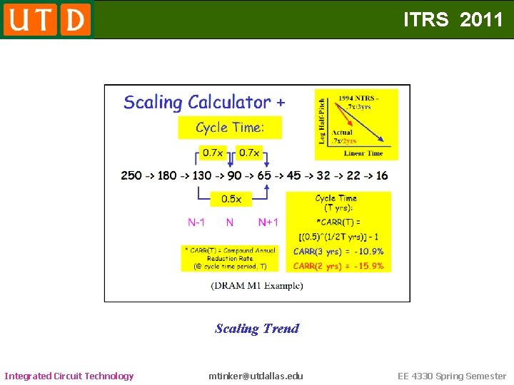
ITRS 2011 Scaling Trend Integrated Circuit Technology mtinker@utdallas. edu EE 4330 Spring Semester

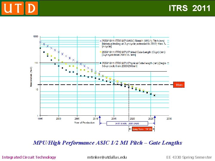
ITRS 2011 MPU/High Performance ASIC 1/2 M 1 Pitch – Gate Lengths Integrated Circuit Technology mtinker@utdallas. edu EE 4330 Spring Semester

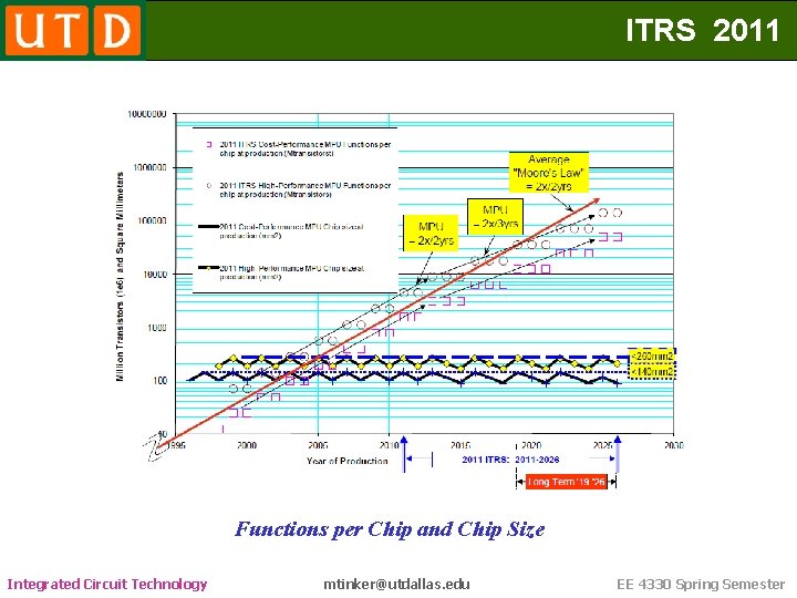
ITRS 2011 Functions per Chip and Chip Size Integrated Circuit Technology mtinker@utdallas. edu EE 4330 Spring Semester

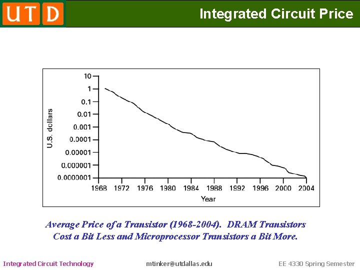
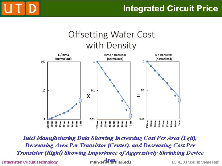
Integrated Circuit Price • • This Has Led to a Precipitous Drop in the Price of a Transistor These Drops in Price Have Continued Even Until Today Down to the 10 nm Technology Node Integrated Circuit Technology mtinker@utdallas. edu EE 4330 Spring Semester

Integrated Circuit Price Average Price of a Transistor (1968 -2004). DRAM Transistors Cost a Bit Less and Microprocessor Transistors a Bit More. Integrated Circuit Technology mtinker@utdallas. edu EE 4330 Spring Semester

Integrated Circuit Price Intel Manufacturing Data Showing Increasing Cost Per Area (Left), Decreasing Area Per Transistor (Center), and Decreasing Cost Per Transistor (Right) Showing Importance of Aggressively Shrinking Device Area. Integrated Circuit Technology mtinker@utdallas. edu EE 4330 Spring Semester

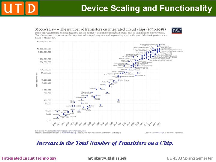
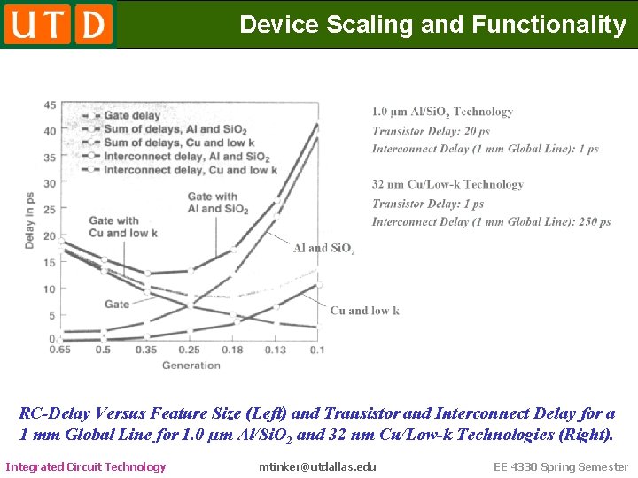
Device Scaling and Functionality • This Decrease in the Transistor Size Has Had Two Other Distinct Benefits Ø This Has Increased the Total Functionality of the Chip Generating Chips with Far Greater Processing Power Ø Device Scaling Has Also Substantially Increased the Speed of the Transistors from Around 2 MHz in 1975 to 3 GHz in 2002 Although Speed Increases Have Largely Stopped Since 2002 Because of Interconnect Delays Integrated Circuit Technology mtinker@utdallas. edu EE 4330 Spring Semester

Device Scaling and Functionality Increase in the Total Number of Transistors on a Chip. Integrated Circuit Technology mtinker@utdallas. edu EE 4330 Spring Semester

Device Scaling and Functionality RC-Delay Versus Feature Size (Left) and Transistor and Interconnect Delay for a 1 mm Global Line for 1. 0 µm Al/Si. O 2 and 32 nm Cu/Low-k Technologies (Right). Integrated Circuit Technology mtinker@utdallas. edu EE 4330 Spring Semester

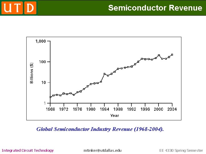
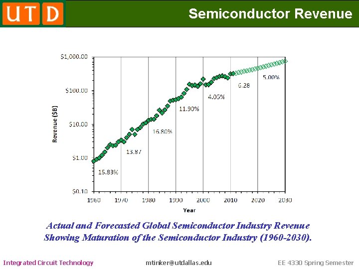
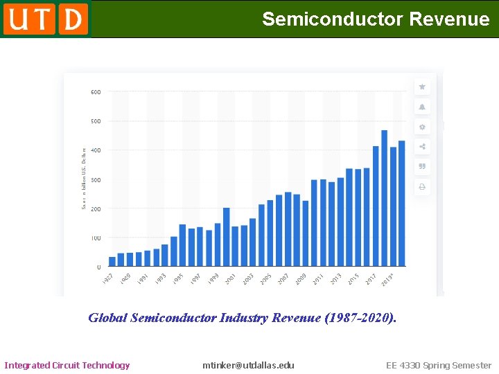
Semiconductor Revenue • These Drops in Price and Increase in Processor Speeds Have Greatly Expanded the Number of Applications for Integrated Circuits Resulting in Substantial Growth in the Semiconductor Industry Integrated Circuit Technology mtinker@utdallas. edu EE 4330 Spring Semester

Semiconductor Revenue Global Semiconductor Industry Revenue (1968 -2004). Integrated Circuit Technology mtinker@utdallas. edu EE 4330 Spring Semester

Semiconductor Revenue Actual and Forecasted Global Semiconductor Industry Revenue Showing Maturation of the Semiconductor Industry (1960 -2030). Integrated Circuit Technology mtinker@utdallas. edu EE 4330 Spring Semester

Semiconductor Revenue Global Semiconductor Industry Revenue (1987 -2020). Integrated Circuit Technology mtinker@utdallas. edu EE 4330 Spring Semester

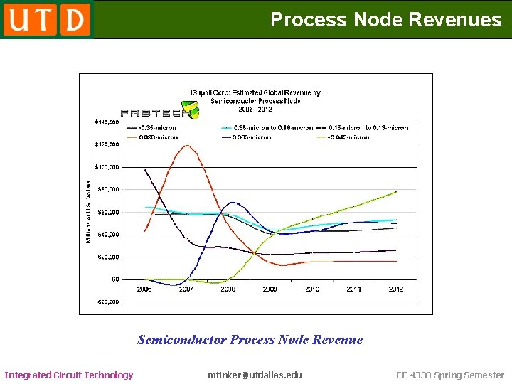
Process Node Revenues • Notably Much of the Industry Continues to Produce Integrated Circuits with Much Larger Dimensions Since These Older Nodes Prove Quite Adequate for Many Applications Integrated Circuit Technology mtinker@utdallas. edu EE 4330 Spring Semester

Process Node Revenues Semiconductor Process Node Revenue Integrated Circuit Technology mtinker@utdallas. edu EE 4330 Spring Semester