Transistor BJT Introduction BJT Bipolar Junction Transistor Vaccum
Transistor (BJT)
Introduction • BJT (Bipolar Junction Transistor) • Vaccum tubes • It comes because it is most advantageous in amplification • Why it is called transistor? Transistor = Transfer + Resistor • Why it is called BJT? • Types of BJT
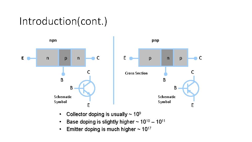
Introduction(cont. ) npn pnp n C C B E p n p C C Cross Section B B B Schematic Symbol E • Collector doping is usually ~ 109 • Base doping is slightly higher ~ 1010 – 1011 • Emitter doping is much higher ~ 1017 E
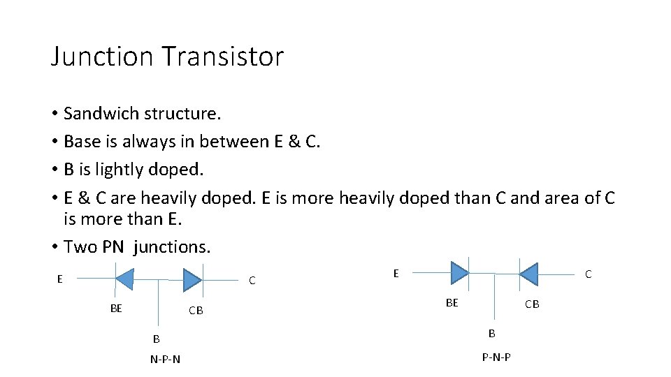
Junction Transistor • Sandwich structure. • Base is always in between E & C. • B is lightly doped. • E & C are heavily doped. E is more heavily doped than C and area of C is more than E. • Two PN junctions. E C BE CB B N-P-N E C BE CB B P-N-P
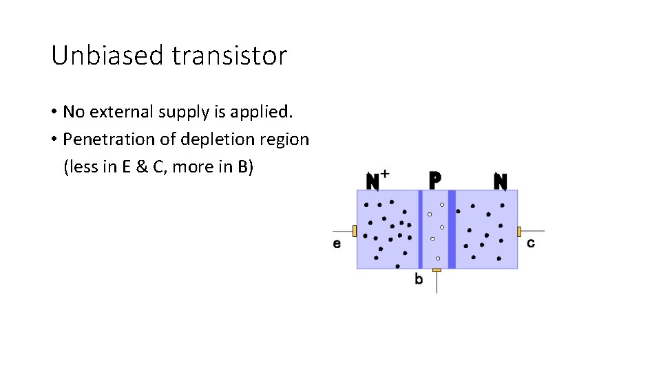
Unbiased transistor • No external supply is applied. • Penetration of depletion region (less in E & C, more in B)
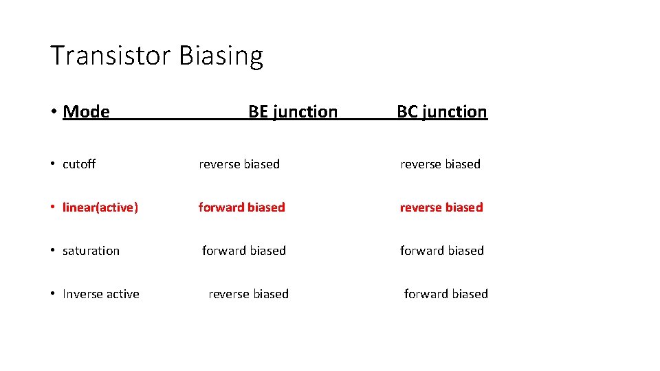
Transistor Biasing • Mode BE junction BC junction • cutoff reverse biased • linear(active) forward biased reverse biased • saturation forward biased • Inverse active reverse biased forward biased
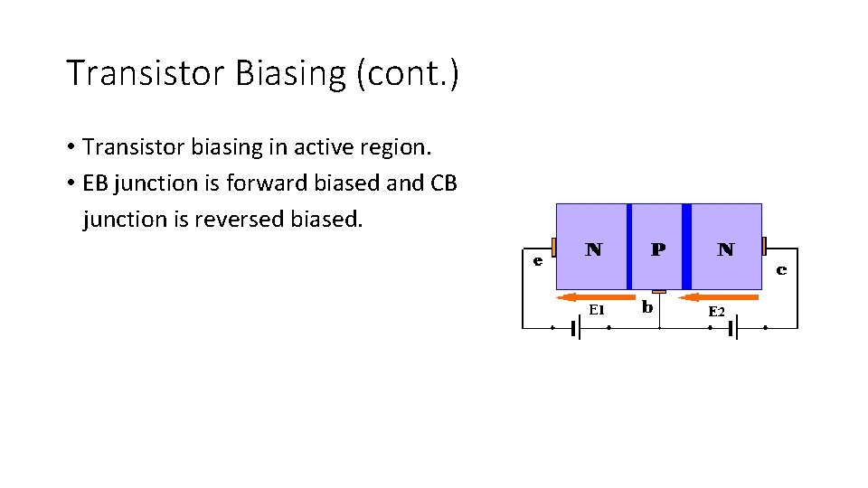
Transistor Biasing (cont. ) • Transistor biasing in active region. • EB junction is forward biased and CB junction is reversed biased.
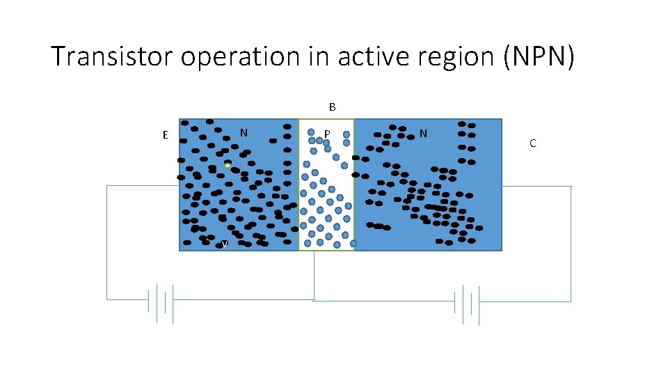
Transistor operation in active region (NPN) B N E v P N C
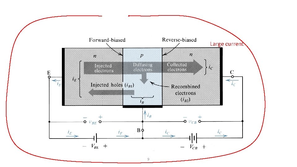
Large current 9
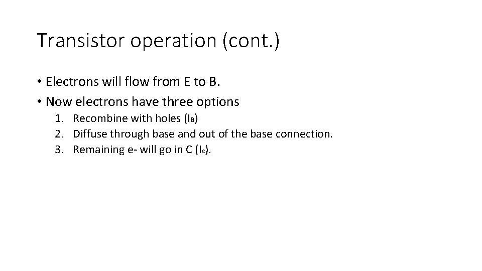
Transistor operation (cont. ) • Electrons will flow from E to B. • Now electrons have three options 1. Recombine with holes (IB) 2. Diffuse through base and out of the base connection. 3. Remaining e- will go in C (Ic).

Transistor operation (cont. ) IE=IB+IC B E Emitter current N Electrons emitted Recombination current P N Electrons collected C Collector current
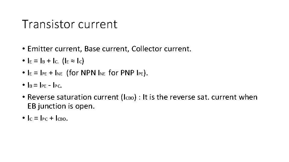
Transistor current • Emitter current, Base current, Collector current. • IE = IB + IC. (IE ≈ IC) • IE = IPE + INE (for NPN INE for PNP IPE). • IB = IPE - IPC. • Reverse saturation current (ICBO) : It is the reverse sat. current when EB junction is open. • IC = IPC + ICBO.
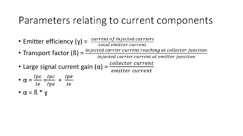
Parameters relating to current components •

Transistor as an amplifier Discussion of an amplification effect With E. g. for common-base configuration transistor:
Transistor construction technologies • Grown type. • Alloy type. • Electrochemically etched type. • Diffusion type • Epitaxial type.
Transistor configuration • Made one of three terminal common to i/p and o/p. • Depending on which terminal is made common. There are three possibilities 1. Common base configuration (CB). 2. Common emitter configuration (CE). 3. Common collector configuration (CC).
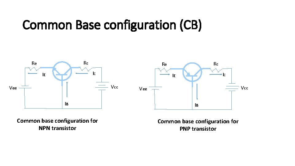
Common Base configuration (CB) Rc Re IC IE Rc Re Vcc Vee IB Common base configuration for NPN transistor IC IE Vcc Vee IB Common base configuration for PNP transistor
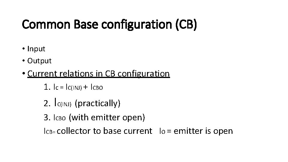
Common Base configuration (CB) • Input • Output • Current relations in CB configuration 1. Ic = IC(INJ) + ICBO 2. IC(INJ) (practically) 3. ICBO (with emitter open) ICB= collector to base current IO = emitter is open
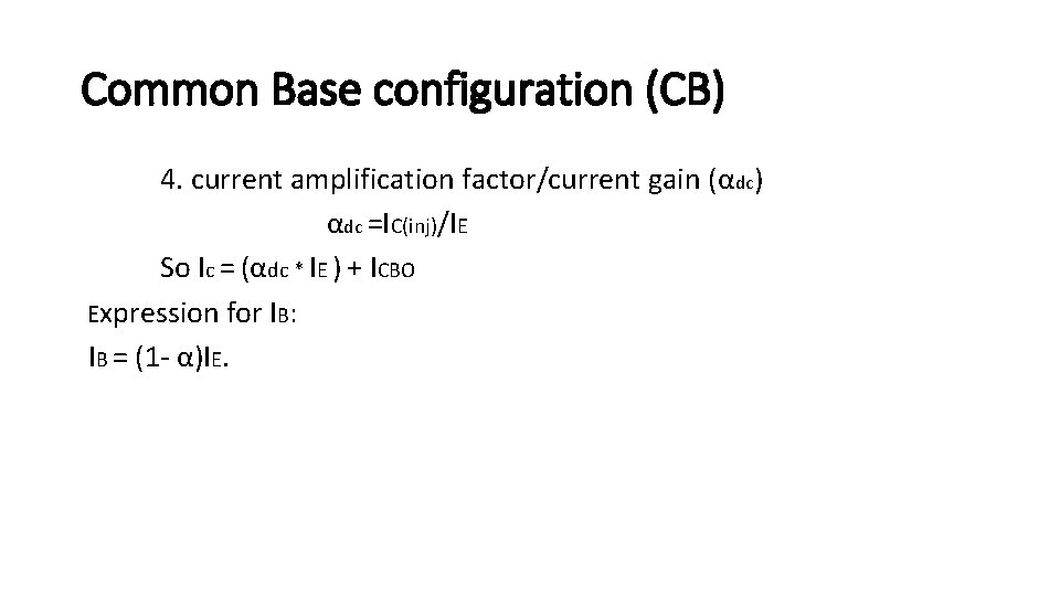
Common Base configuration (CB) 4. current amplification factor/current gain (αdc) αdc =IC(inj)/IE So Ic = (αdc * IE ) + ICBO Expression for IB: IB = (1 - α)IE.
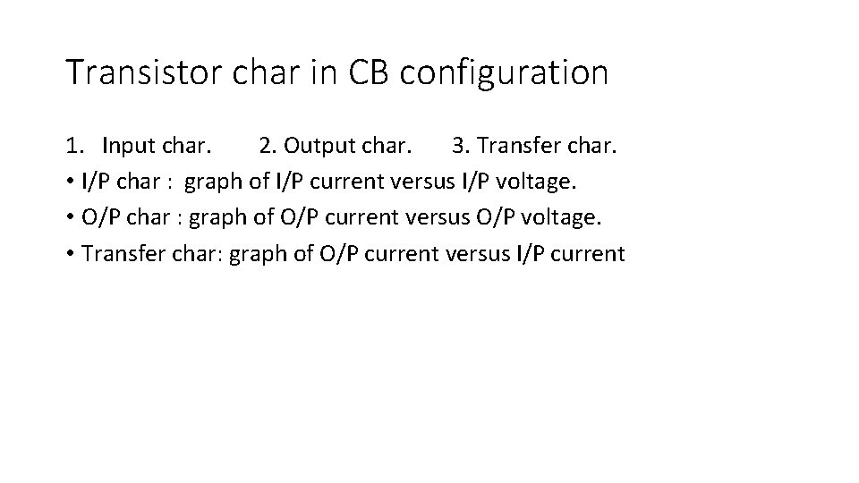
Transistor char in CB configuration 1. Input char. 2. Output char. 3. Transfer char. • I/P char : graph of I/P current versus I/P voltage. • O/P char : graph of O/P current versus O/P voltage. • Transfer char: graph of O/P current versus I/P current
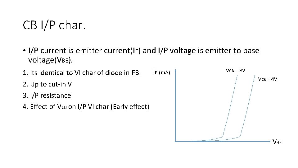
CB I/P char. • I/P current is emitter current(IE) and I/P voltage is emitter to base voltage(VBE). 1. Its identical to VI char of diode in FB. 2. Up to cut-in V 3. I/P resistance 4. Effect of VCB on I/P VI char (Early effect) IE (m. A) VCB = 8 V VCB = 4 V VBE
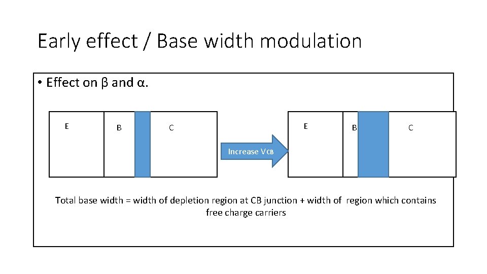
Early effect / Base width modulation • Effect on β and α. E B E C B C Increase VCB Total base width = width of depletion region at CB junction + width of region which contains free charge carriers
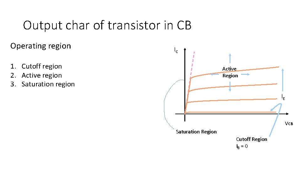
Output char of transistor in CB Operating region IC 1. Cutoff region 2. Active region 3. Saturation region Active Region IE VCB Saturation Region Cutoff Region IB = 0
Output char of transistor in CB • Cut off region : region below the curve IE =0 • Active region : IC ≈ IE (Const. current source) • Dynamic O/P resistance • Saturation region • Current controlled current source.
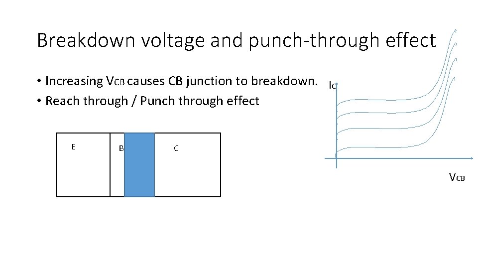
Breakdown voltage and punch-through effect • Increasing VCB causes CB junction to breakdown. IC • Reach through / Punch through effect E B C VCB
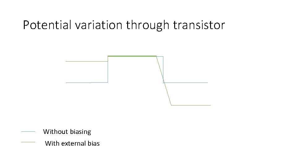
Potential variation through transistor Without biasing With external bias
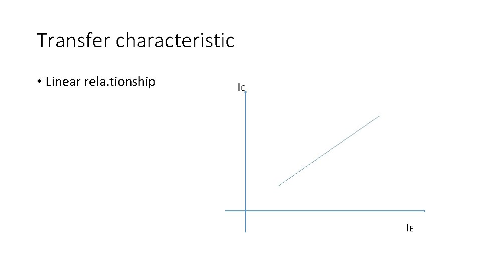
Transfer characteristic • Linear rela. tionship IC IE
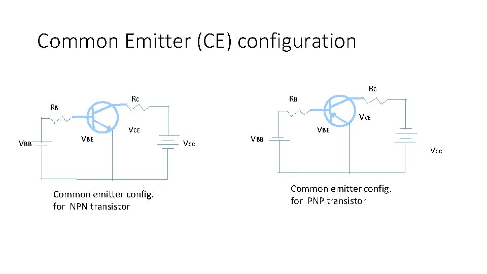
Common Emitter (CE) configuration RC RB VBB RC RB VCE VBE VCE Common emitter config. for NPN transistor Vcc VBB VBE Vcc Common emitter config. for PNP transistor
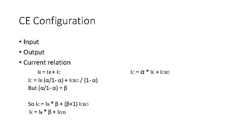
CE Configuration • Input • Output • Current relation IE = IB + IC IC = IB (α/1 - α) + ICBO / (1 - α) But (α/1 - α) = β So IC = IB * β + (β+1) ICBO IC = IB * β + ICEO IC = α * IE + ICBO
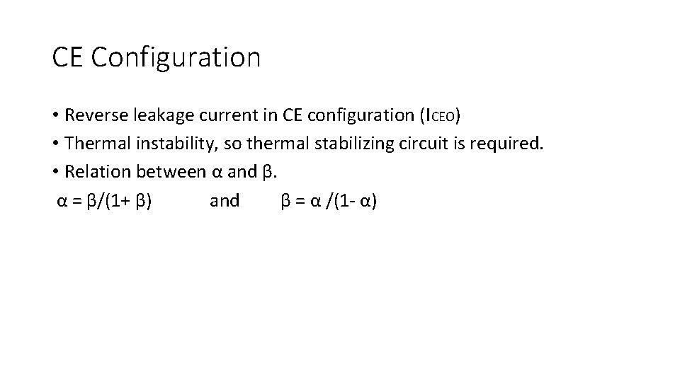
CE Configuration • Reverse leakage current in CE configuration (ICEO) • Thermal instability, so thermal stabilizing circuit is required. • Relation between α and β. α = β/(1+ β) and β = α /(1 - α)
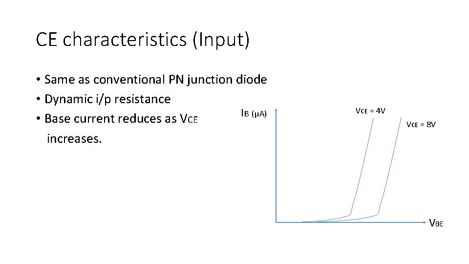
CE characteristics (Input) • Same as conventional PN junction diode • Dynamic i/p resistance IB (μA) • Base current reduces as VCE increases. VCE = 4 V VCE = 8 V VBE

CE characteristics (output) 1. Cut off region 2. Active region 3. Saturation region 4. Dynamic O/P resistance 5. Definition of β 6. Maximum VCE and breakdown
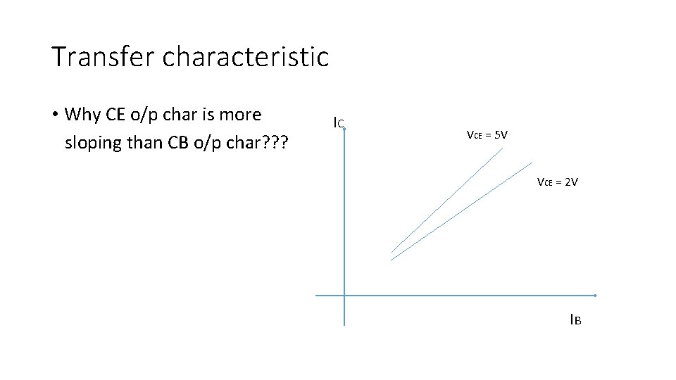
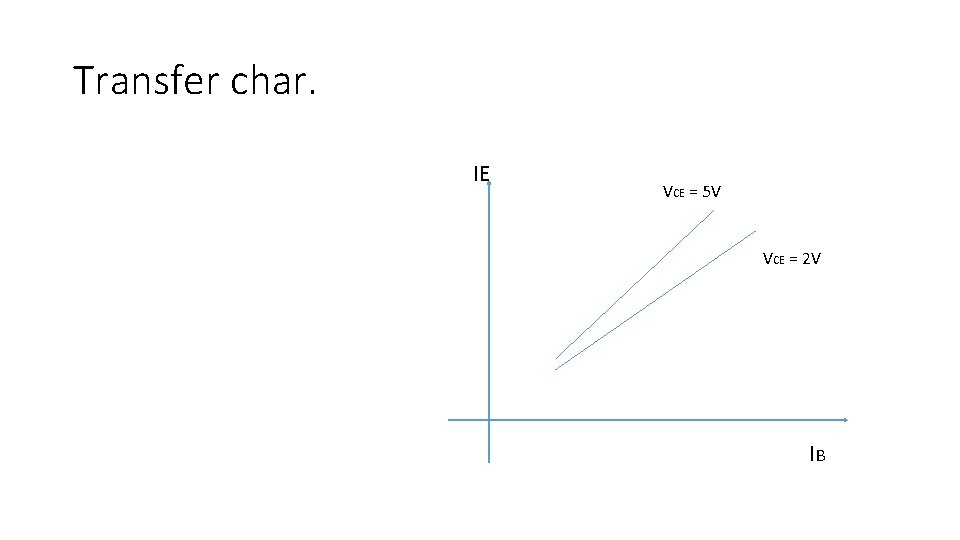
Transfer characteristic • Why CE o/p char is more sloping than CB o/p char? ? ? IC VCE = 5 V VCE = 2 V IB
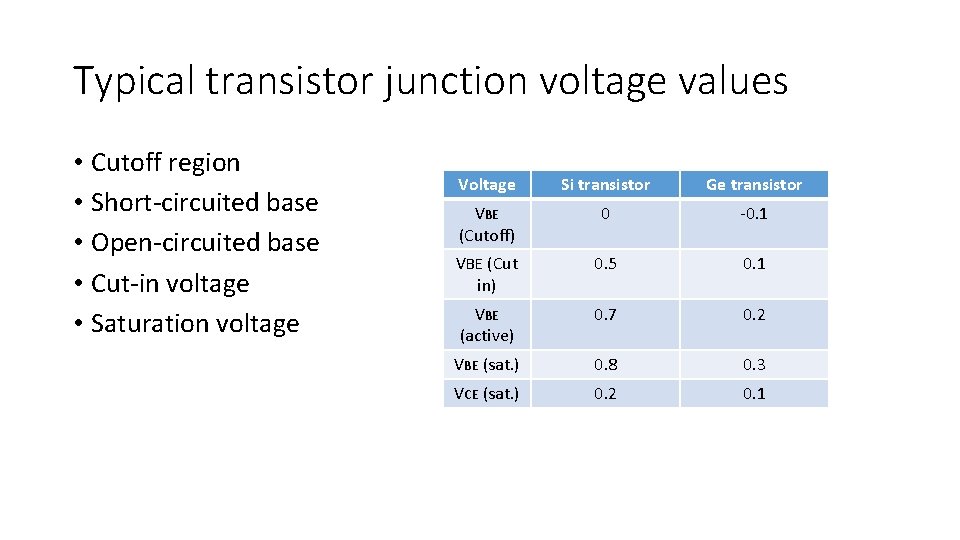
Typical transistor junction voltage values • Cutoff region • Short-circuited base • Open-circuited base • Cut-in voltage • Saturation voltage Voltage Si transistor Ge transistor VBE (Cutoff) 0 -0. 1 VBE (Cut in) 0. 5 0. 1 VBE (active) 0. 7 0. 2 VBE (sat. ) 0. 8 0. 3 VCE (sat. ) 0. 2 0. 1
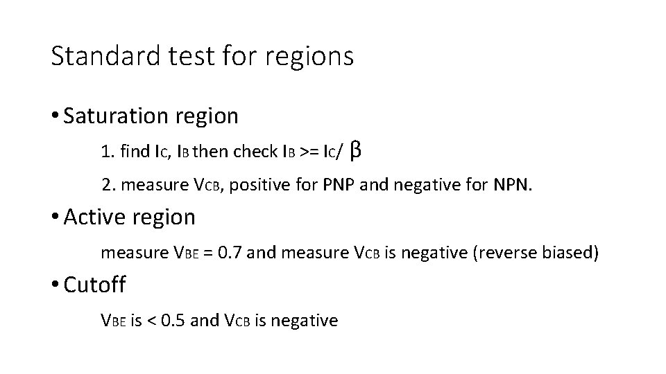
Standard test for regions • Saturation region 1. find IC, IB then check IB >= IC/ β 2. measure VCB, positive for PNP and negative for NPN. • Active region measure VBE = 0. 7 and measure VCB is negative (reverse biased) • Cutoff VBE is < 0. 5 and VCB is negative
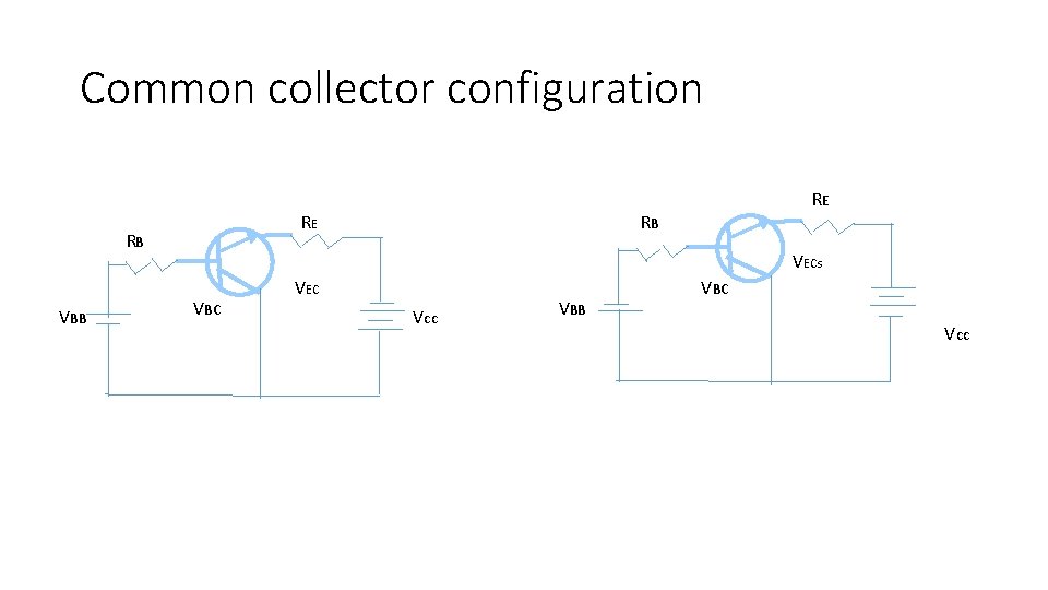
Common collector configuration RE RB VBB RE RB VECs VBC VEC Vcc VBB VBC Vcc
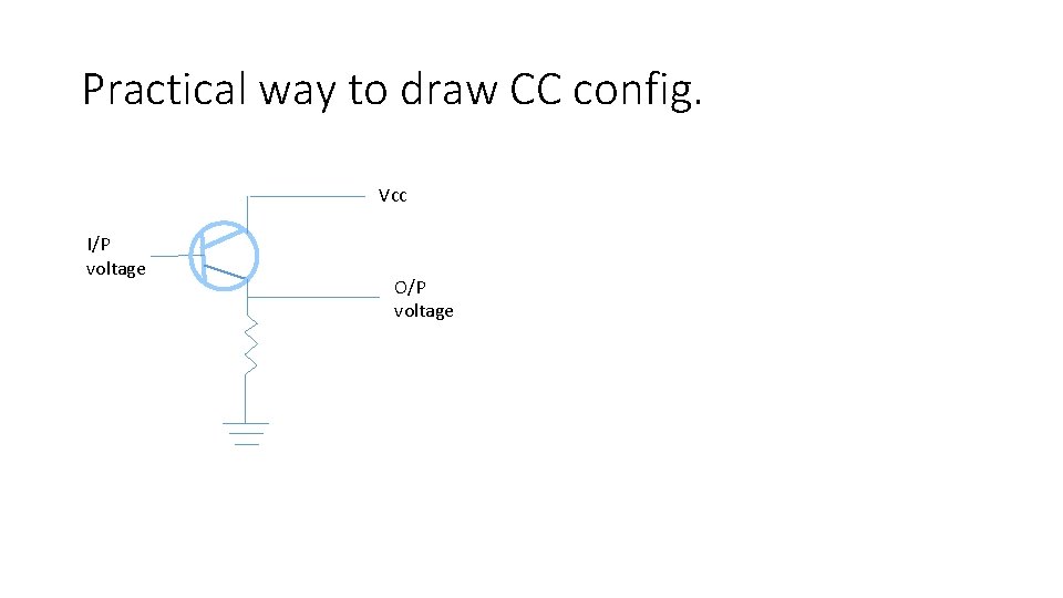
Practical way to draw CC config. VCC I/P voltage O/P voltage
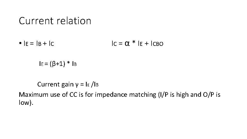
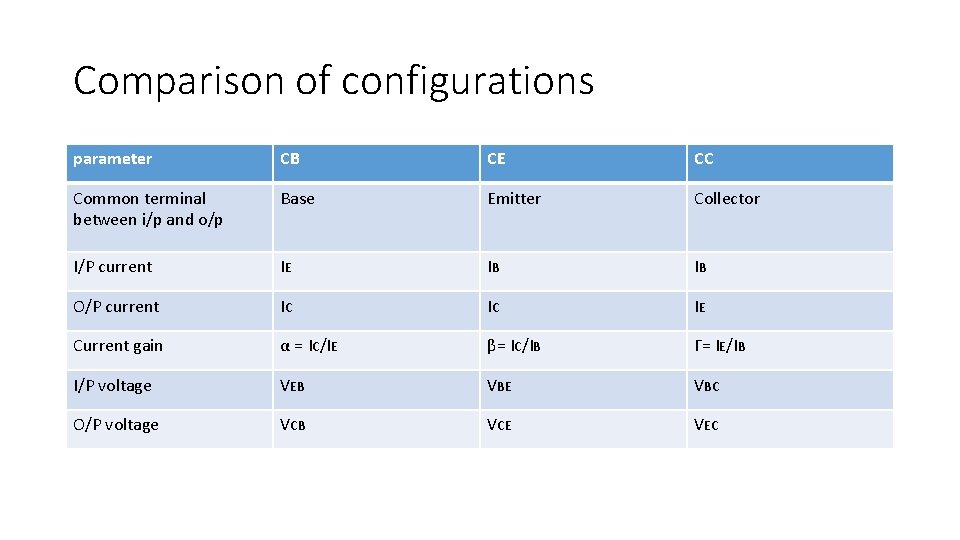
Current relation • IE = IB + IC IC = α * IE + ICBO IE = (β+1) * IB Current gain γ = IE /IB Maximum use of CC is for impedance matching (I/P is high and O/P is low).
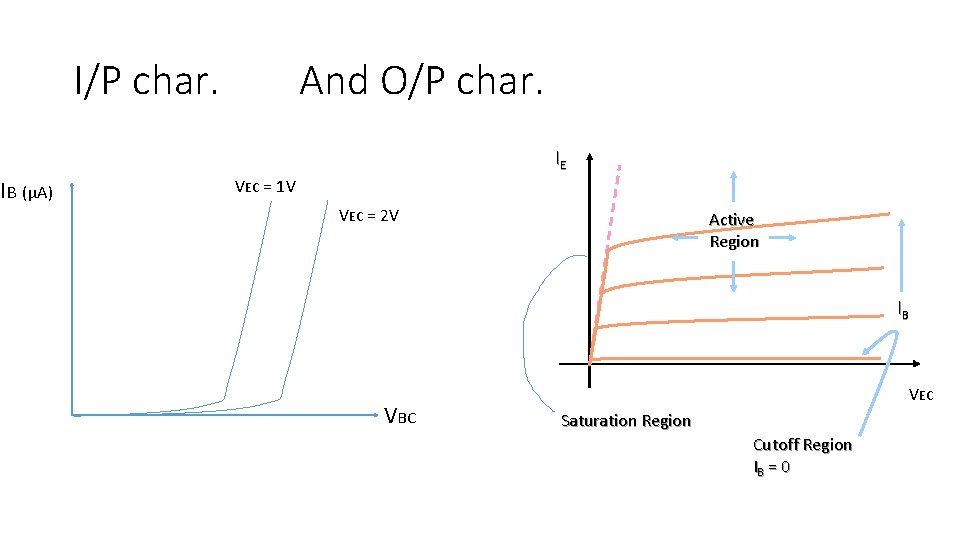
IB (μA) I/P char. And O/P char. IE VEC = 1 V VEC = 2 V Active Region IB VBC VEC Saturation Region Cutoff Region IB = 0
Transfer char. IE VCE = 5 V VCE = 2 V IB
Comparison of configurations parameter CB CE CC Common terminal between i/p and o/p Base Emitter Collector I/P current IE IB IB O/P current IC IC IE Current gain α = IC/IE β= IC/IB Γ= IE/IB I/P voltage VEB VBE VBC O/P voltage VCB VCE VEC
Analytic expression for transistor char. •
Base spreading resistance VCE E C VE VC VCB VEB B VCB = VC + rbb * IB
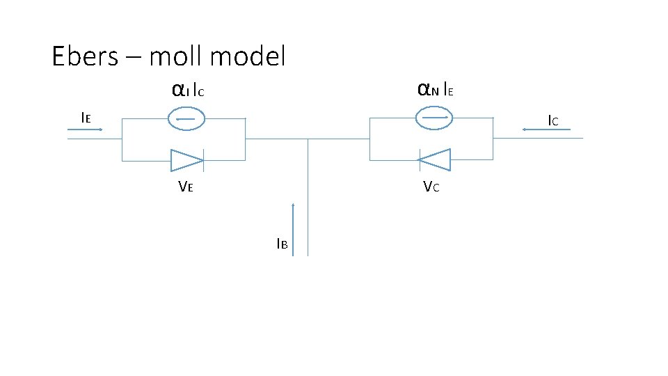
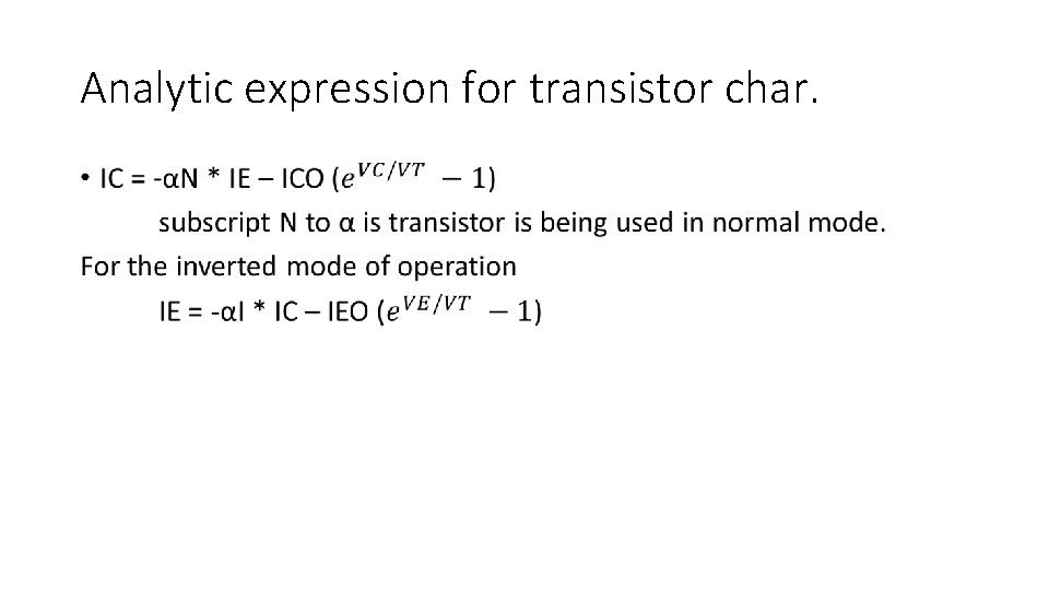
Ebers – moll model αI I C αN I E IE IC VE VC IB
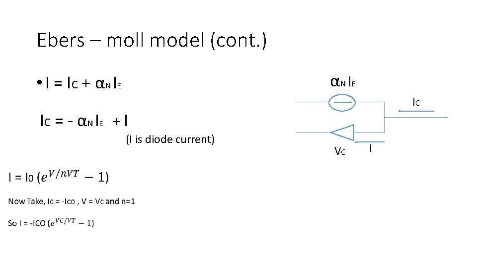
Ebers – moll model (cont. ) αN I E • I = I C + αN I E IC I C = - αN I E + I (I is diode current) VC I
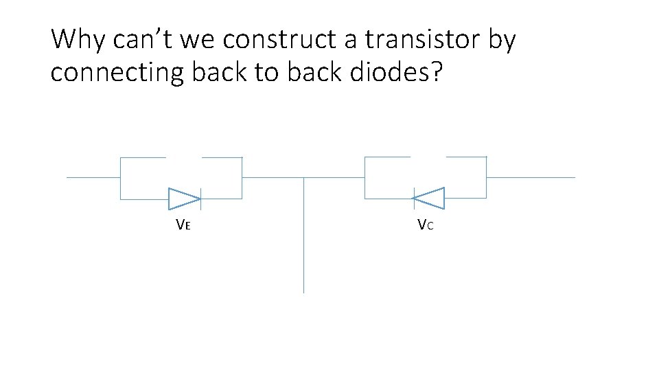
Why can’t we construct a transistor by connecting back to back diodes? VE VC
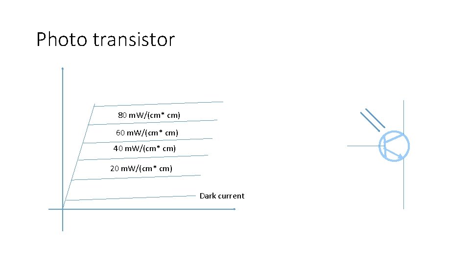
Photo transistor 80 m. W/(cm* cm) 60 m. W/(cm* cm) 40 m. W/(cm* cm) 20 m. W/(cm* cm) Dark current
Photo transistor (cont. ) • Advantages: • Photo current multiplied by β • High sensitivity • Good switching speed • No memory effect.
Phototransistor (cont. ) • Disadvantages • Not so fast as conventional transistor because of photoconducting material • Poor linearity • Temperature sensitive device • External voltage source is needed for operation
- Slides: 49