transform your ideas into products High Speed PCB

transform your ideas into products High Speed PCB Design ㈜ 에이로직스 성남시 분당구 서현동 250 -2 한빛은행 B/D 4층 4층 전화 : 031 -703 -5006 팩스 : 031 -781 -5006 031 -703 -5006 031 -781 -5006 www. alogics. co. kr 1

Agenda transform your ideas into products • High-speed PCB란? – Critical length • High-Speed PCB설계를 위한 기본 지식 – 임피던스 매칭의 필요성 – 적층구조, Termination 결정 • High-speed PCB설계 Guide – 3 -W Rule, 20 -H Rule – 설계 Guide • High-speed PCB 설계 사례 – IMT 2000, ATM 및 기타 적용사례 2

Today’s Technologies transform your ideas into products • Faster Rise Times & Lower Noise Margins 3

Propagation Delay transform your ideas into products • Tpd of Electromagnetic fields in various media Medium Air (radio waves) Coax cable (75% velocity) Coax cable (66% velocity) FR 4 PCB, outer trace FR 4 PCB, inner trace Alumina PCB, inner trace Delay ps/in 85 113 129 140 -180 240 -270 Dielectric Constant 1. 0 1. 8 2. 3 2. 8 -4. 5 8. 0 -10. 0 4

High-Speed PCB? transform your ideas into products • PCB에서의 패턴길이가 Critical Length보다 크면 Transmission Line 해석을 해야 한다 Effective Length • Critical Length = L 7 = Vpd x Tr 7 C = er Tr 7 • When C = 3 x 10⁸ m/s, Tr = 1 ns, er = 4. 5 Then Critical Length = 20 mm 5

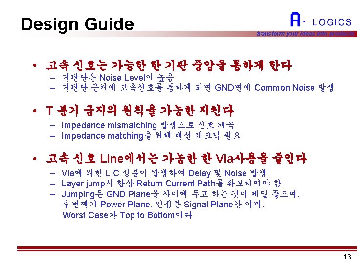
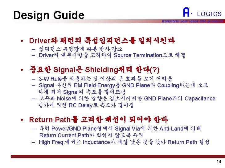
Impedance Matching Γ= transform your ideas into products RL - Zo RL + Zo • RL = Zo 일때 Reflection이 발생하지 않는다 • 적층구조는 대칭구조로 한다(Layer 및 Gap) • Termination 방법 및 저항 값을 결정 – Source Termination – End Termination 6

Characteristic Impedance transform your ideas into products • Microstrip Line 절연체두께 W T ZO = h 5. 98 h 87 ln 0. 8 W + T er + 1. 414 유전율 패턴굵기 도체두께 • Strip Line W T h B ZO = 1. 9 B 60 ln 0. 8 W + T er 7

Termination transform your ideas into products • Series Termination S RS Zo L – RS = Z O - R d – DC Noise Margin 좋음 – RS 저항은 Source단에 가깝게 • Parallel Termination S Zo L – RL = Z O – Power 소모가 문제 – RL 저항은 Load단에서 분기 RL 8

Termination transform your ideas into products • RC Termination S Zo L RL CL – RL = ZO , CL = 300 p. F – 2 Parts 추가 – Band Width 고려 CL 값 결정 • Thevenin Termination VCC S Zo RL RL L – RL = 2 ZO – 2 Parts 추가 – High Power for CMOS 9

3 -W Rule Other Trace Clock Trace 3 W transform your ideas into products Other Trace ≥W ≥ 2 W ≥W 3 W Ground Plane 2 W 2 W Differential Pair Trace W • Crosstalk를 최소화하기위해 Trace Width를 W라고할 때 Center to Center를 3 W이상 이격(70% Flux Boundary) – For 98% Flux Boundary, use 10 -W Rule • Differential Pair Trace는 위의 그림 참조 • Board Edge부분과는 충분히 거리를 둔다 10

20 -H Rule transform your ideas into products RF H 20 H H H 20 H • High speed PCB에서 Power Plane Edge에서 RF Current 발생함. 이를 Fringing이라고 함 – Magnetic Flux Linkage에 의해 발생함 • 이를 최소화 하기위해 Power Plane은 가장 가까운 Ground Plane보다 두 층간 Gap을 H라고 할 때 20 H만큼 작게 해 주어야 함 11
, G(1), P(1) 1.")
Layer Stackup transform your ideas into products • 4 Layer S(2), G(1), P(1) 1. S 2. G 3. P 4. S • 1. S : Best layer for flux cancellation • 2~3층간 Gap을 작게하여 Power Impedance를 줄인다. • Poor flux cancellation • 6 Layer S(4), G(1), P(1) 1. S 2. G 3. S 4. S 5. P 6. S • 1. S : Only safe routing layer S(4), G(1), P(1) 1. S 2. S 3. G 4. P 5. S 6. S • 2. S : Good flux cancellation S(3), G(2), P(1) 1. S 2. G 3. S 4. P 5. G 6. S • 1 S, 3 S : Excellent routing layer • 6. S : Good flux cancellation 16

Layer Stackup • 8 Layer • 10 Layer 1. S 2. S 3. G 4. S 5. S 6. P 7. S 8. S 1. S • 2. S, 4 S : Excellent routing Layer S(6), G(1), P(1) 8. S 2. G 3. S 4. S 5. G 6. P 7. S 8. S 9. G 10. S 1. S 2. G 3. S 4. G 5. P 6. S 7. G transform your ideas into products • 1. S, 3 S, 6 S, 8 S : Excellent routing Layer S(6), G(3), P(1) • 1. S, 3 S, 4 S, 8 S, 10 S : Excellent routing Layer • 7 S : Poor flux cancellation S(4), G(3), P(1) 17
- Slides: 17