TPATCT A New Transient Current Technique based on
TPA-TCT A New Transient Current Technique based on the Two. Photon-Absorption process for 3 D high-spatial-resolution characterization of semiconductor radiation sensors EP Detector seminar, CERN, January 26 th, 2018 Iván Vila Álvarez Instituto de Física de Cantabria (CSIC-UC)
Brigade de Cusine M. Fernández, J. González, R. Jaramillo, D. Moya, I. Vila Instituto de Física de Cantabria (CSIC-UC) M. Moll CERN R. Montero Universidad del Pais Vasco (UPV-EHU) F. R. Palomo Universidad de Sevilla (US) Ivan. Vila@csic. es, EP Detector Seminar, January 26 th 2018, CERN 2
Outline — Introduction: _ _ — TPA-TCT Proof-of-concept. _ _ — Non irradiated planar n-in-p pad diode Theoretical model vs. experiment. Application cases: _ _ — Transient Current Techniques for semiconductor radiation sensors characterization. Two-Photo-Absorption basics. Radiation damage on LGAD diodes. High-resolution Mapping of HV-CMOS deep n-well. Outlook: developing turn-key tool. Ivan. Vila@csic. es, EP Detector Seminar, January 26 th 2018, CERN 3
Part 1 - Ingredients: Transient Current Technique & Two-Photon Absorption basics Ivan. Vila@csic. es, EP Detector Seminar, January 26 th 2018, CERN 4
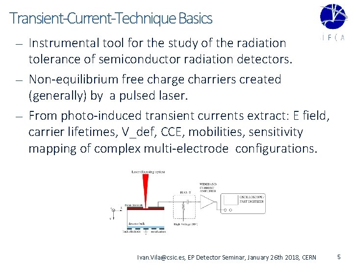
Transient-Current-Technique Basics — — — Instrumental tool for the study of the radiation tolerance of semiconductor radiation detectors. Non-equilibrium free charge charriers created (generally) by a pulsed laser. From photo-induced transient currents extract: E field, carrier lifetimes, V_def, CCE, mobilities, sensitivity mapping of complex multi-electrode configurations. Ivan. Vila@csic. es, EP Detector Seminar, January 26 th 2018, CERN 5
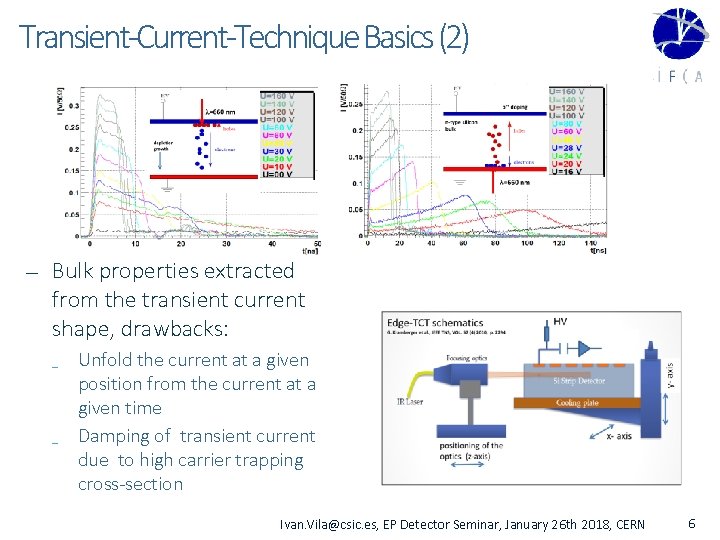
Transient-Current-Technique Basics (2) — Bulk properties extracted from the transient current shape, drawbacks: _ _ Unfold the current at a given position from the current at a given time Damping of transient current due to high carrier trapping cross-section Ivan. Vila@csic. es, EP Detector Seminar, January 26 th 2018, CERN 6
Transient-Current-Technique Basics (3) — Ideally, a TCT technique with non-equilibrium free carriers generation in a very localized volume (micrometric-scale voxel) should allow the best E field mapping and geometry determination of the semiconductor junctions with very small size features of the new generation of position-sensitive-detectors — Let’s see what non-linear optics can do for us… Ivan. Vila@csic. es, EP Detector Seminar, January 26 th 2018, CERN 7
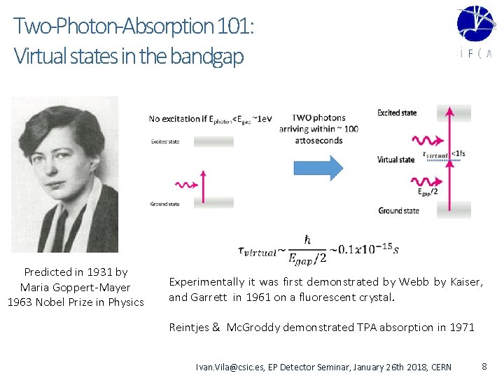
Two-Photon-Absorption 101: Virtual states in the bandgap Predicted in 1931 by Maria Goppert-Mayer 1963 Nobel Prize in Physics Experimentally it was first demonstrated by Webb by Kaiser, and Garrett in 1961 on a fluorescent crystal. Reintjes & Mc. Groddy demonstrated TPA absorption in 1971 Ivan. Vila@csic. es, EP Detector Seminar, January 26 th 2018, CERN 8
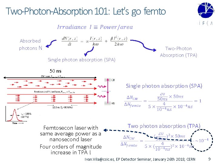
Two-Photon-Absorption 101: Let′s go femto Absorbed photons N Single photon absorption (SPA) Two-Photon Absorption (TPA) 50 ns Single photon absorption (SPA) Femtosecon laser with same average power as a nanosecond laser Four orders of magnitude increase in TPA ! Two photon absorption (TPA) Ivan. Vila@csic. es, EP Detector Seminar, January 26 th 2018, CERN 9
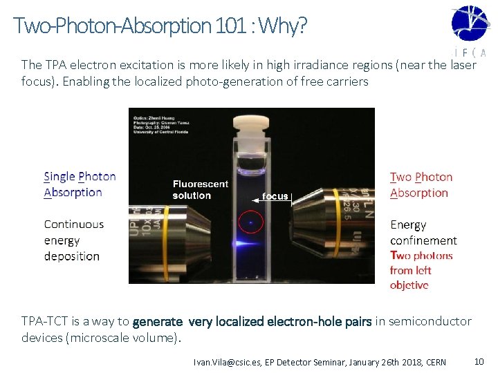
Two-Photon-Absorption 101 : Why? The TPA electron excitation is more likely in high irradiance regions (near the laser focus). Enabling the localized photo-generation of free carriers TPA-TCT is a way to generate very localized electron-hole pairs in semiconductor devices (microscale volume). Ivan. Vila@csic. es, EP Detector Seminar, January 26 th 2018, CERN 10
Part 2 - Cooking the new method. Recipe: Mix TPA & TCT Proof-of-concept on an non-irradiated n -in-p pad diode Ivan. Vila@csic. es, EP Detector Seminar, January 26 th 2018, CERN 11
TPA-TCT Proof-of-concept Challenges 1. 2. 3. Confirm the generation of TPA induced current in a silicon diode with the appropriate laser power. Determine the dimensions of the charge-carrier’s generation volume. Compare the experimental TCT current waveforms against theoretical simulated current waveforms. Ivan. Vila@csic. es, EP Detector Seminar, January 26 th 2018, CERN 12
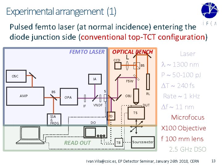
Experimental arrangement (1) Pulsed femto laser (at normal incidence) entering the diode junction side (conventional top-TCT configuration) FEMTO LASER OPTICAL BENCH L CCD BS OSC IA AMP FSW S BS VNDF IF SSA & FROG RL OBJ OPA DUT TS PD DO READ OUT TB Sourcemeter Laser l 1300 nm P 50 -100 p. J DT 240 fs Rate 1 k. Hz Df 11 nm Microfocus X 100 Objective f 100 mm lens 2. 5 GHz DSO Ivan. Vila@csic. es, EP Detector Seminar, January 26 th 2018, CERN 13
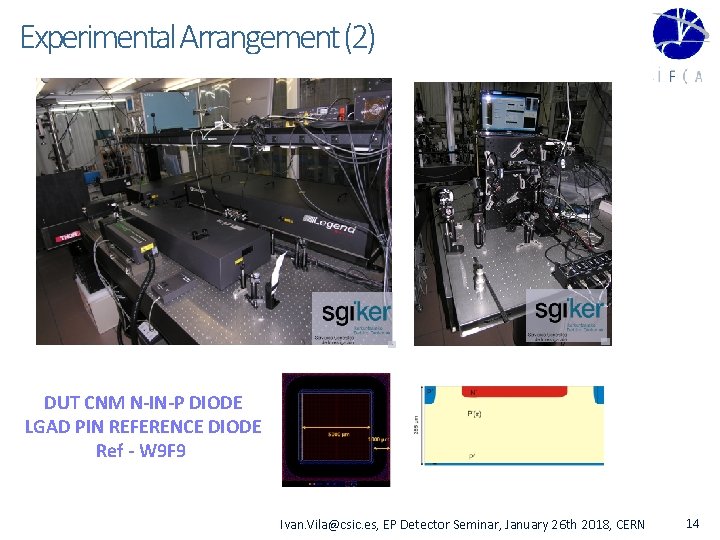
Experimental Arrangement (2) DUT CNM N-IN-P DIODE LGAD PIN REFERENCE DIODE Ref - W 9 F 9 Ivan. Vila@csic. es, EP Detector Seminar, January 26 th 2018, CERN 14
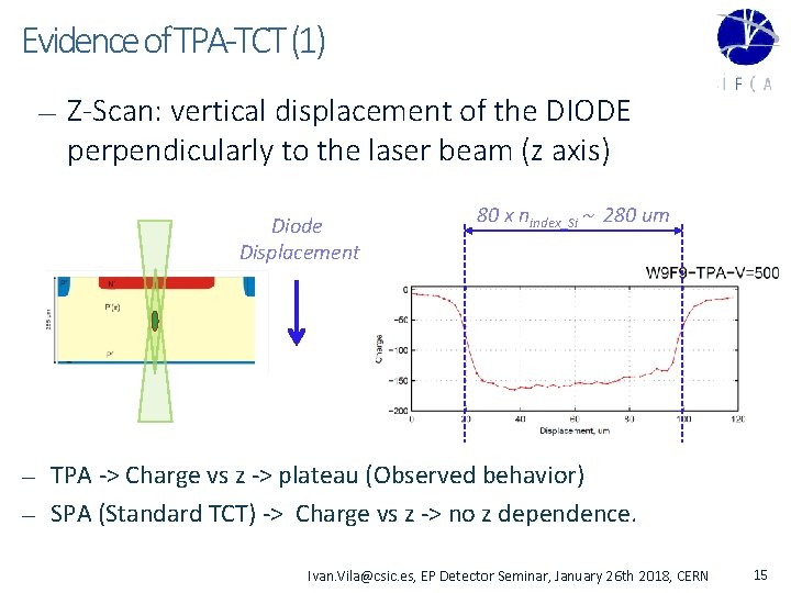
Evidence of TPA-TCT (1) — Z-Scan: vertical displacement of the DIODE perpendicularly to the laser beam (z axis) Diode Displacement — — 80 x nindex_Si 280 um TPA -> Charge vs z -> plateau (Observed behavior) SPA (Standard TCT) -> Charge vs z -> no z dependence. Ivan. Vila@csic. es, EP Detector Seminar, January 26 th 2018, CERN 15
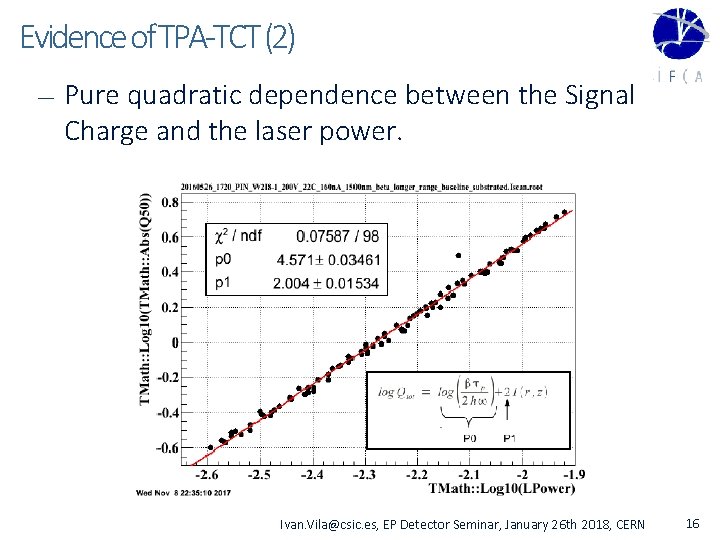
Evidence of TPA-TCT (2) — Pure quadratic dependence between the Signal Charge and the laser power. Ivan. Vila@csic. es, EP Detector Seminar, January 26 th 2018, CERN 16
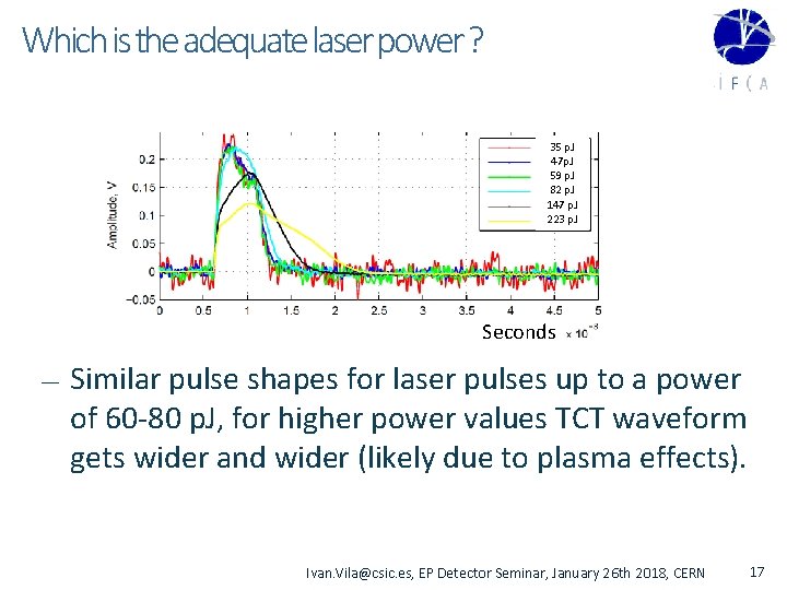
Which is the adequate laser power ? 35 p. J 47 p. J 59 p. J 82 p. J 147 p. J 223 p. J Seconds — Similar pulse shapes for laser pulses up to a power of 60 -80 p. J, for higher power values TCT waveform gets wider and wider (likely due to plasma effects). Ivan. Vila@csic. es, EP Detector Seminar, January 26 th 2018, CERN 17
TPA-TCT Proof-of-concept Challenges 1. 2. 3. Confirm the generation of TPA induced current in a silicon diode with the appropriate laser power. Determine the dimensions of the charge-carrier’s generation volume. Compare the experimental TCT current waveforms against theoretical simulated current waveforms. Ivan. Vila@csic. es, EP Detector Seminar, January 26 th 2018, CERN 18
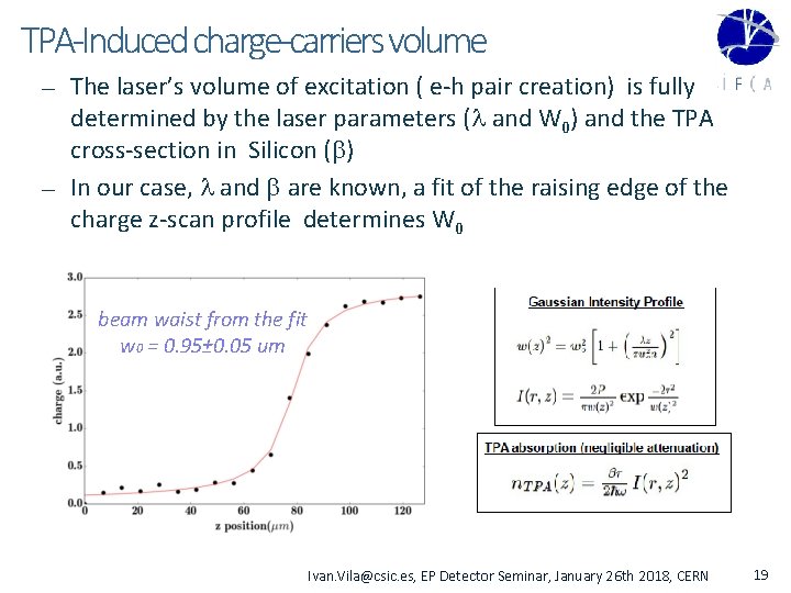
TPA-Induced charge-carriers volume — — The laser’s volume of excitation ( e-h pair creation) is fully determined by the laser parameters (l and W 0) and the TPA cross-section in Silicon (b) In our case, l and b are known, a fit of the raising edge of the charge z-scan profile determines W 0 beam waist from the fit w 0 = 0. 95± 0. 05 um Ivan. Vila@csic. es, EP Detector Seminar, January 26 th 2018, CERN 19
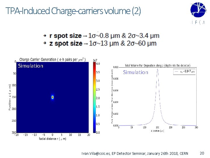
TPA-Induced Charge-carriers volume (2) Simulation Ivan. Vila@csic. es, EP Detector Seminar, January 26 th 2018, CERN 20
TPA-TCT Proof-of-concept Challenges 1. 2. 3. Confirm the generation of TPA induced current in a silicon diode with the appropriate laser power. Determine the dimensions of the charge-carrier’s generation volume. Compare the experimental TCT current waveforms against theoretical simulated current waveforms. Ivan. Vila@csic. es, EP Detector Seminar, January 26 th 2018, CERN 21
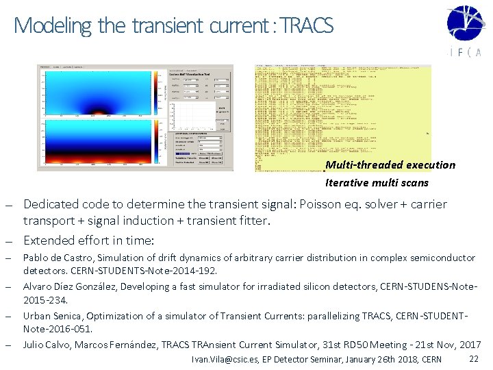
Modeling the transient current : TRACS Multi-threaded execution Iterative multi scans — — — Dedicated code to determine the transient signal: Poisson eq. solver + carrier transport + signal induction + transient fitter. Extended effort in time: Pablo de Castro, Simulation of drift dynamics of arbitrary carrier distribution in complex semiconductor detectors. CERN-STUDENTS-Note-2014 -192. Alvaro Díez González, Developing a fast simulator for irradiated silicon detectors, CERN-STUDENS-Note 2015 -234. Urban Senica, Optimization of a simulator of Transient Currents: parallelizing TRACS, CERN-STUDENTNote-2016 -051. Julio Calvo, Marcos Fernández, TRACS TRAnsient Current Simulator, 31 st RD 50 Meeting - 21 st Nov, 2017 Ivan. Vila@csic. es, EP Detector Seminar, January 26 th 2018, CERN 22
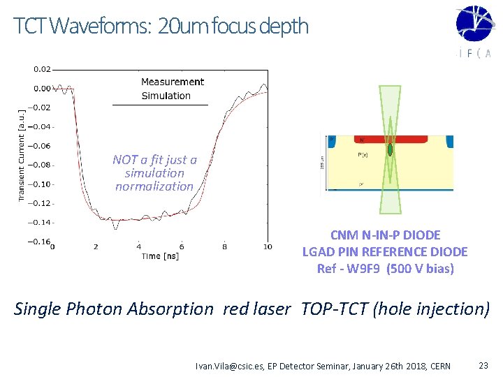
TCT Waveforms: 20 um focus depth NOT a fit just a simulation normalization CNM N-IN-P DIODE LGAD PIN REFERENCE DIODE Ref - W 9 F 9 (500 V bias) Single Photon Absorption red laser TOP-TCT (hole injection) Ivan. Vila@csic. es, EP Detector Seminar, January 26 th 2018, CERN 23
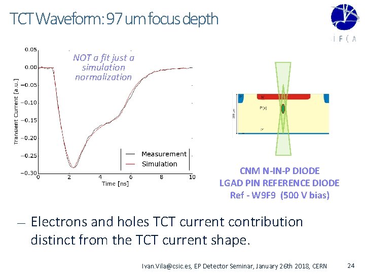
TCT Waveform: 97 um focus depth NOT a fit just a simulation normalization CNM N-IN-P DIODE LGAD PIN REFERENCE DIODE Ref - W 9 F 9 (500 V bias) — Electrons and holes TCT current contribution distinct from the TCT current shape. Ivan. Vila@csic. es, EP Detector Seminar, January 26 th 2018, CERN 24
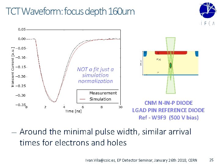
TCT Waveform: focus depth 160 um CNM N-IN-P DIODE LGAD PIN REFERENCE DIODE Ref - W 9 F 9 (500 V bias) — Around the minimal pulse width, similar arrival times for electrons and holes Ivan. Vila@csic. es, EP Detector Seminar, January 26 th 2018, CERN 25
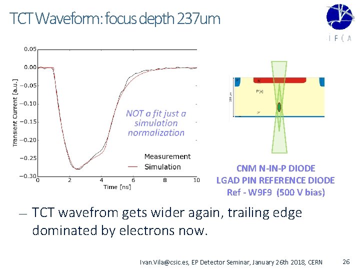
TCT Waveform: focus depth 237 um CNM N-IN-P DIODE LGAD PIN REFERENCE DIODE Ref - W 9 F 9 (500 V bias) — TCT wavefrom gets wider again, trailing edge dominated by electrons now. Ivan. Vila@csic. es, EP Detector Seminar, January 26 th 2018, CERN 26
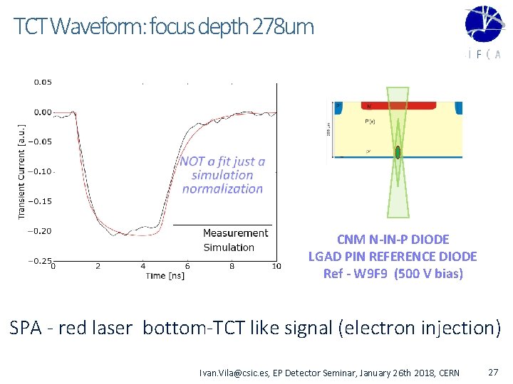
TCT Waveform: focus depth 278 um CNM N-IN-P DIODE LGAD PIN REFERENCE DIODE Ref - W 9 F 9 (500 V bias) SPA - red laser bottom-TCT like signal (electron injection) Ivan. Vila@csic. es, EP Detector Seminar, January 26 th 2018, CERN 27
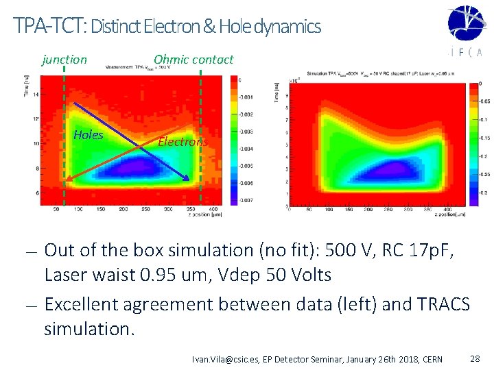
TPA-TCT: Distinct Electron & Hole dynamics junction Holes Ohmic contact Electrons Out of the box simulation (no fit): 500 V, RC 17 p. F, Laser waist 0. 95 um, Vdep 50 Volts — Excellent agreement between data (left) and TRACS simulation. — Ivan. Vila@csic. es, EP Detector Seminar, January 26 th 2018, CERN 28
TPA-TCT Proof-of-concept Challenges 1. 2. 3. Confirm the generation of TPA induced current in a silicon diode with the appropriate laser power. Determine the dimensions of the charge-carrier’s generation volume. Compare the experimental TCT current waveforms against theoretical simulated current waveforms. Ivan. Vila@csic. es, EP Detector Seminar, January 26 th 2018, CERN 29
Part 3 -1 Exploit the recipe: cases of use — Radiation damage on LGAD diodes — High-resolution HV-CMOS Deep n-well junction mapping Ivan. Vila@csic. es, EP Detector Seminar, January 26 th 2018, CERN 30
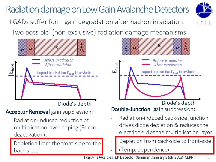
Radiation damage on Low Gain Avalanche Detectors Impact ionization Efield threshold Diode’s depth Acceptor Removal gain suppression: Radiation-induced reduction of multiplication layer doping (Boron deactivation). Depletion from the front-side to the back-side. n+ p++ p n++ p+ p++ p Before irradiation After irradiation |Efield| n++ p+ LGADs suffer form gain degradation after hadron irradiation. Two possible (non-exclusive) radiation damage mechanisms: Before irradiation After irradiation Impact ionization Efield threshold Diode’s depth Double-Junction gain suppression: Radiation-induced back-side junction drives diode depletion & reduces the electric field at the multiplication layer Depletion from back-side to front-side. (Temp. dependence) Ivan. Vila@csic. es, EP Detector Seminar, January 26 th 2018, CERN 31
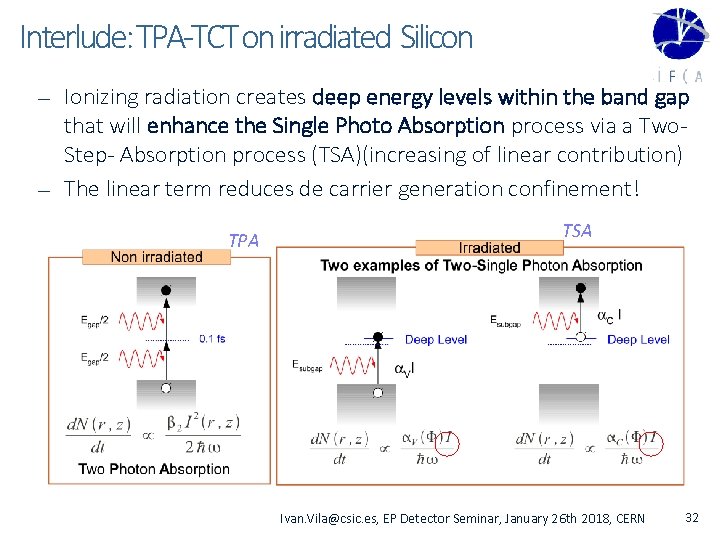
Interlude: TPA-TCT on irradiated Silicon — — Ionizing radiation creates deep energy levels within the band gap that will enhance the Single Photo Absorption process via a Two. Step- Absorption process (TSA)(increasing of linear contribution) The linear term reduces de carrier generation confinement! TPA TSA Ivan. Vila@csic. es, EP Detector Seminar, January 26 th 2018, CERN 32
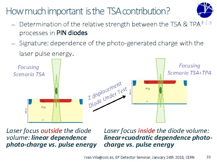
How much important is the TSA contribution? — — Determination of the relative strength between the TSA & TPA processes in PIN diodes Signature: dependence of the photo-generated charge with the laser pulse energy. Focusing Scenario TSA+TPA Focusing Scenario TSA nt e cem Test a l isp nder d Z e. U d Dio Laser focus outside the diode volume: linear dependence photo-charge vs. pulse energy Laser focus inside the diode volume: linear+cuadratic dependence photocharge vs. pulse energy Ivan. Vila@csic. es, EP Detector Seminar, January 26 th 2018, CERN 33
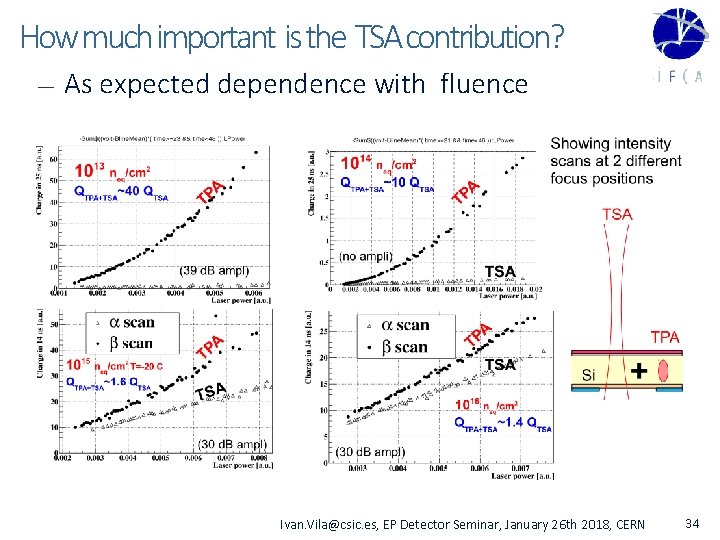
How much important is the TSA contribution? — As expected dependence with fluence Ivan. Vila@csic. es, EP Detector Seminar, January 26 th 2018, CERN 34
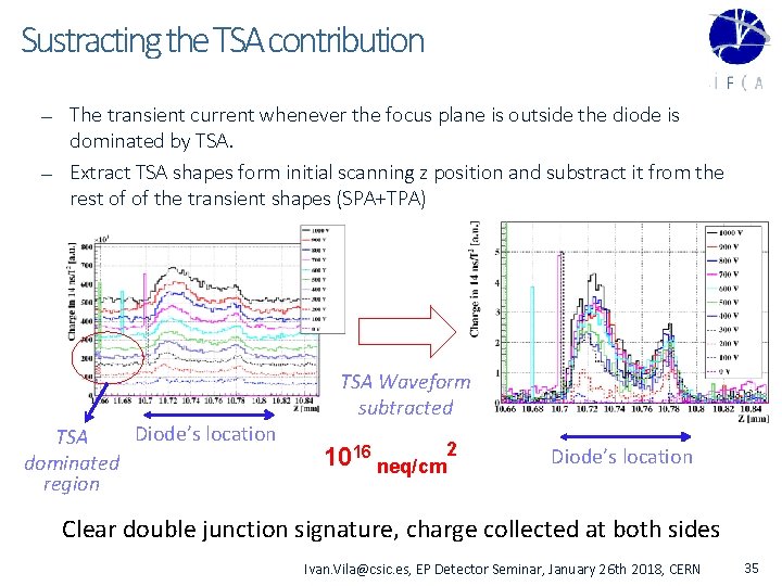
Sustracting the TSA contribution — — The transient current whenever the focus plane is outside the diode is dominated by TSA. Extract TSA shapes form initial scanning z position and substract it from the rest of of the transient shapes (SPA+TPA) TSA Waveform subtracted Diode’s location TSA dominated region 1016 neq/cm 2 Diode’s location Clear double junction signature, charge collected at both sides Ivan. Vila@csic. es, EP Detector Seminar, January 26 th 2018, CERN 35
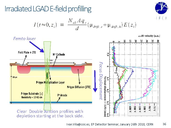
Irradiated LGAD E-field profilling Femto laser Focus Displacement Clear Double Juntion profiles with depletion starting at the back side. Ivan. Vila@csic. es, EP Detector Seminar, January 26 th 2018, CERN 36
Part 3 -2 Exploit the recipe: cases of use — Radiation damage on LGAD diodes — High-resolution HV-CMOS Deep n-well junction mapping Ivan. Vila@csic. es, EP Detector Seminar, January 26 th 2018, CERN 37
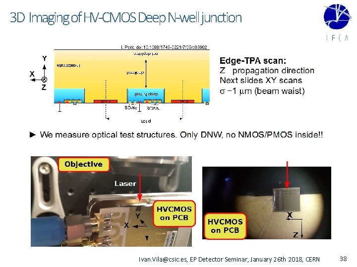
3 D Imaging of HV-CMOS Deep N-well junction Ivan. Vila@csic. es, EP Detector Seminar, January 26 th 2018, CERN 38
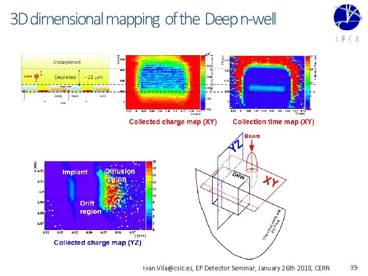
3 D dimensional mapping of the Deep n-well Ivan. Vila@csic. es, EP Detector Seminar, January 26 th 2018, CERN 39
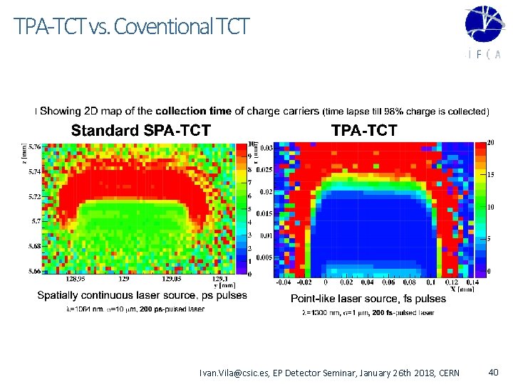
TPA-TCT vs. Coventional TCT Ivan. Vila@csic. es, EP Detector Seminar, January 26 th 2018, CERN 40
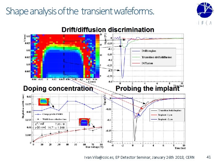
Shape analysis of the transient wafeforms. Ivan. Vila@csic. es, EP Detector Seminar, January 26 th 2018, CERN 41
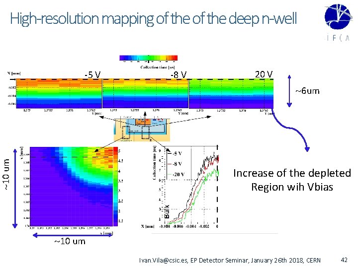
High-resolution mapping of the deep n-well -5 V -8 V 20 V 10 um 6 um Increase of the depleted Region wih Vbias 10 um Ivan. Vila@csic. es, EP Detector Seminar, January 26 th 2018, CERN 42
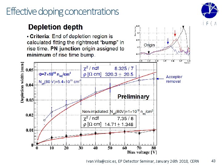
Effective doping concentrations Ivan. Vila@csic. es, EP Detector Seminar, January 26 th 2018, CERN 43
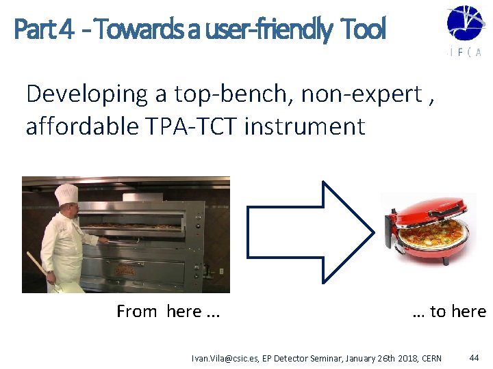
Part 4 - Towards a user-friendly Tool Developing a top-bench, non-expert , affordable TPA-TCT instrument From here. . . … to here Ivan. Vila@csic. es, EP Detector Seminar, January 26 th 2018, CERN 44
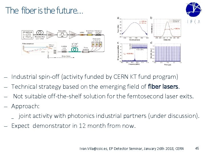
The fiber is the future… — — — Industrial spin-off (activity funded by CERN KT fund program) Technical strategy based on the emerging field of fiber lasers. Not suitable off-the-shelf solution for the femtosecond laser exits. Approach: _ joint activity with photonics industrial partners (under discussion). Expect demonstrator in 12 month from now. Ivan. Vila@csic. es, EP Detector Seminar, January 26 th 2018, CERN 45
Conclusions — A Sub-bandgap NIR Femtosecond-laser based TCT (TPA-TCT) has important advantages with respect to conventional NIR laser : _ _ — Enabling technique (unique insights): _ Mapping of double-(multi)-junction effect induced by radiation on LGADs. _ — Confined carrier generation in the focus region. High-resolution 3 D mapping of the charge collecting junction and simpler unfolding of sensor’s performance characteristics. Carrier generation time very short with respect to the transient, recombination effects or other carrier dynamics. First distinct 3 D mapping of the deep n-well on HV-CMOS devices. A top-bench scale, turn-key solution in development. Ivan. Vila@csic. es, EP Detector Seminar, January 26 th 2018, CERN 46
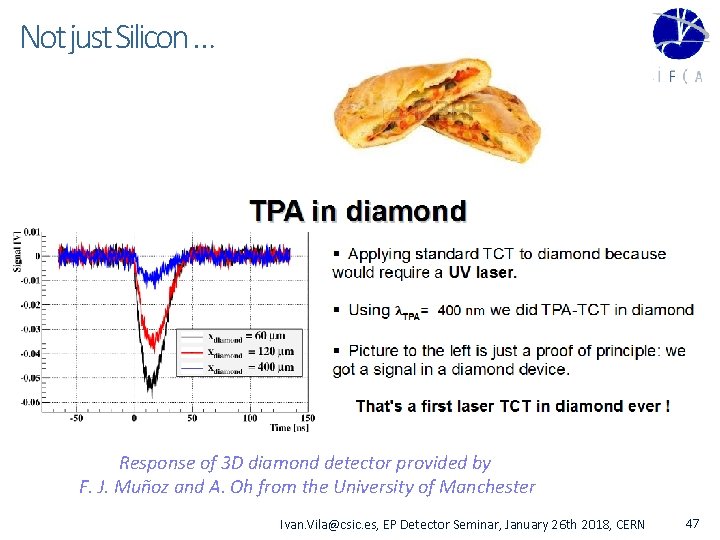
Not just Silicon … Response of 3 D diamond detector provided by F. J. Muñoz and A. Oh from the University of Manchester Ivan. Vila@csic. es, EP Detector Seminar, January 26 th 2018, CERN 47
THANK YOU FOR YOUR ATTENTION ! Two Photon Absorption and carrier generation in semiconductors https: //indico. cern. ch/event/334251/contributions/780784/ A novel Transient Current Technique based on the Two Photon Absorption (TPA) process https: //indico. cern. ch/event/334251/contributions/780782/ Characterization of neutron irradiated pad detectors using a Transient Current Technique based on the Two Photon Absorption process (TPA-TCT) https: //agenda. infn. it/contribution. Display. py? contrib. Id=41&conf. Id=11109 High-resolution three-dimensional imaging of a depleted CMOS sensor using an edge Transient Current Technique based on the Two Photon Absorption process (TPA-e. TCT), NIM A, http: //dx. doi. org/10. 1016/j. nima. 2016. 05. 070 On the determination of the substrate effective doping concentration of irradiated HV-CMOS sensors using an edge-TCT technique based on the Two. Photon-Absorption process. JINST 025 P 1116, Ivan. Vila@csic. es, EP Detector Seminar, January 26 th 2018, CERN 48
- Slides: 48