Towards Edge Computing CoDesign for Machine Learning based

Towards Edge Computing: Co-Design for Machine Learning based ASICs for Scientific Applications Sandeep Miryala, Gabriella Carini, Grzegorz Deptuch, Jack Fried, Jin Huang, Florence Lucey, Yihui Ren, Shinjae Yoo Brookhaven National Laboratory smiryala@bnl. gov
Outline • Introduction • Readout integrated circuits – signal processing chain • Future readout ASIC architecture • Waveform processing using Machine Learning (ML) algorithms • Exploring various neural networks (MLP, CNN etc. ) • Optimization of a neural network • Hardware-software co-design • Hardware design • Introduction of memristor • Behavioral modeling • Memristor crossbar arrays
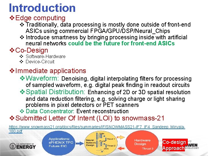
Introduction v. Edge computing v Traditionally, data processing is mostly done outside of front-end ASICs using commercial FPGA/GPU/DSP/Neural_Chips v Introduce smartness by bringing processing inside with artificial neural networks could be the future for front-end ASICs v. Co-Design v Software-Hardware v Device-Circuit v. Immediate applications v. Waveform: Denoising, digital interpolating filters for processing of sampled waveform, e. g. digital peak finding in readout circuits v. Spatial Distribution: Enhancing of 2 D or 3 D spatial resolution and data reduction filtering, e. g. solving charge or light sharing problems in pixel detectors or PET scanners v Data Concentrator: Event reconstruction v. Submitted Letter Of Intent (LOI) to snowmass-21 https: //www. snowmass 21. org/docs/files/summaries/IF/SNOWMASS 21 -IF 7_IF 4_Sandeep_Miryala 180. pdf Co-design Approach
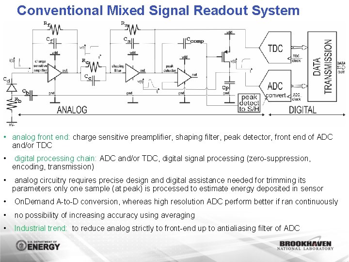
Conventional Mixed Signal Readout System • analog front end: charge sensitive preamplifier, shaping filter, peak detector, front end of ADC and/or TDC • digital processing chain: ADC and/or TDC, digital signal processing (zero-suppression, encoding, transmission) • analog circuitry requires precise design and digital assistance needed for trimming its parameters only one sample (at peak) is processed to estimate energy deposited in sensor • On. Demand A-to-D conversion, whereas high resolution ADC perform better if ran continuously • no possibility of increasing accuracy using averaging • Industrial trend: to reduce analog strictly to front-end up to antialiasing filter of ADC
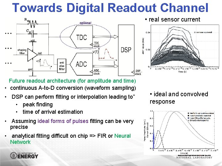
Towards Digital Readout Channel • real sensor current Future readout architecture (for amplitude and time) • continuous A-to-D conversion (waveform sampling) • DSP can perform fitting or interpolation leading to” • peak finding • time of arrival estimation • Assuming ideal forms of pulses fitting can be very precise • analytical fitting difficult on chip => FIR or Neural Network • ideal and convolved response
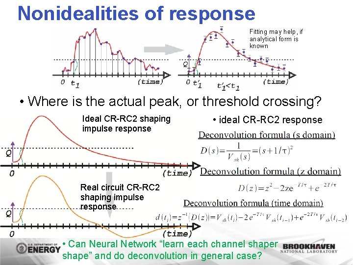
Nonidealities of response Fitting may help, if analytical form is known • Where is the actual peak, or threshold crossing? Ideal CR-RC 2 shaping impulse response • ideal CR-RC 2 response Real circuit CR-RC 2 shaping impulse response • Can Neural Network “learn each channel shaper shape” and do deconvolution in general case?
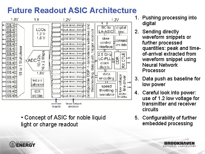
Future Readout ASIC Architecture 1. Pushing processing into digital 2. Sending directly waveform snippets or further processed quantities: peak and timeof-arrival extracted from waveform snippet using Neural Network Processor 3. Data push as baseline for low power 4. Careful look into power: use of 1. 2 low voltage for transmitter and receiver circuits • Concept of ASIC for noble liquid light or charge readout 5. Configurability of further embedded processing
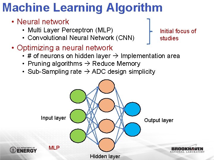
Machine Learning Algorithm • Neural network • Multi Layer Perceptron (MLP) • Convolutional Neural Network (CNN) Initial focus of studies • Optimizing a neural network • # of neurons on hidden layer Implementation area • Pruning algorithms Reduce Memory • Sub-Sampling rate ADC design simplicity Input layer Output layer MLP Hidden layer
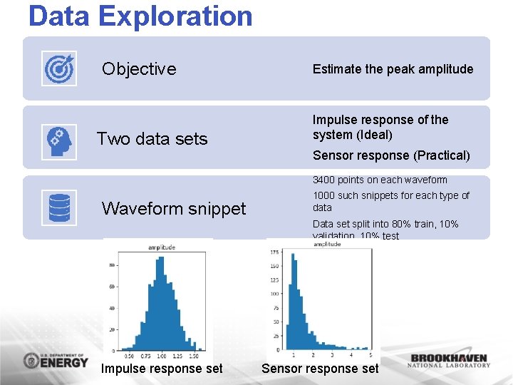
Data Exploration Objective Two data sets Estimate the peak amplitude Impulse response of the system (Ideal) Sensor response (Practical) 3400 points on each waveform Waveform snippet Impulse response set 1000 such snippets for each type of data Data set split into 80% train, 10% validation, 10% test Sensor response set
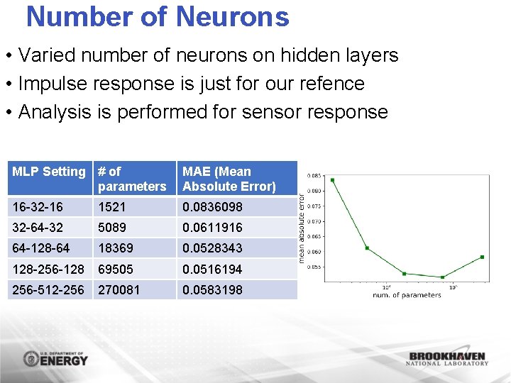
Number of Neurons • Varied number of neurons on hidden layers • Impulse response is just for our refence • Analysis is performed for sensor response MLP Setting # of parameters MAE (Mean Absolute Error) 16 -32 -16 1521 0. 0836098 32 -64 -32 5089 0. 0611916 64 -128 -64 18369 0. 0528343 128 -256 -128 69505 0. 0516194 256 -512 -256 270081 0. 0583198
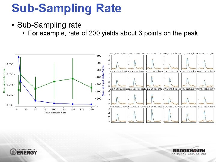
Sub-Sampling Rate • Sub-Sampling rate • For example, rate of 200 yields about 3 points on the peak
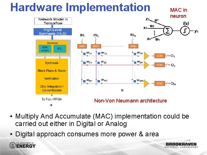
Hardware Implementation MAC in neuron Non-Von Neumann architecture • Multiply And Accumulate (MAC) implementation could be carried out either in Digital or Analog • Digital approach consumes more power & area
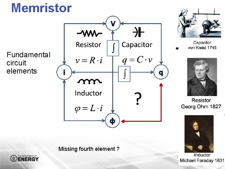
Memristor Fundamental circuit elements Missing fourth element ?
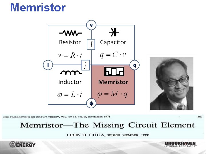
Memristor
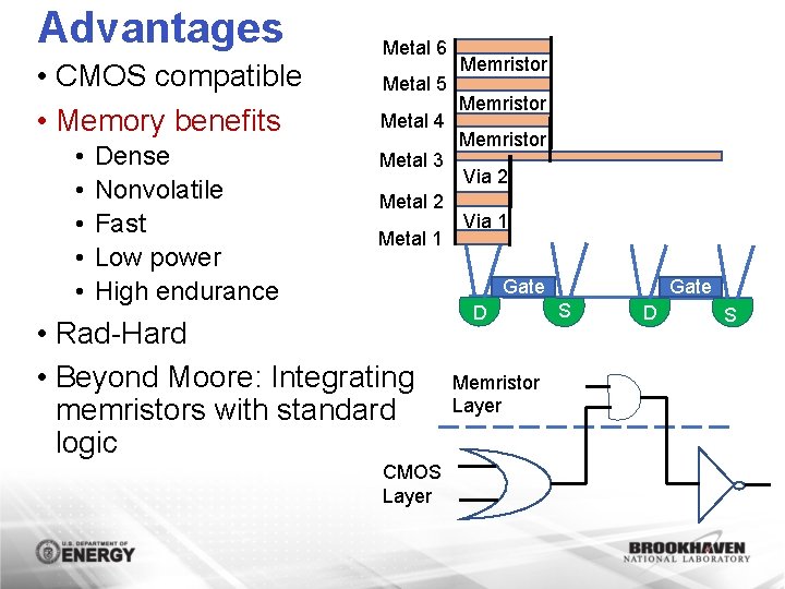
Advantages • CMOS compatible • Memory benefits • • • Dense Nonvolatile Fast Low power High endurance Metal 6 Metal 5 Metal 4 Metal 3 Metal 2 Metal 1 Memristor Via 2 Via 1 Gate • Rad-Hard • Beyond Moore: Integrating memristors with standard logic CMOS Layer D Memristor Layer S D S
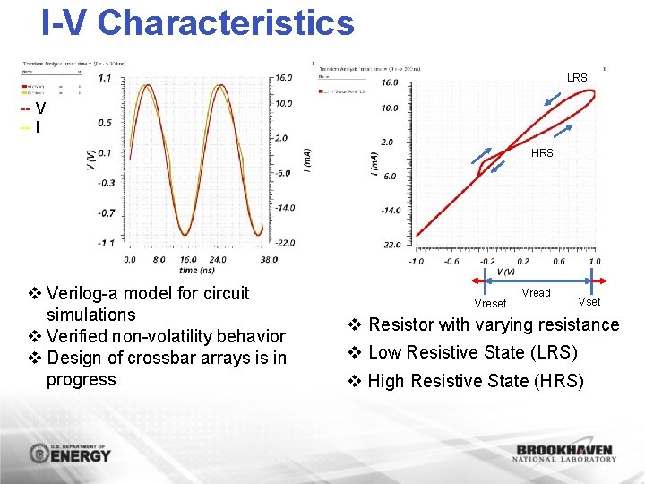
I-V Characteristics LRS -- V -- I HRS v Verilog-a model for circuit simulations v Verified non-volatility behavior v Design of crossbar arrays is in progress Vreset Vread Vset v Resistor with varying resistance v Low Resistive State (LRS) v High Resistive State (HRS)
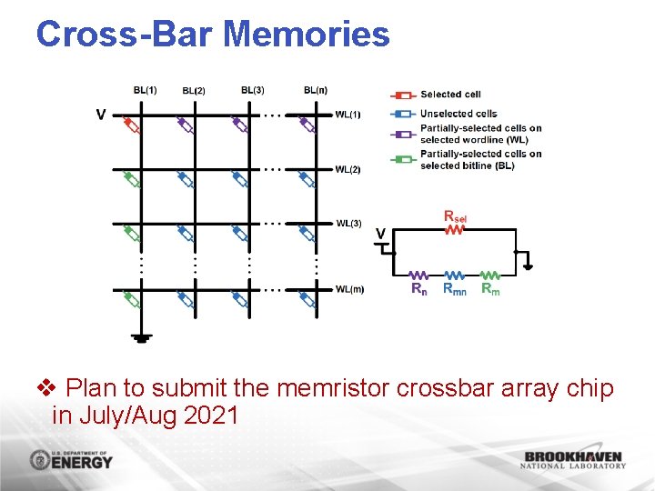
Cross-Bar Memories v Plan to submit the memristor crossbar array chip in July/Aug 2021
Acknowledgements • Towards Edge Computing LDRD • Collaboration between Instrumentation Division (IO) and Computational Science Initiative (CSI) • https: //www. bnl. gov/ldrd/ • External collaborators • Argonne National Laboratory (ANL) • University of South Florida (USF) • Others …
- Slides: 18