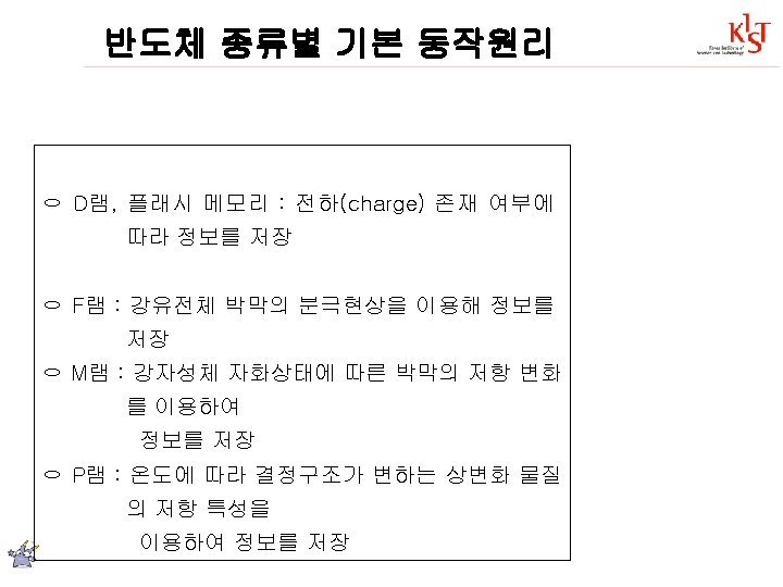
Total MOS Memory Volatile NonVolatile Read Only Memory
 Volatile Non-Volatile Read Only Memory (ROM) Random Access Memory")
 Read")


 (router/hub) Solid-State Disk")


 •")
 •")


 MRAM DRAM EEPROM SRAM FRAM Cell")
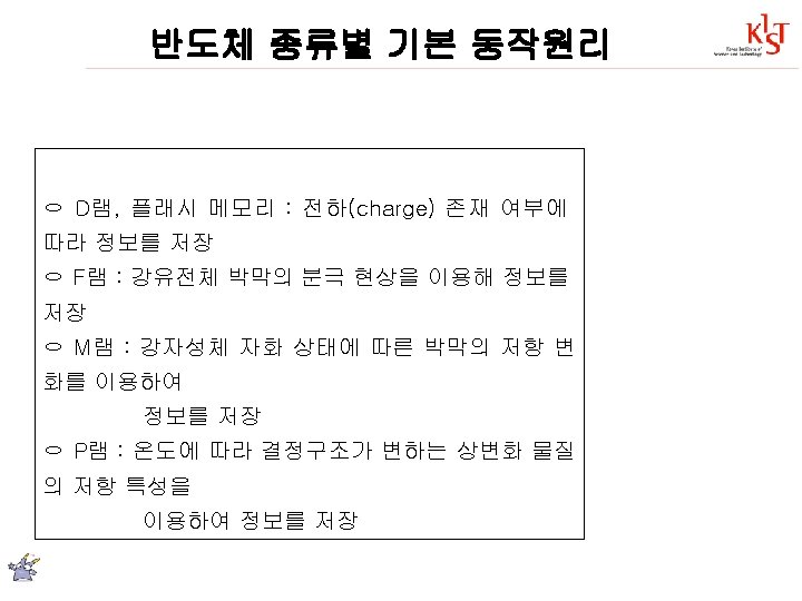


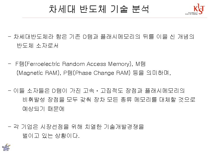
와 다른 점 DRAM TMR")
 Word line Current Free")
 Magneti c reversal X")
 Only the element at the intersection is")


 • Thermally")


")
")
")


 spin injection: very low efficiency (~1%) (ii) spin")
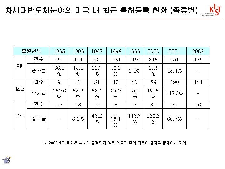
 순위 기업체 등록건수 1 Micron Technology")
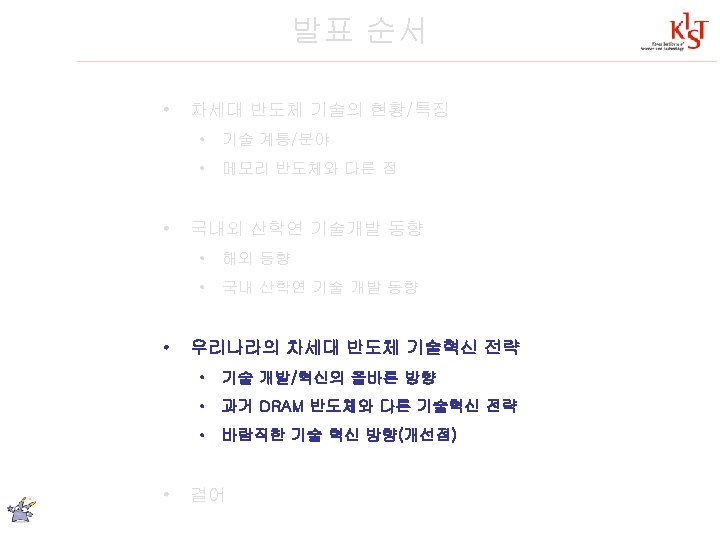


- Slides: 63
Total MOS Memory……(현재 상품 단계) Volatile Non-Volatile Read Only Memory (ROM) Random Access Memory (RAM) Dynamic RAM Static RAM Programmable ROM EPROM EEPROM FALSH Mask ROM NVRAM Kwangwoon University Magneto electronics Lab
NVM Classifications • • ROM EPROM EEPROM FLASH : : (현재 => 미래) Read Only Memory (UV) Erasable Programmable ROM Electrically Erasable Programmable ROM Flash Erase EEPROM (Single, Multilevel) • FERRO-ELECTRIC MEMORY , MRAM, • PRAM, NFGM, RRAM, Po. RAM, • ( Spin FET, SET, CNT etc. ) Y. T. Lee, Samsung Electronics. 발표자료 참조
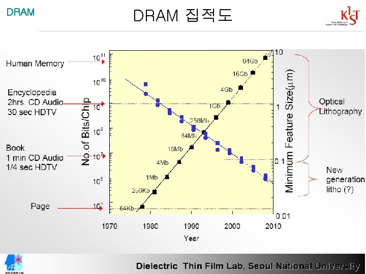
DRAM
DRAM
DRAM
Flash Memory Application Mass Storage Embedded Memory Cards Networking (mobile computers) (router/hub) Solid-State Disk Telecommunications (rugged & reliable storage) (switcher) Digital Camera Cellular Phone (still & moving pictures) (code & data) Voice/Audio Recorder POS / PDA / PCA (near CD quality) (code & data) • Low Cost and power • Good P/E Cycling Endurance • flash memory, High Density • Fast Random Access • High Data Integrity • FRAM, embedding Y. T. Lee, Samsung Electronics. 발표자료 참조
Flash Memory Hot Electrion Injection vs. Fowler-Nordheim Tunneling q Hot Electron Injection q Fowler-Nordheim Tunneling Y. T. Lee, Samsung Electronics. 발표자료 참조
Flash Memory H. V. Requirements in Flash Memory · For Program or Erase Operation (NOR Flash) Program(CHE) No. of Bits OFF ON Vth(V) 1 3 6 8 Erase(FN Tunneling) No. of Bits ON OFF Vth(V) 1 3 6 8 Y. T. Lee, Samsung Electronics. 발표자료 참조
Flash Memory Read Operation Basic Cell Bias Condition Threshold Voltage Distribution ON-Cell Vwordline OFF-Cell Vowrdline (3, 4. 5, 7) Vbitline (~1. 0 V) 1 V 3 V 4. 5 V W/L (Erase Verify) 7 V 8. 5 V W/L (Program Verify) Y. T. Lee, Samsung Electronics. 발표자료 참조
Flash Memory NVM Cell Structure q EPROM Cell Structure (UV Erasable Programmable ROM) • • • Single TR NMOS Floating Gate Device FAMOS (Floating Gate Avalanche Injection MOS) Program : Hot-Electron Injection Erase : UV Light Program in factory => product. (NFGM) Nano Floating Gate Memory -Nano dots -Nano FG Control Gate Floating Gate Poly/Poly Dielectric Gate Oxide N+ N+ P-Substrate Y. T. Lee, Samsung Electronics. 발표자료 참조
Flash Memory NVM Cell Structure q EEPROM Cell Structure (Electrically Erasable Programmable ROM) • Two Transistor Cell with FLOTOX (Floating Gate Tunnel Oxide) • Program, Erase : Fowler-Nordheim(FN) Tunneling • F-N Tunneling : Slower Than Hot-Electron Injection Less Current Than Hot-Electron Injection Control Gate Floating Gate Tunnel Oxide Select Tr. N+ N+ P-Substrate Y. T. Lee, Samsung Electronics. 발표자료 참조
Flash Memory NVM Cell Structure q NOR-Type Flash Cell Structure • • One Transistor NMOS Floating Gate Device ETOX (EPROM Tunnel Oxide) Program : Hot-Electron Erase : F-N Tunneling Control Gate Floating Gate Poly/Poly Dielectric Tunnel Oxide N+ N+ P-Substrate Y. T. Lee, Samsung Electronics. 발표자료 참조
Flash Memory NVM Cell Structure q NAND-Type Flash Cell Structure • One Transistor NMOS Floating Gate Device • Program : F-N Tunneling • Erase : F-N Tunneling Control Gate Floating Gate N+ P-Substrate Y. T. Lee, Samsung Electronics. 발표자료 참조
Flash Memory Features of NAND- and NOR-type EEPROM’s Merits of NAND Merits of NOR ①High speed programming ①High speed random access ②High speed erasing ②Byte programming ③Small block size Demerits of NAND Demerits of NOR ①Slow random access ①Slow programming ②Byte programming can not be performed ②Slow speed erasing - Applications - Suitable for Data memory (Handy terminal, Voice recorder, DSC, Fax modem, etc) 삼성, 하이닉스 생산 - Applications - Suitable for replacement of EPROM Suitable for control memory (BIOS, Cellular, HDD, etc) Y. T. Lee, Samsung Electronics. 발표자료 참조
Flash Memory NVM Cell Type별 Comparison NOR NAND Flash EPROM EEPROM Vcc 5 V/12 V 5 V 5 V, 3. 3 V Cell 1 Tr. 2 Tr. 1 Tr. P/E Cycling ~ 103 ~ 105 ~ 106 Program Hot-Elec. F-N Erase UV-Light F-N F-N PGM Speed 10 us/Byte 5 ms/Byte 10 us/Byte 300 us/512 Byte Erase Speed 32 min/Chip 10 ms/Chip 1 s/64 k. Byte 5 ms/16 k. Byte Y. T. Lee, Samsung Electronics. 발표자료 참조
Flash Memory Future Flash Memory Hand-held Application Power Supply Voltage Trend Single + Low Power Supply 6 5 To Meet This Requirement, 4 Vcc[V] 3 Key Limiting Factor is H. V. Generation at Lower Power Supply Voltage 2 (ISSCC, VLSI) 1 90 92 94 96 98 Year Y. T. Lee, Samsung Electronics. 발표자료 참조
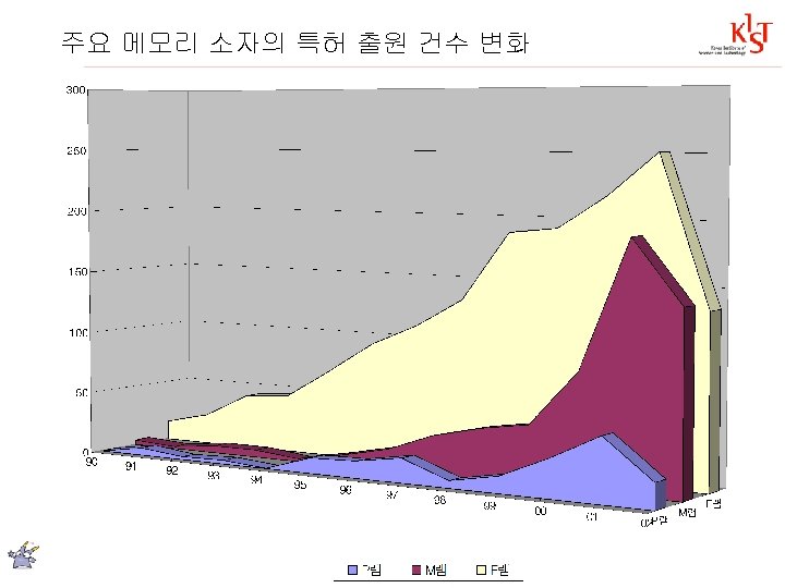
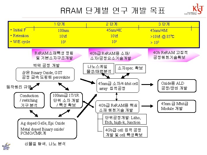
차세대 반도체기술 동향 (NVM, 산업화 단계 진입. ) MRAM DRAM EEPROM SRAM FRAM Cell Structure 1 TR+1 TMR 1 TR+1 Cap 1 TR 6(4)TR 1 TR+1 Cap Density High Low Low Non-Volatility ○ X ○ Speed(R/W) 10~50 ns 20~110 ns 100~130 ns No. Rewrite 1015 105 1012 Power 10~400 m. W 100 m. W 1100 m. W 2 m. W Power dissipation Small Large Very small Application Main memory Flash memory Cache memory IC card Terabit 급 Embedded Kwangwoon University Magneto electronics Lab
Ferroelectric RAM • Oxide • FRAM : Pb. Zr. Ti. O 3 , Sr. Bi. Ta. O 9 • Polymer RAM
Ferroelectric Memory
Ferroelectric Memory
Magnetic RAM Storage element smaller than MOSFET - 메모리 반도체(DRAM)와 다른 점 DRAM TMR MRAM Kwangwoon University Magneto electronics Lab
Magnetic RAM Basic structure of MRAM…… MTJ (Magnetic Tunnel Junction) Word line Current Free layer Insulating Barrier Pinned layer(FM) Read line Parallel moments Low resistance Pinning layer(AFM) Anti parallel moments High resistance Kwangwoon University Magneto electronics Lab
Magnetic RAM Operating system of MRAM…… State : 0 (a) Magneti c reversal X Magnetic field State : 1 Current Writing with Magnetic field Y & (b) Current Voltage V 0 Voltage V 1(>V 0) Kwangwoon University Reading with Voltage Magneto electronics Lab
Magnetic RAM Bit cell…. . ! (a) Only the element at the intersection is rewritten Word Line Current Bit Line Y X Current (b) View from above Current Y X Sum of magnetic field Current Reversal of magnetization Field generated by Current in Y direction Orientation unchanged Kwangwoon University Magneto electronics Lab
Magnetic RAM MTJ
Magnetic RAM 1 T 1 MTJ MRAM
Magnetic RAM Physical Cross Section
Magnetic RAM Memory 특성 비교
Resistive RAM 차세대 비휘발성 메모리 Intel web site
Resistive RAM • Phase Change Memory • Chalcogenide (Ge. Se. . ) • Thermally induced phase change => Resistive change (Logic states) • Thermal Isolation : High density cells • Resistive Switching Memory • Ni. O, Cr doped Sr. Zr. O 3, Pr. Ca. Mn. O. • Filaments, Forming (? ) => Resistive change (Logic states)
Resistive RAM
Resistive RAM 기존 국내외 연구 개발 현황 – Perovskite oxides Pr 0. 7 Ca 0. 3 Mn. O 3 • B-site substitution by Al 3+, Fe 3+, Mn 3+, Cr 3+ decrease in the leakage current Cr-STO , Cr-SZO, . .
Resistive RAM 저항 변화 메모리 (RRAM)
Resistive RAM 저항 변화 메모리 (RRAM)
Resistive RAM 저항 변화 메모리 (RRAM)
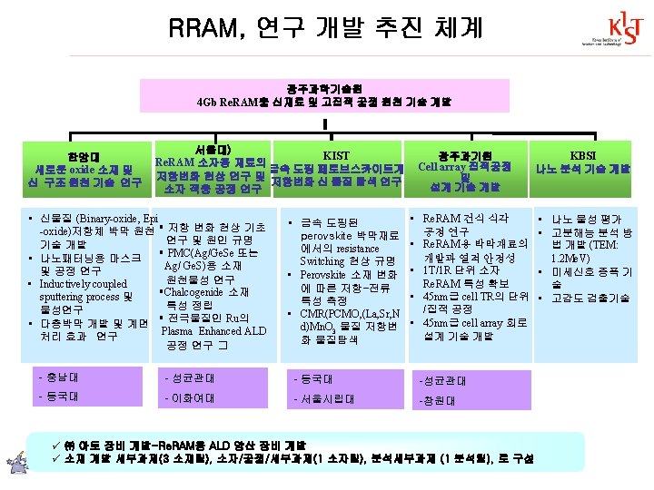
비휘발성 메모리 소자 종합 비교 Function DRAM SRAM Flash MRAM PRAM NFGM Po. RAM Re. RAM Non-volatility No No Yes Yes Yes Program power Low High Low Low Program voltage Low High Medium Low Low Write-Erase time 50 ns 8 ns-8 ns 1 us 1~100 ms 30 ns <50 ns 10 ns -30 ns <10 ns 30 ns Read time 50 ns 8 ns 50 ns 30 ns 20 ns Program energy Medium High Medium Low Low Multi-bit storage No No Yes Yes Yes Scalability limits Capacitor 6 T T-Ox/HV Current Litho. Endurance ∞ ∞ 1012 ? 1015 Cell size(F 2) 6~12 50~80 7~11 ? 6 6 ? 4~6 ü 기존 플래시 메모리 소자는 10 ~ 15 V 고전압을 사용한 Write/Erase 동작으로 인해 집적도 16 Gb, 읽는 속도 8㎲, 저장속도 1㎳ 가 한계임 (신뢰성 문제 유발) ü 초고속화 (수십nsec이하), 고집적도(1 Terr bit이상), 고신뢰성 (W/E cycle 106 이상) 및 저 전압동작에 적합한 2010년 이후 상용화될 차세대 Re. RAM 소자 개발이 절실히 필요함
비휘발성 메모리 소자 특성비교 Baseline 2004 Technologies PRAM NFGM Po. RAM Re. RAM Storage Mechanism Device Types DRAM NOR Flash OUM Engineered tunnel barrier or nanocrystal Bistable Switch MIM Availability 2004 ~2006 >2010 ~2010 Cell Elements 1 T 1 C 1 T 1 T 1 R F Value 90 nm 100 nm 80 nm 45 nm 65 nm Cell Size 8 F 2 0. 065 µm 2 12. 5 F 2 0. 101 µm 2 ~6 F 2 0. 06 µm 2 4 to 10 F 2 0. 04 µm 2 4 F 2 ~0. 008 µm 2[I] 6 F 2 0. 025 µm 2[C] Write/Erase Time 50 ns 1 us/1 ms <100 ns 10 ns <10 ns 50 ns/ <100 ns Retention Time 64 ms 10 -20 years >10 years > 1 year >1 year E/W Cycles Infinite >1 E 5 >1 E 13 >1 E 6 >1 E 15 >1 E 3 Re. RAM의 소자구조는 1 T+1 R형이 제시되고 있음 Po. RAM의 시장 출시는 2010년 이후로 ITRS(2003)는 예견하고 있음 F: min. feature size, Half metal pitch
Spintronics Spin FET structure (i) spin injection: very low efficiency (~1%) (ii) spin transport (iii) control / manipulation for desired functionality (iv) detection of spin-polarized carriers Spin FET: Theoretical ideas proposed by Datta and Das [APL 56, 665 (1990)] The effective electric field can alter the spin precession by applying Vg to control.
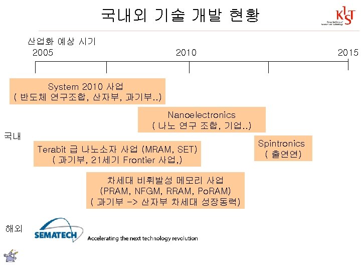
차세대반도체 미국 내 특허등록 기업체 별 현황 (1995~2003) 순위 기업체 등록건수 1 Micron Technology 239 6 Samsung 94 2 Infineon Technologies 126 6 Sharp 94 3 Hynix 125 8 Toshiba 90 4 Motorola 119 9 Symetrix 72 5 Hewlett Packard 101 10 Ramtron 67
SEMATECH is the world's catalyst for accelerating the commercialization of technology innovations into manufacturing solutions. By setting global direction, creating opportunities for flexible collaboration, and conducting strategic R&D, SEMATECH delivers significant return on investment to our semiconductor and emerging technology partners.
What we do…. SEMATECH At SEMATECH, we work with our members and partners to reduce the time from innovation to manufacturing. Our role is to address critical challenges in advanced technology and manufacturing effectiveness, and to find ways to speed development, reduce costs, share risks, and increase productivity.
SEMATECH Full SEMATECH membership – SEMATECH's Advanced Technology divisions conduct state-of-the-art research on the technical challenges and costs associated with developing new materials, processes, and equipment for semiconductor manufacturing including immersion and EUV patterning and resists, low k-effective materials , and high-k materials and next-generation transistors. Full SEMATECH members are also ISMI members, and have access to AMRC programs and results.
SEMATECH Member AMRC - The AMRC is a cooperative research effort involving the state of Texas, SEMATECH, and Texas universities to accelerate the commercialization of advanced research into semiconductor and emerging technologies like nanotech, biotech, and advanced energy applications.
THE END