Total Ionizing Dose Effects in 130 nm Commercial
- Slides: 30

Total Ionizing Dose Effects in 130 -nm Commercial CMOS Technologies for HEP experiments L. Gonella, M. Silvestri, S. Gerardin on behalf of the DACEL – CERN collaboration

Outline • Introduction & DACEL • Experimental and Devices • TID irradiation (X-rays): – Core transistors: • Worst-case bias conditions – NMOSFETs – PMOSFETs • Impact of bias • Different foundries – I/O transistors: • Worst-case bias conditions – NMOSFETs – PMOSFETs • Impact of bias and foundry • Conclusions Perugia, 26/9/2006 S. Gerardin

DACEL • Design And Characterization of deep submicron ELectronic devices for future particle detectors • Born in 2004 • Participating Institutions – INFN sections: • Bari • Bologna • Firenze • Padova • Torino • In collaboration with CERN-MIC group Perugia, 26/9/2006 S. Gerardin

Introduction • Super LHC radiation environment – Expected up to 100 Mrad in 10 years’ time • Purpose of this work: – Assess the suitability of commercial deep-submicron/ decananometer CMOS technologies for use in future HEP experiments Perugia, 26/9/2006 S. Gerardin

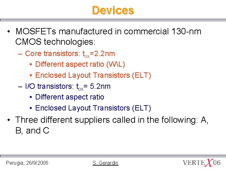
Devices • MOSFETs manufactured in commercial 130 -nm CMOS technologies: – Core transistors: tox=2. 2 nm • Different aspect ratio (WL) • Enclosed Layout Transistors (ELT) – I/O transistors: tox= 5. 2 nm • Different aspect ratio • Enclosed Layout Transistors (ELT) • Three different suppliers called in the following: A, B, and C Perugia, 26/9/2006 S. Gerardin

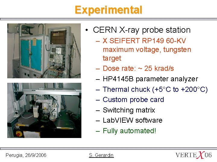
Experimental • CERN X-ray probe station – X SEIFERT RP 149 60 -KV maximum voltage, tungsten target – Dose rate: ~ 25 krad/s – HP 4145 B parameter analyzer – Thermal chuck (+5°C to +200°C) – Custom probe card – Switching matrix – Lab. VIEW software – Fully automated! Perugia, 26/9/2006 S. Gerardin

Core Transistors: Worst Case Bias Conditions Perugia, 26/9/2006 S. Gerardin

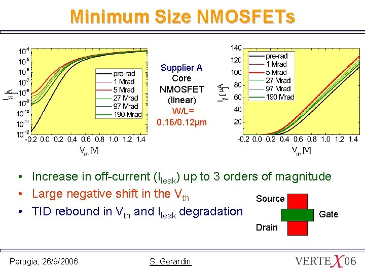
Minimum Size NMOSFETs Supplier A Core NMOSFET (linear) W/L= 0. 16/0. 12µm • Increase in off-current (Ileak) up to 3 orders of magnitude • Large negative shift in the Vth Source • TID rebound in Vth and Ileak degradation Gate Drain Perugia, 26/9/2006 S. Gerardin

Large-width NMOSFETs • Increase in off-current (Ileak) • No shift in the threshold voltage • TID rebound in the Ileak degradation between 5 and 27 Mrad Supplier A Core NMOSFET (linear) W/L= 2/0. 12µm Perugia, 26/9/2006 S. Gerardin

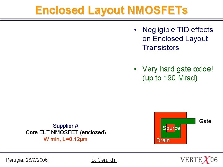
Enclosed Layout NMOSFETs • Negligible TID effects on Enclosed Layout Transistors • Very hard gate oxide! (up to 190 Mrad) Supplier A Core ELT NMOSFET (enclosed) W min, L=0. 12µm Perugia, 26/9/2006 S. Gerardin Gate Source Drain

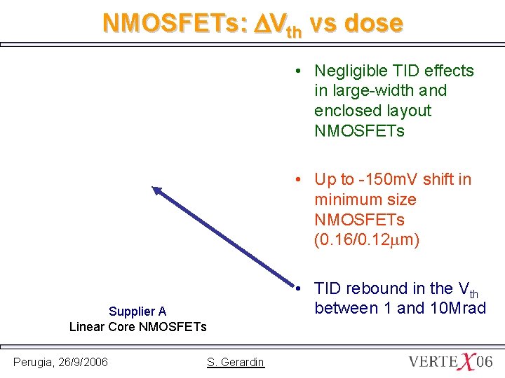
NMOSFETs: DVth vs dose • Negligible TID effects in large-width and enclosed layout NMOSFETs • Up to -150 m. V shift in minimum size NMOSFETs (0. 16/0. 12 mm) • TID rebound in the Vth between 1 and 10 Mrad Supplier A Linear Core NMOSFETs Perugia, 26/9/2006 S. Gerardin

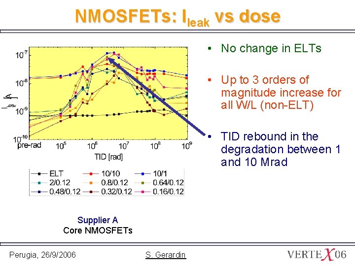
NMOSFETs: Ileak vs dose • No change in ELTs • Up to 3 orders of magnitude increase for all W/L (non-ELT) • TID rebound in the degradation between 1 and 10 Mrad Supplier A Core NMOSFETs Perugia, 26/9/2006 S. Gerardin

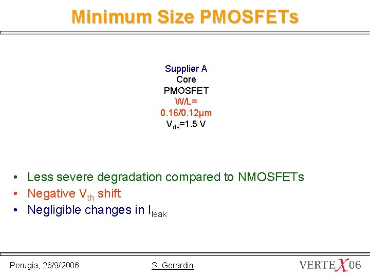
Minimum Size PMOSFETs Supplier A Core PMOSFET W/L= 0. 16/0. 12µm Vds=1. 5 V • Less severe degradation compared to NMOSFETs • Negative Vth shift • Negligible changes in Ileak Perugia, 26/9/2006 S. Gerardin

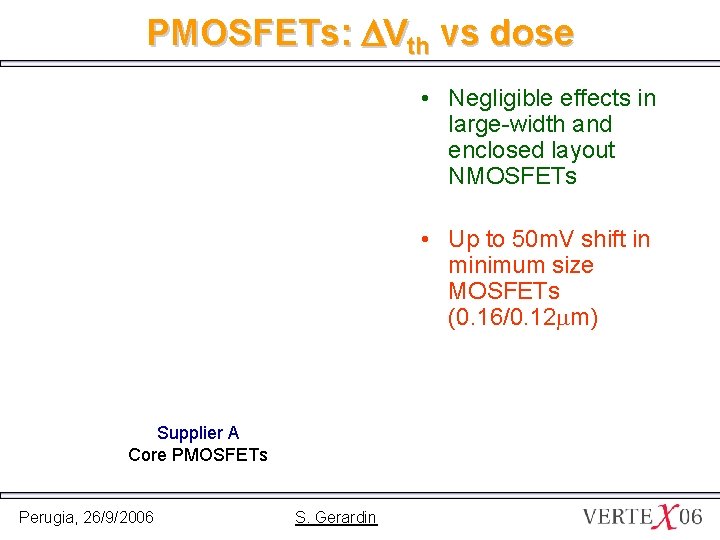
PMOSFETs: DVth vs dose • Negligible effects in large-width and enclosed layout NMOSFETs • Up to 50 m. V shift in minimum size MOSFETs (0. 16/0. 12 mm) Supplier A Core PMOSFETs Perugia, 26/9/2006 S. Gerardin

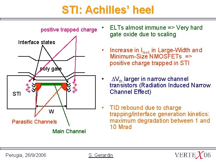
STI: Achilles’ heel positive trapped charge • ELTs almost immune => Very hard gate oxide due to scaling Interface states • Increase in Ileak in Large-Width and Minimum-Size NMOSFETs => positive charge trapped in STI poly gate ++ + ++ STI + W Parasitic Channels Main Channel Perugia, 26/9/2006 • DVth larger in narrow channel transistors (Radiation Induced Narrow Channel Effect) • TID rebound due to charge trapping/interface generation kinetics: maximum degradation between 1 and 10 Mrad S. Gerardin

Core Transistors: Impact of Bias Conditions Perugia, 26/9/2006 S. Gerardin

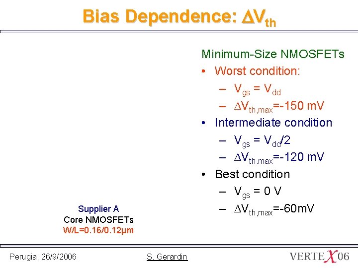
Bias Dependence: DVth Minimum-Size NMOSFETs • Worst condition: – Vgs = Vdd – DVth, max=-150 m. V • Intermediate condition – Vgs = Vdd/2 – DVth. max=-120 m. V • Best condition – Vgs = 0 V – DVth, max=-60 m. V Supplier A Core NMOSFETs W/L=0. 16/0. 12µm Perugia, 26/9/2006 S. Gerardin

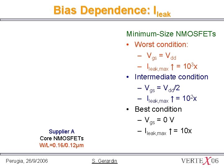
Bias Dependence: Ileak Minimum-Size NMOSFETs • Worst condition: – Vgs = Vdd – Ileak, max ↑ = 103 x • Intermediate condition – Vgs = Vdd/2 – Ileak, max ↑ = 102 x • Best condition – Vgs = 0 V – Ileak, max ↑ = 10 x Supplier A Core NMOSFETs W/L=0. 16/0. 12µm Perugia, 26/9/2006 S. Gerardin

Core Transistors: Different Foundries Perugia, 26/9/2006 S. Gerardin

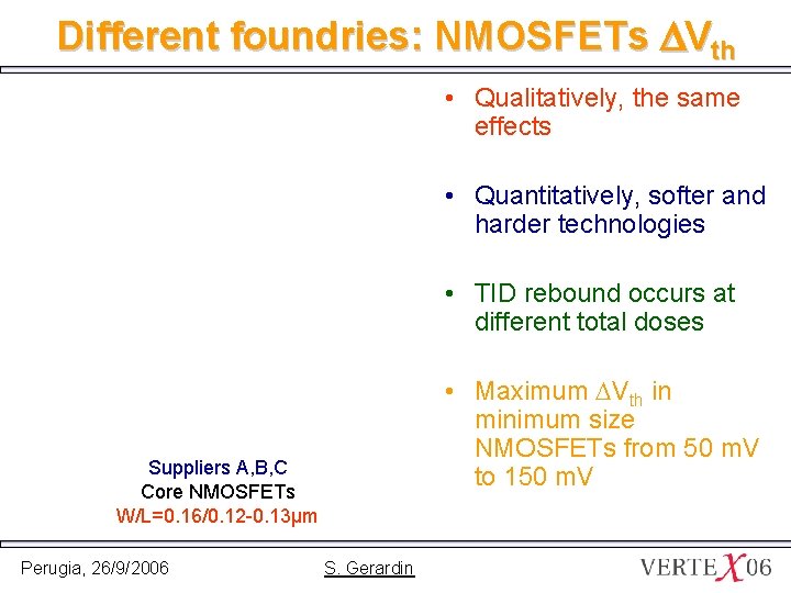
Different foundries: NMOSFETs DVth • Qualitatively, the same effects • Quantitatively, softer and harder technologies • TID rebound occurs at different total doses • Maximum DVth in minimum size NMOSFETs from 50 m. V to 150 m. V Suppliers A, B, C Core NMOSFETs W/L=0. 16/0. 12 -0. 13µm Perugia, 26/9/2006 S. Gerardin

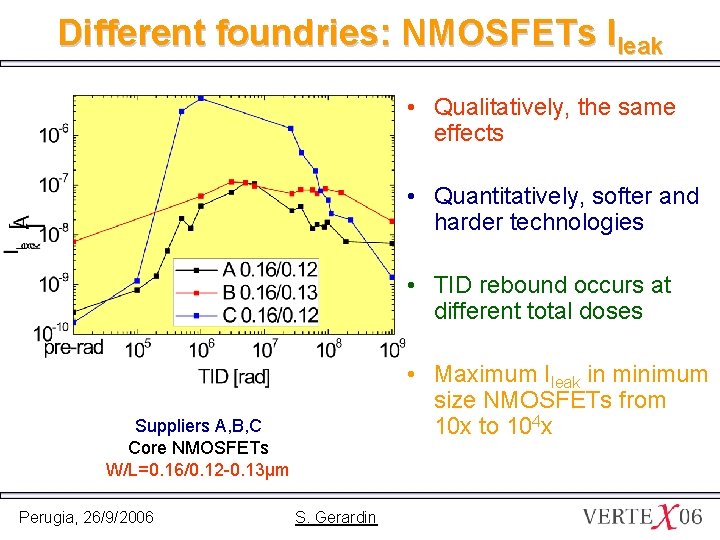
Different foundries: NMOSFETs Ileak • Qualitatively, the same effects • Quantitatively, softer and harder technologies • TID rebound occurs at different total doses • Maximum Ileak in minimum size NMOSFETs from 10 x to 104 x Suppliers A, B, C Core NMOSFETs W/L=0. 16/0. 12 -0. 13µm Perugia, 26/9/2006 S. Gerardin

I/O Transistors: Worst Case Bias Conditions Perugia, 26/9/2006 S. Gerardin

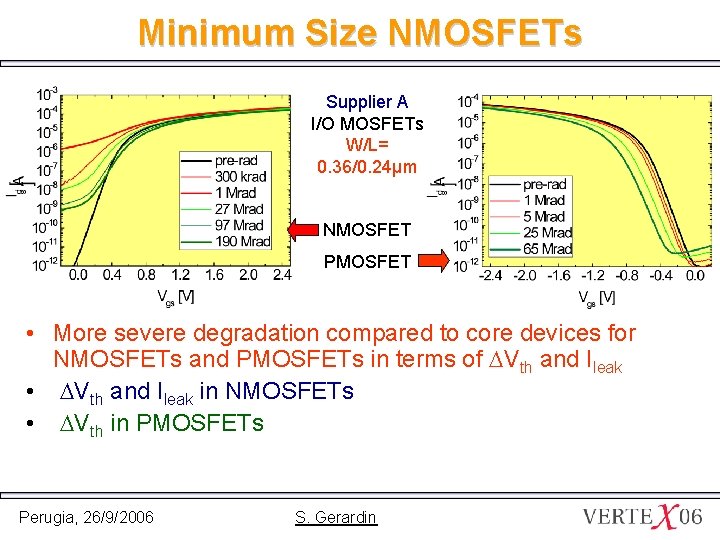
Minimum Size NMOSFETs Supplier A I/O MOSFETs W/L= 0. 36/0. 24µm NMOSFET PMOSFET • More severe degradation compared to core devices for NMOSFETs and PMOSFETs in terms of DVth and Ileak • DVth and Ileak in NMOSFETs • DVth in PMOSFETs Perugia, 26/9/2006 S. Gerardin

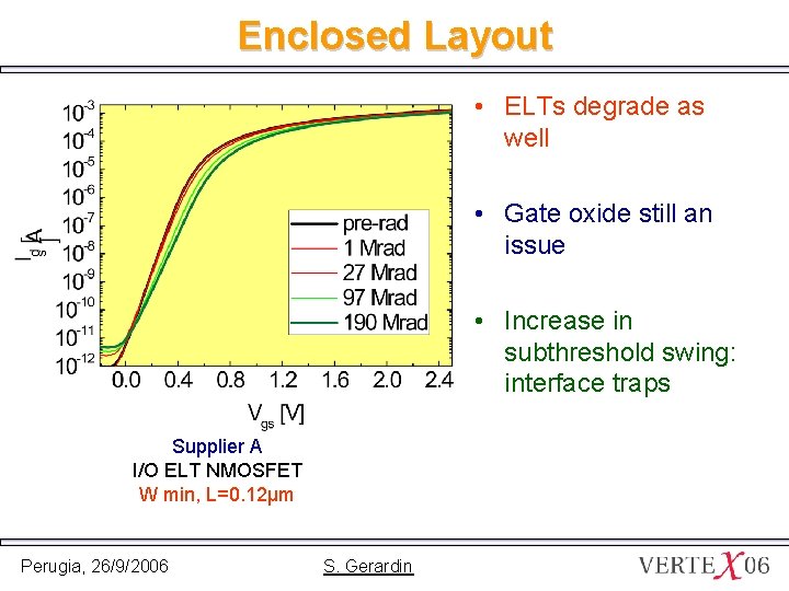
Enclosed Layout • ELTs degrade as well • Gate oxide still an issue • Increase in subthreshold swing: interface traps Supplier A I/O ELT NMOSFET W min, L=0. 12µm Perugia, 26/9/2006 S. Gerardin

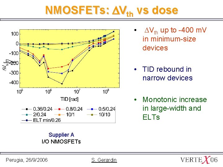
NMOSFETs: DVth vs dose • DVth up to -400 m. V in minimum-size devices • TID rebound in narrow devices • Monotonic increase in large-width and ELTs Supplier A I/O NMOSFETs Perugia, 26/9/2006 S. Gerardin

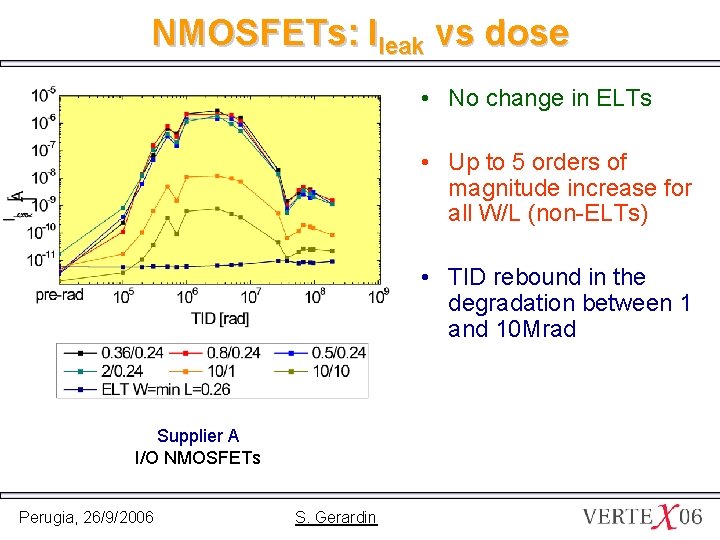
NMOSFETs: Ileak vs dose • No change in ELTs • Up to 5 orders of magnitude increase for all W/L (non-ELTs) • TID rebound in the degradation between 1 and 10 Mrad Supplier A I/O NMOSFETs Perugia, 26/9/2006 S. Gerardin

PMOSFETs: DVth vs dose • DVth up to 350 m. V in minimum-size devices • Smaller dependence on geometry than NMOSFETs • Monotonic increase Supplier A I/O PMOSFETs Perugia, 26/9/2006 S. Gerardin

Impact of Bias and Foundry • Bias: dependence similar to that of core transistors – DVth. max(MS NMOSFETs) from -50 m. V to -250 m. V – Ileak, max(NMOSFETs) ↑ from 10 x to 105 x • Foundry: variability similar to that of core transistors – DVth, max(NMOSFETs) from -400 m. V to -60 m. V – Ileak, max(NMOSFETs) ↑ from 102 x to 108 x Perugia, 26/9/2006 S. Gerardin

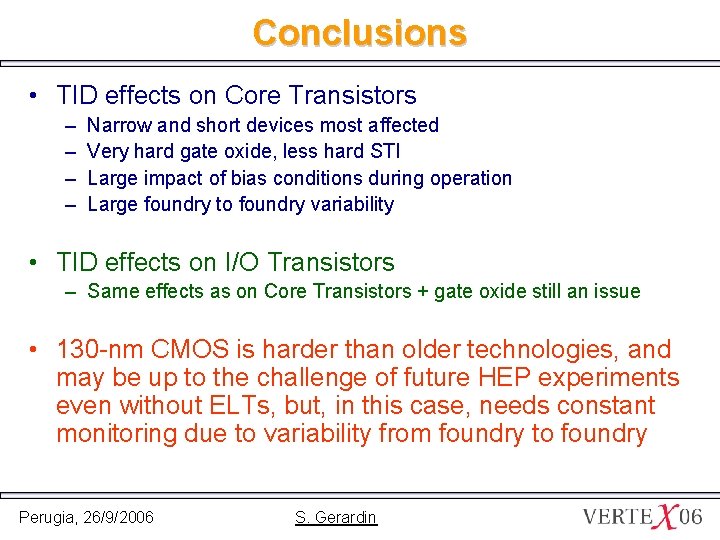
Conclusions • TID effects on Core Transistors – – Narrow and short devices most affected Very hard gate oxide, less hard STI Large impact of bias conditions during operation Large foundry to foundry variability • TID effects on I/O Transistors – Same effects as on Core Transistors + gate oxide still an issue • 130 -nm CMOS is harder than older technologies, and may be up to the challenge of future HEP experiments even without ELTs, but, in this case, needs constant monitoring due to variability from foundry to foundry Perugia, 26/9/2006 S. Gerardin

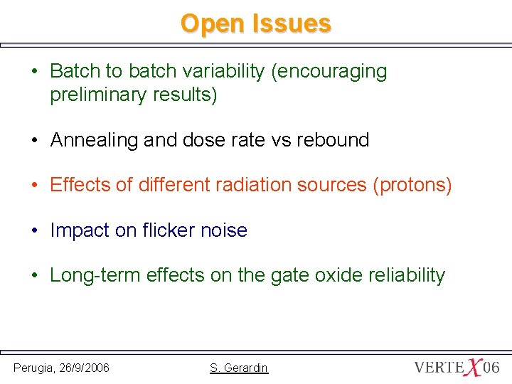
Open Issues • Batch to batch variability (encouraging preliminary results) • Annealing and dose rate vs rebound • Effects of different radiation sources (protons) • Impact on flicker noise • Long-term effects on the gate oxide reliability Perugia, 26/9/2006 S. Gerardin