Topological Insulators Their Spintronics Application Xuesen Wang National
![[111] Covalent bond Bi(111) bilayer: a 2 D Spin Hall Insulator } c a [111] Covalent bond Bi(111) bilayer: a 2 D Spin Hall Insulator } c a](https://slidetodoc.com/presentation_image_h/3429939962d874afe96e5615453dff63/image-18.jpg)
- Slides: 48

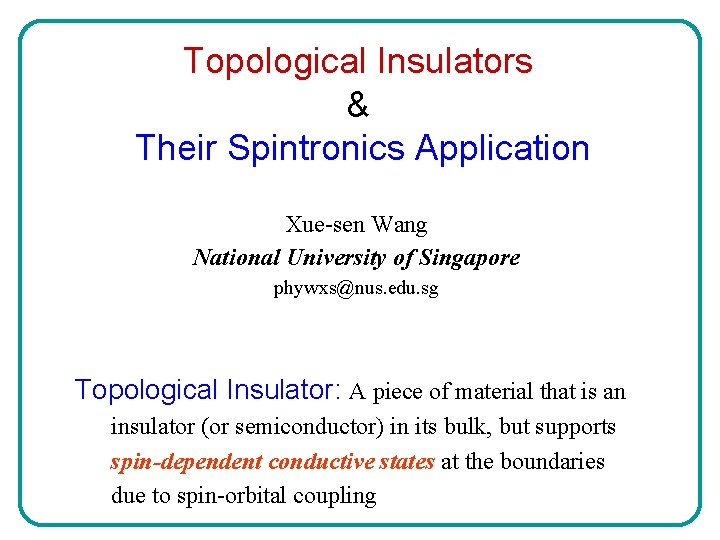
Topological Insulators & Their Spintronics Application Xue-sen Wang National University of Singapore phywxs@nus. edu. sg Topological Insulator: A piece of material that is an insulator (or semiconductor) in its bulk, but supports spin-dependent conductive states at the boundaries due to spin-orbital coupling

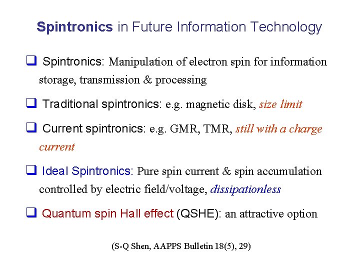
Spintronics in Future Information Technology q Spintronics: Manipulation of electron spin for information storage, transmission & processing q Traditional spintronics: e. g. magnetic disk, size limit q Current spintronics: e. g. GMR, TMR, still with a charge current q Ideal Spintronics: Pure spin current & spin accumulation controlled by electric field/voltage, dissipationless q Quantum spin Hall effect (QSHE): an attractive option (S-Q Shen, AAPPS Bulletin 18(5), 29)

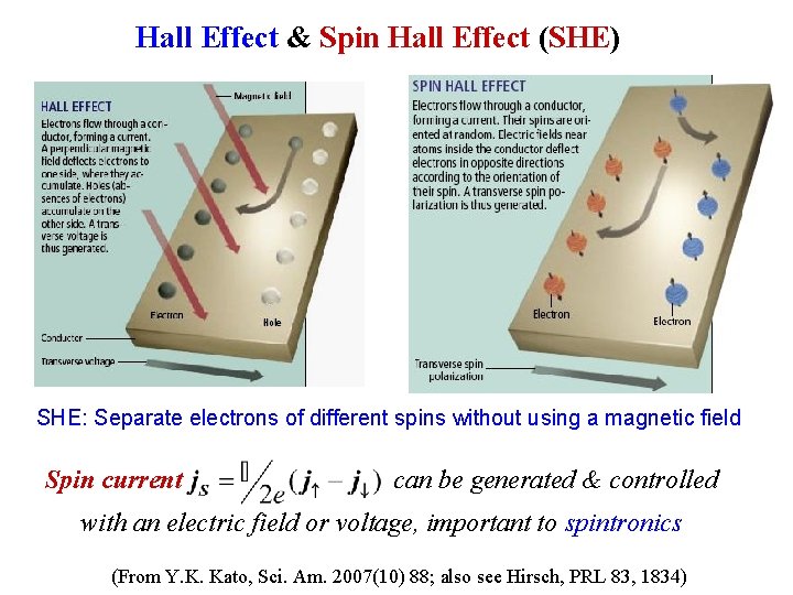
Hall Effect & Spin Hall Effect (SHE) SHE: Separate electrons of different spins without using a magnetic field Spin current can be generated & controlled with an electric field or voltage, important to spintronics (From Y. K. Kato, Sci. Am. 2007(10) 88; also see Hirsch, PRL 83, 1834)

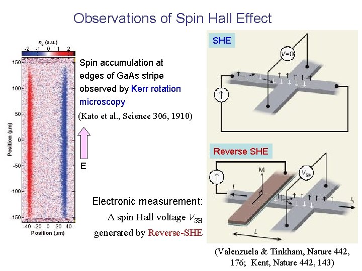
Observations of Spin Hall Effect SHE Spin accumulation at edges of Ga. As stripe observed by Kerr rotation microscopy (Kato et al. , Science 306, 1910) Reverse SHE E Electronic measurement: A spin Hall voltage VSH generated by Reverse-SHE (Valenzuela & Tinkham, Nature 442, 176; Kent, Nature 442, 143)

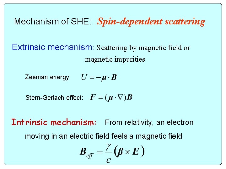
Mechanism of SHE: Spin-dependent scattering Extrinsic mechanism: Scattering by magnetic field or magnetic impurities Zeeman energy: Stern-Gerlach effect: Intrinsic mechanism: From relativity, an electron moving in an electric field feels a magnetic field

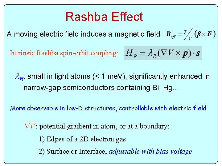
Rashba Effect A moving electric field induces a magnetic field: Intrinsic Rashba spin-orbit coupling: R: small in light atoms (< 1 me. V), significantly enhanced in narrow-gap semiconductors containing Bi, Hg… More observable in low-D structures, controllable with electric field V: potential gradient in atom, or at a boundary: 1) Edges of a 2 D electron gas 2) Surface or Interface, adjustable with bias voltage

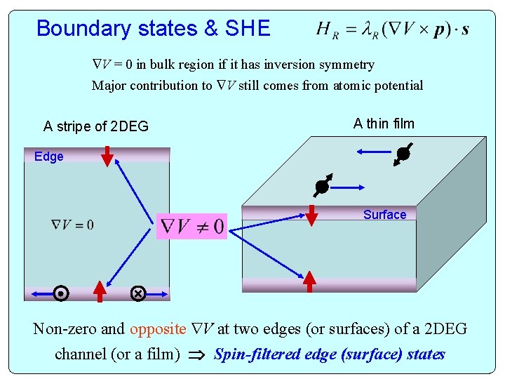
Boundary states & SHE V = 0 in bulk region if it has inversion symmetry Major contribution to V still comes from atomic potential A stripe of 2 DEG A thin film Edge Surface × Non-zero and opposite V at two edges (or surfaces) of a 2 DEG channel (or a film) Spin-filtered edge (surface) states

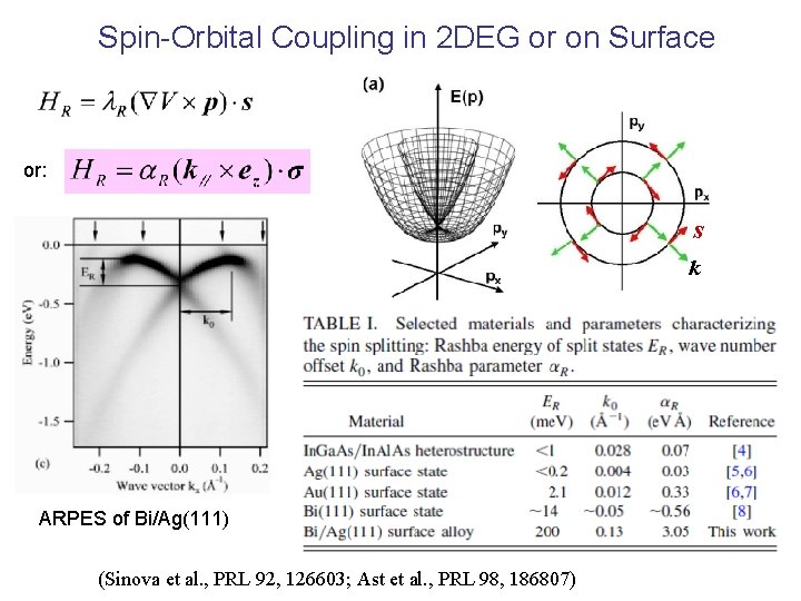
Spin-Orbital Coupling in 2 DEG or on Surface or: s k ARPES of Bi/Ag(111) (Sinova et al. , PRL 92, 126603; Ast et al. , PRL 98, 186807)

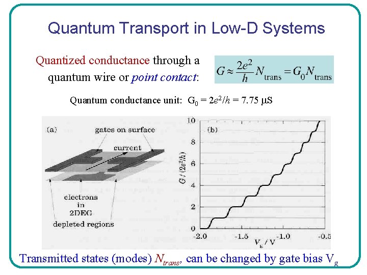
Quantum Transport in Low-D Systems Quantized conductance through a quantum wire or point contact: Quantum conductance unit: G 0 = 2 e 2/h = 7. 75 S Transmitted states (modes) Ntrans, can be changed by gate bias Vg

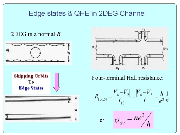
Edge states & QHE in 2 DEG Channel 2 DEG in a normal B Skipping Orbits To Edge States Four-terminal Hall resistance: or:

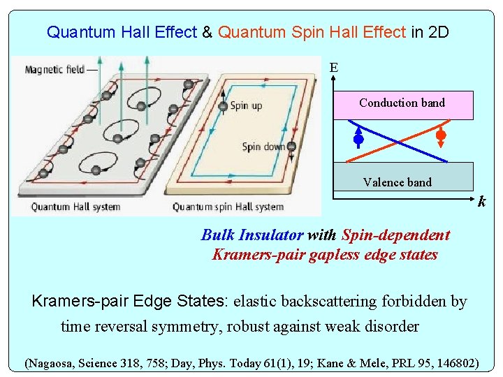
Quantum Hall Effect & Quantum Spin Hall Effect in 2 D E Conduction band Valence band k Bulk Insulator with Spin-dependent Kramers-pair gapless edge states Kramers-pair Edge States: elastic backscattering forbidden by time reversal symmetry, robust against weak disorder (Nagaosa, Science 318, 758; Day, Phys. Today 61(1), 19; Kane & Mele, PRL 95, 146802)

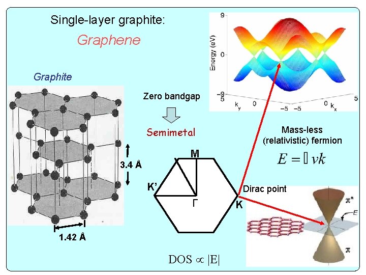
Single-layer graphite: Graphene Graphite Zero bandgap Mass-less (relativistic) fermion Semimetal M 3. 4 Å K’ Dirac point Γ 1. 42 Å DOS |E| K

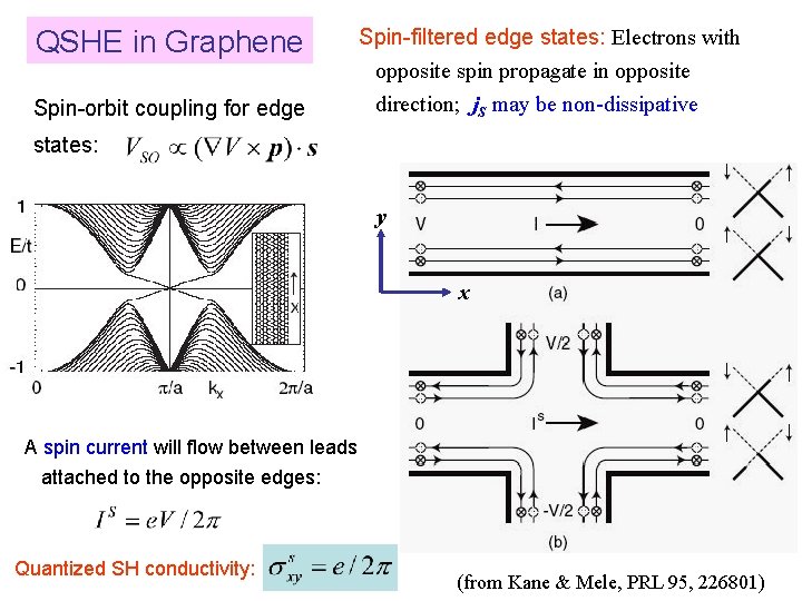
QSHE in Graphene Spin-orbit coupling for edge Spin-filtered edge states: Electrons with opposite spin propagate in opposite direction; j. S may be non-dissipative states: y x A spin current will flow between leads attached to the opposite edges: Quantized SH conductivity: (from Kane & Mele, PRL 95, 226801)

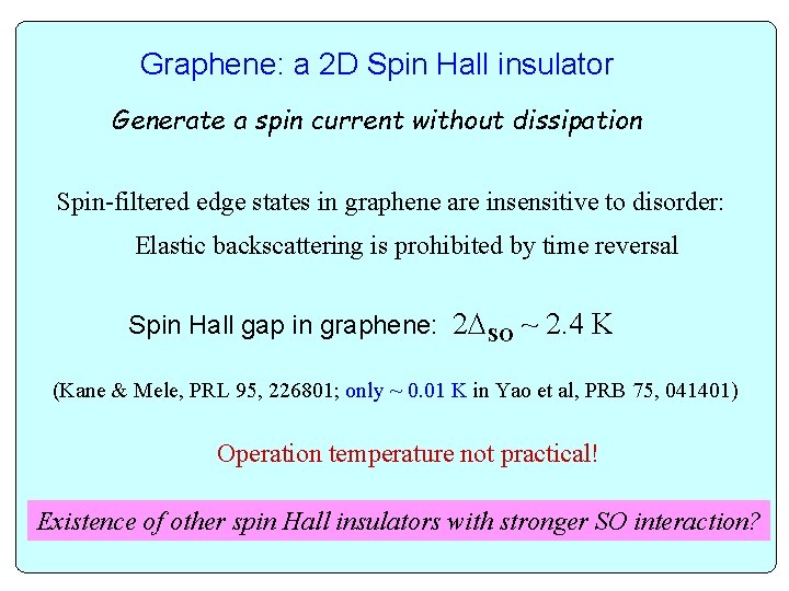
Graphene: a 2 D Spin Hall insulator Generate a spin current without dissipation Spin-filtered edge states in graphene are insensitive to disorder: Elastic backscattering is prohibited by time reversal Spin Hall gap in graphene: 2 SO ~ 2. 4 K (Kane & Mele, PRL 95, 226801; only ~ 0. 01 K in Yao et al, PRB 75, 041401) Operation temperature not practical! Existence of other spin Hall insulators with stronger SO interaction?

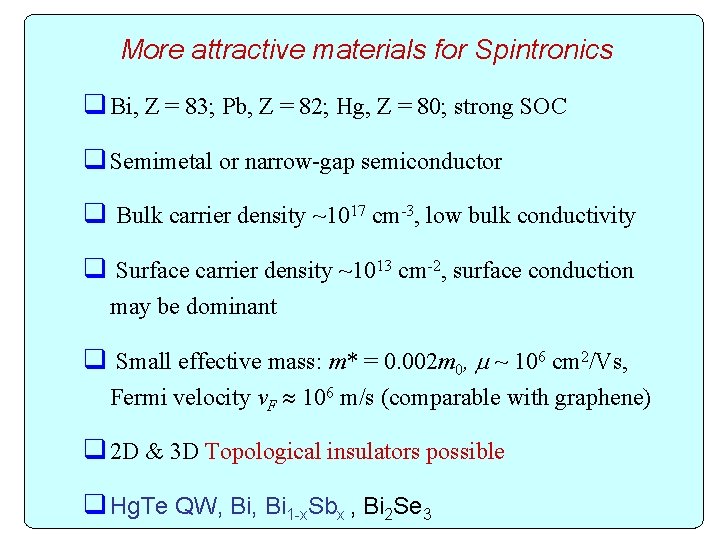
More attractive materials for Spintronics q Bi, Z = 83; Pb, Z = 82; Hg, Z = 80; strong SOC q Semimetal or narrow-gap semiconductor q Bulk carrier density ~1017 cm-3, low bulk conductivity q Surface carrier density ~1013 cm-2, surface conduction may be dominant q Small effective mass: m* = 0. 002 m 0, ~ 106 cm 2/Vs, Fermi velocity v. F 106 m/s (comparable with graphene) q 2 D & 3 D Topological insulators possible q Hg. Te QW, Bi 1 -x. Sbx , Bi 2 Se 3

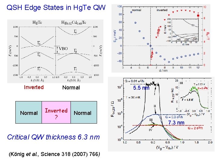
QSH Edge States in Hg. Te QW Inverted Normal Inverted ? 5. 5 nm Normal Critical QW thickness 6. 3 nm (König et al. , Science 318 (2007) 766) 7. 3 nm

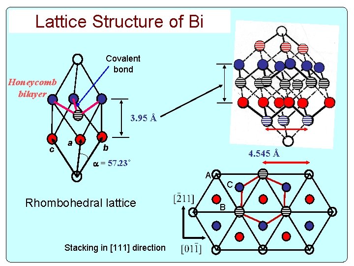
Lattice Structure of Bi Covalent bond Honeycomb bilayer 3. 95 Å c a b 4. 545 Å = 57. 23˚ A Rhombohedral lattice Stacking in [111] direction C B
![111 Covalent bond Bi111 bilayer a 2 D Spin Hall Insulator c a [111] Covalent bond Bi(111) bilayer: a 2 D Spin Hall Insulator } c a](https://slidetodoc.com/presentation_image_h/3429939962d874afe96e5615453dff63/image-18.jpg)
[111] Covalent bond Bi(111) bilayer: a 2 D Spin Hall Insulator } c a 2 D bandgap 0. 2 e. V 1 Kramers pair of edge states b Honeycomb bilayer Spin Hall Conductivity: (Murakami, PRL 97, 236805; Liu et al. , PRB 76, 121301)

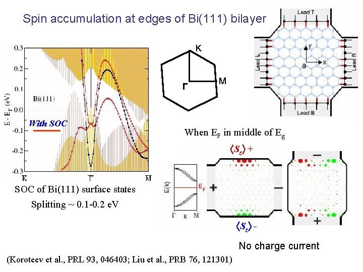
Spin accumulation at edges of Bi(111) bilayer K Γ With SOC M When EF in middle of Eg Sz + SOC of Bi(111) surface states Splitting ~ 0. 1 -0. 2 e. V Sz No charge current (Koroteev et al. , PRL 93, 046403; Liu et al. , PRB 76, 121301)

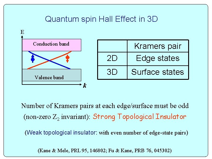
Quantum spin Hall Effect in 3 D E Conduction band Valence band 2 D Kramers pair Edge states 3 D Surface states k Number of Kramers pairs at each edge/surface must be odd (non-zero Z 2 invariant): Strong Topological Insulator (Weak topological insulator: with even number of edge-state pairs) (Kane & Mele, PRL 95, 146802; Fu & Kane, PRB 76, 045302)

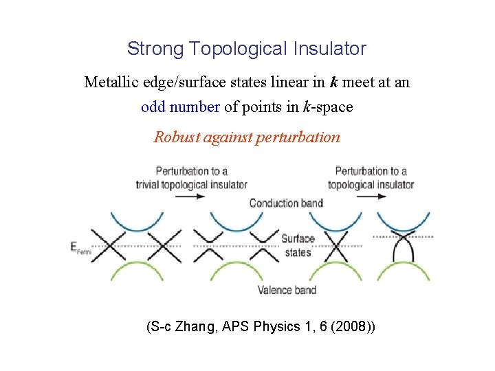
Strong Topological Insulator Metallic edge/surface states linear in k meet at an odd number of points in k-space Robust against perturbation (S-c Zhang, APS Physics 1, 6 (2008))

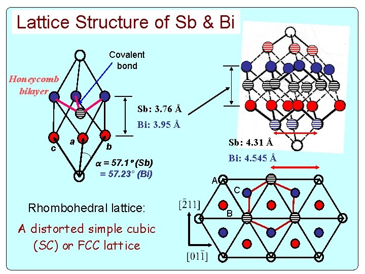
Lattice Structure of Sb & Bi Covalent bond Honeycomb bilayer Sb: 3. 76 Å Bi: 3. 95 Å c a Sb: 4. 31 Å b Bi: 4. 545 Å = 57. 1 (Sb) = 57. 23° (Bi) Rhombohedral lattice: A distorted simple cubic (SC) or FCC lattice A C B

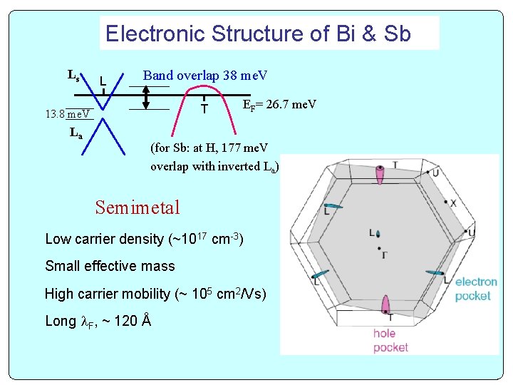
Electronic Structure of Bi & Sb Ls L Band overlap 38 me. V T 13. 8 me. V La EF= 26. 7 me. V (for Sb: at H, 177 me. V overlap with inverted La) Semimetal Low carrier density (~1017 cm-3) Small effective mass High carrier mobility (~ 105 cm 2/Vs) Long F, ~ 120 Å

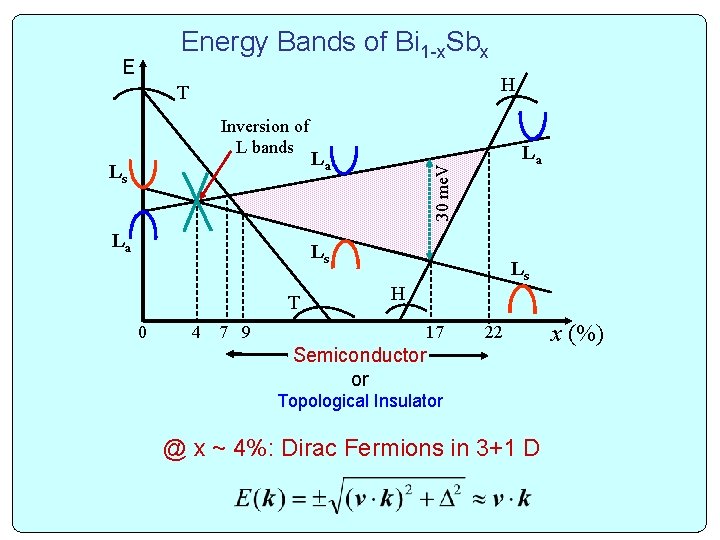
Energy Bands of Bi 1 -x. Sbx E H T Ls La La La 30 me. V Inversion of L bands Ls T 0 4 Ls H 7 9 17 22 Semiconductor or Topological Insulator @ x ~ 4%: Dirac Fermions in 3+1 D x (%)

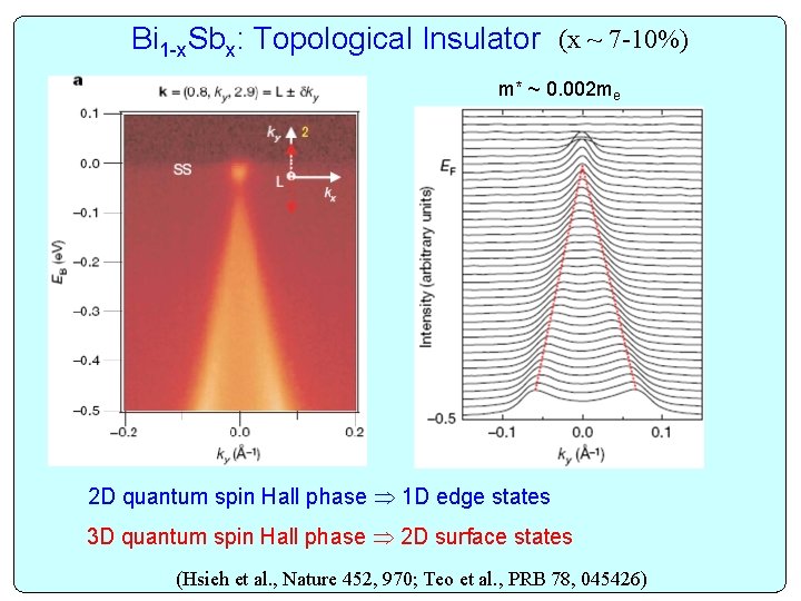
Bi 1 -x. Sbx: Topological Insulator (x ~ 7 -10%) m* ~ 0. 002 me 2 D quantum spin Hall phase 1 D edge states 3 D quantum spin Hall phase 2 D surface states (Hsieh et al. , Nature 452, 970; Teo et al. , PRB 78, 045426)

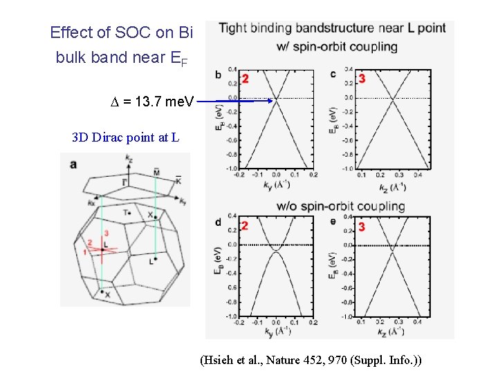
Effect of SOC on Bi bulk band near EF = 13. 7 me. V 3 D Dirac point at L (Hsieh et al. , Nature 452, 970 (Suppl. Info. ))

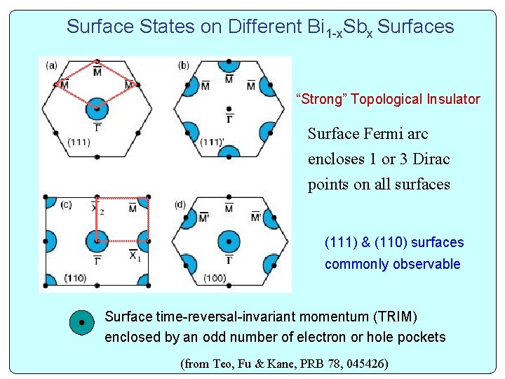
Surface States on Different Bi 1 -x. Sbx Surfaces “Strong” Topological Insulator Surface Fermi arc encloses 1 or 3 Dirac points on all surfaces (111) & (110) surfaces commonly observable Surface time-reversal-invariant momentum (TRIM) enclosed by an odd number of electron or hole pockets (from Teo, Fu & Kane, PRB 78, 045426)

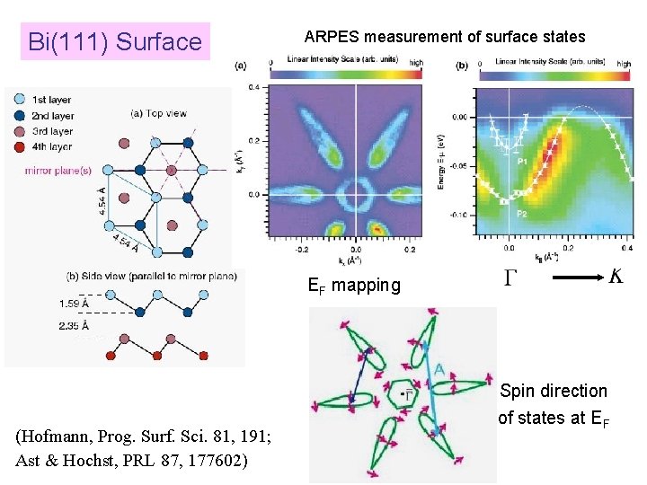
Bi(111) Surface ARPES measurement of surface states EF mapping (Hofmann, Prog. Surf. Sci. 81, 191; Ast & Hochst, PRL 87, 177602) Spin direction of states at EF

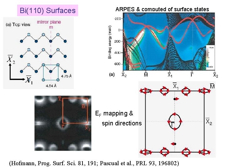
Bi(110) Surfaces ARPES & computed of surface states EF mapping & spin directions (Hofmann, Prog. Surf. Sci. 81, 191; Pascual et al. , PRL 93, 196802)

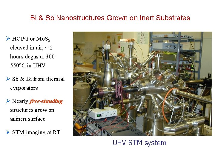
Bi & Sb Nanostructures Grown on Inert Substrates Ø HOPG or Mo. S 2 cleaved in air, ~ 5 hours degas at 300550 C in UHV Ø Sb & Bi from thermal evaporators Ø Nearly free-standing structures grow on aninert surface Ø STM imaging at RT UHV STM system

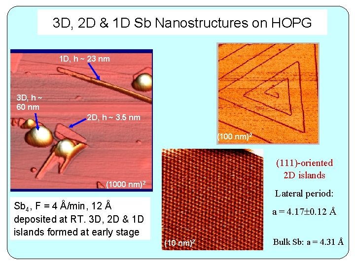
3 D, 2 D & 1 D Sb Nanostructures on HOPG 1 D, h ~ 23 nm 3 D, h ~ 60 nm 2 D, h ~ 3. 5 nm (100 nm)2 (111)-oriented 2 D islands (1000 nm)2 Lateral period: Sb 4, F = 4 Å/min, 12 Å deposited at RT. 3 D, 2 D & 1 D islands formed at early stage a = 4. 17 0. 12 Å (10 nm)2 Bulk Sb: a = 4. 31 Å

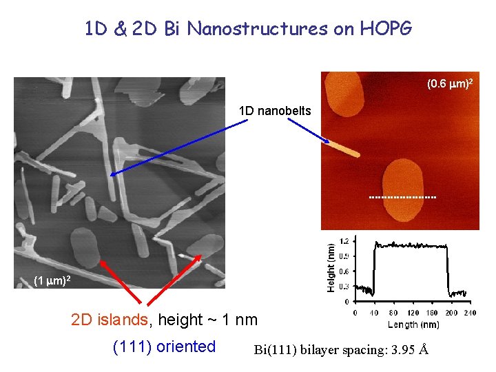
1 D & 2 D Bi Nanostructures on HOPG (0. 6 m)2 1 D nanobelts (1 m)2 2 D islands, height ~ 1 nm (111) oriented Bi(111) bilayer spacing: 3. 95 Å

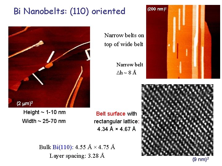
Bi Nanobelts: (110) oriented (200 nm)2 Narrow belts on top of wide belt Narrow belt h ~ 8 Å (2 m)2 Height ~ 1 -10 nm Width ~ 25 -70 nm Belt surface with rectangular lattice: 4. 34 Å × 4. 67 Å Bulk Bi(110): 4. 55 Å × 4. 75 Å Layer spacing: 3. 28 Å (9 nm)2

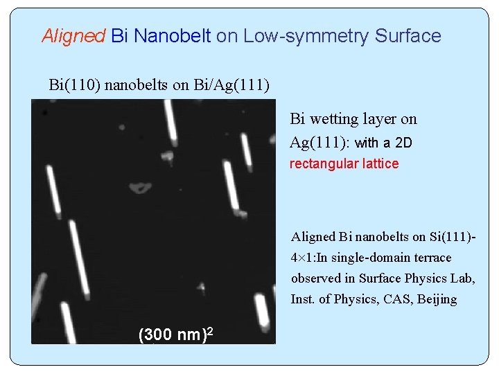
Aligned Bi Nanobelt on Low-symmetry Surface Bi(110) nanobelts on Bi/Ag(111) Bi wetting layer on Ag(111): with a 2 D rectangular lattice Aligned Bi nanobelts on Si(111)4 1: In single-domain terrace observed in Surface Physics Lab, Inst. of Physics, CAS, Beijing (300 nm)2

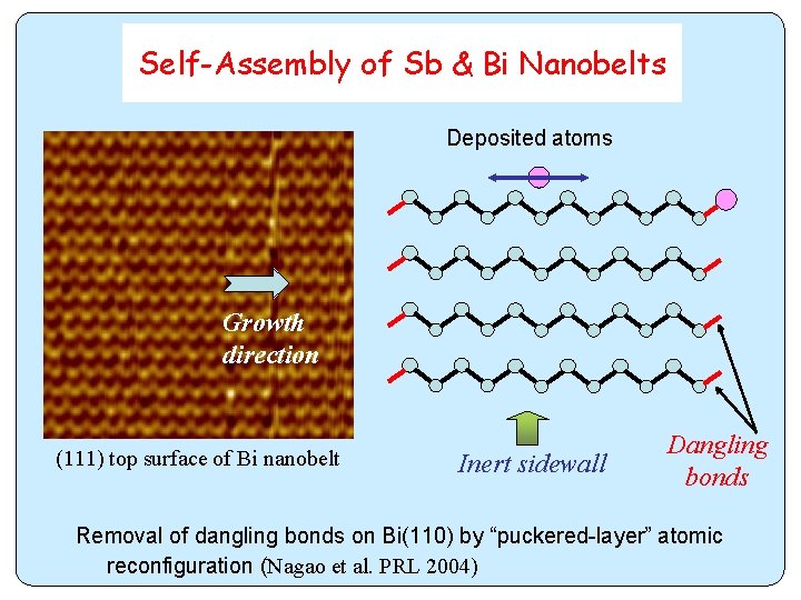
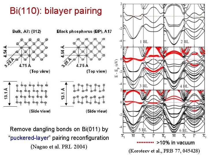
Self-Assembly of Sb & Bi Nanobelts Deposited atoms Growth direction (111) top surface of Bi nanobelt Inert sidewall Dangling bonds Removal of dangling bonds on Bi(110) by “puckered-layer” atomic reconfiguration (Nagao et al. PRL 2004)

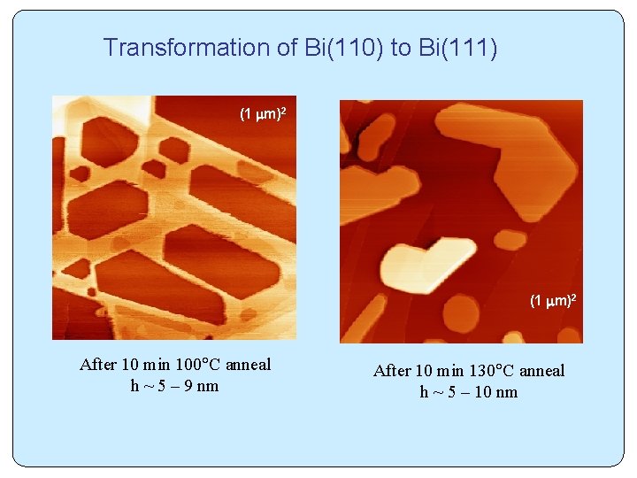
Transformation of Bi(110) to Bi(111) (1 m)2 After 10 min 100 C anneal h ~ 5 – 9 nm After 10 min 130 C anneal h ~ 5 – 10 nm

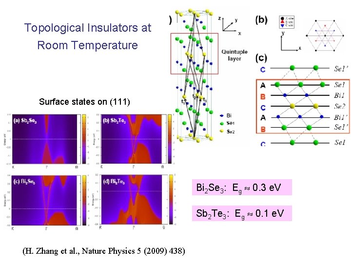
Topological Insulators at Room Temperature Surface states on (111) Bi 2 Se 3: Eg 0. 3 e. V Sb 2 Te 3: Eg 0. 1 e. V (H. Zhang et al. , Nature Physics 5 (2009) 438)

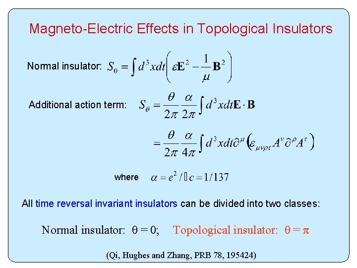
Magneto-Electric Effects in Topological Insulators Normal insulator: Additional action term: where All time reversal invariant insulators can be divided into two classes: Normal insulator: θ = 0; Topological insulator: θ = π (Qi, Hughes and Zhang, PRB 78, 195424)

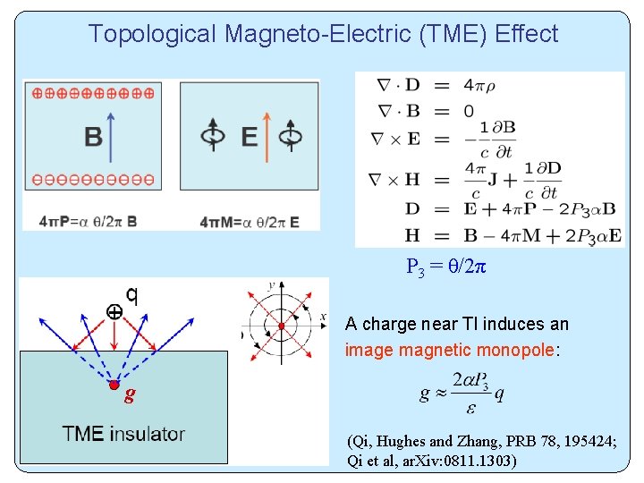
Topological Magneto-Electric (TME) Effect P 3 = θ/2π A charge near TI induces an image magnetic monopole: g (Qi, Hughes and Zhang, PRB 78, 195424; Qi et al, ar. Xiv: 0811. 1303)

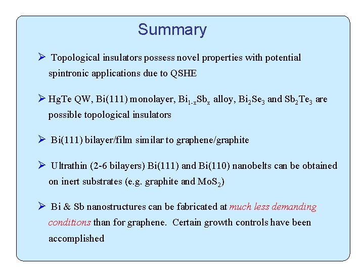
Summary Ø Topological insulators possess novel properties with potential spintronic applications due to QSHE Ø Hg. Te QW, Bi(111) monolayer, Bi 1 -x. Sbx alloy, Bi 2 Se 3 and Sb 2 Te 3 are possible topological insulators Ø Bi(111) bilayer/film similar to graphene/graphite Ø Ultrathin (2 -6 bilayers) Bi(111) and Bi(110) nanobelts can be obtained on inert substrates (e. g. graphite and Mo. S 2) Ø Bi & Sb nanostructures can be fabricated at much less demanding conditions than for graphene. Certain growth controls have been accomplished

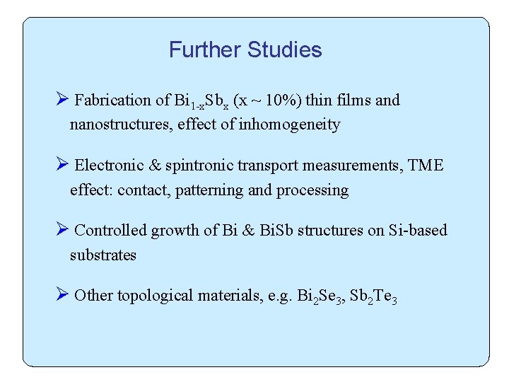
Further Studies Ø Fabrication of Bi 1 -x. Sbx (x ~ 10%) thin films and nanostructures, effect of inhomogeneity Ø Electronic & spintronic transport measurements, TME effect: contact, patterning and processing Ø Controlled growth of Bi & Bi. Sb structures on Si-based substrates Ø Other topological materials, e. g. Bi 2 Se 3, Sb 2 Te 3

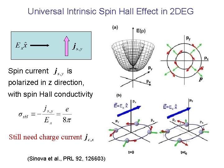
Universal Intrinsic Spin Hall Effect in 2 DEG Spin current is polarized in z direction, with spin Hall conductivity Still need charge current (Sinova et al. , PRL 92, 126603) s p

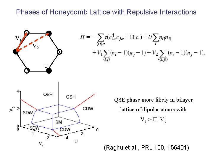
Phases of Honeycomb Lattice with Repulsive Interactions V 1 V 2 U QSE phase more likely in bilayer lattice of dipolar atoms with V 2 > U, V 1 (Raghu et al. , PRL 100, 156401)

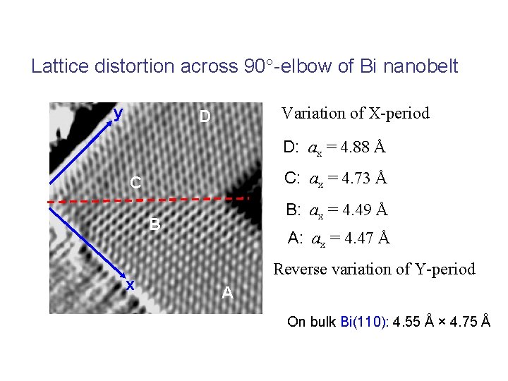
Lattice distortion across 90 -elbow of Bi nanobelt y Variation of X-period D D: ax = 4. 88 Å C: ax = 4. 73 Å C B: ax = 4. 49 Å B x A: ax = 4. 47 Å Reverse variation of Y-period A On bulk Bi(110): 4. 55 Å × 4. 75 Å

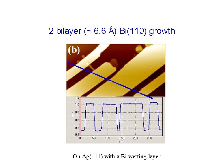
2 bilayer (~ 6. 6 Å) Bi(110) growth On Ag(111) with a Bi wetting layer

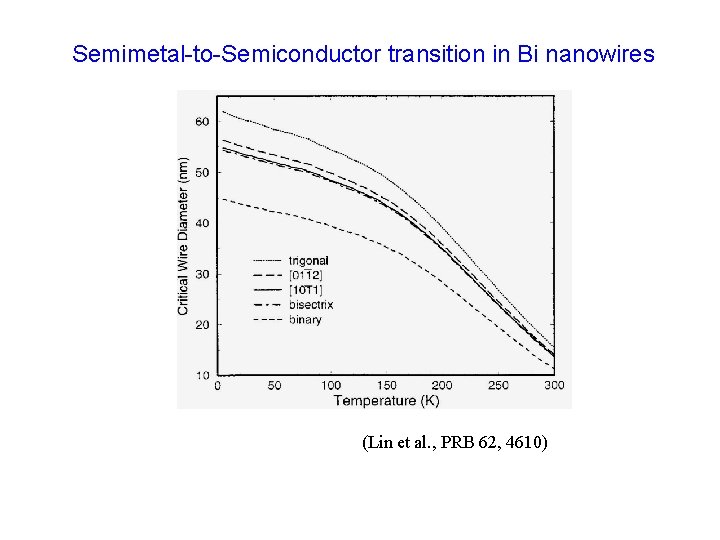
Semimetal-to-Semiconductor transition in Bi nanowires (Lin et al. , PRB 62, 4610)

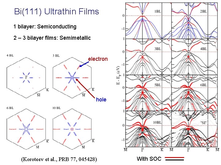
Bi(111) Ultrathin Films 1 bilayer: Semiconducting 2 – 3 bilayer films: Semimetallic electron hole (Koroteev et al. , PRB 77, 045428) With SOC

Bi(110): bilayer pairing Remove dangling bonds on Bi(011) by “puckered-layer” pairing reconfiguration (Nagao et al. PRL 2004) >10% in vacuum (Koroteev et al. , PRB 77, 045428)