Topics Latches and flipflops n RAMs and ROMs
- Slides: 34

Topics Latches and flip-flops. n RAMs and ROMs. n FPGA-Based System Design: Chapter 3 Copyright 2004 Prentice Hall PTR

Register Stores a value as controlled by clock. n May have load signal, etc. n In CMOS, memory is created by: n – capacitance (dynamic); – feedback (static). FPGA-Based System Design: Chapter 3 Copyright 2004 Prentice Hall PTR

Variations in registers Form of required clock signal. n How behavior of data input around clock affects the stored value. n When the stored value is presented to the output. n Whethere is ever a combinational path from input to output. n FPGA-Based System Design: Chapter 3 Copyright 2004 Prentice Hall PTR

Register terminology Latch: transparent when internal memory is being set from input. n Flip-flop: not transparent—reading input and changing output are separate events. n FPGA-Based System Design: Chapter 3 Copyright 2004 Prentice Hall PTR

Clock terminology Clock edge: rising or falling transition. n Duty cycle: fraction of clock period for which clock is active (e. g. , for active-low clock, fraction of time clock is 0). n FPGA-Based System Design: Chapter 3 Copyright 2004 Prentice Hall PTR

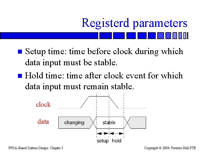
Registerd parameters Setup time: time before clock during which data input must be stable. n Hold time: time after clock event for which data input must remain stable. n clock data FPGA-Based System Design: Chapter 3 Copyright 2004 Prentice Hall PTR

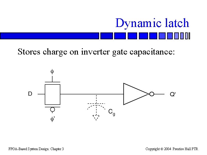
Dynamic latch Stores charge on inverter gate capacitance: FPGA-Based System Design: Chapter 3 Copyright 2004 Prentice Hall PTR

Latch characteristics Uses complementary transmission gate to ensure that storage node is always strongly driven. n Latch is transparent when transmission gate is closed. n Storage capacitance comes primarily from inverter gate capacitance. n FPGA-Based System Design: Chapter 3 Copyright 2004 Prentice Hall PTR

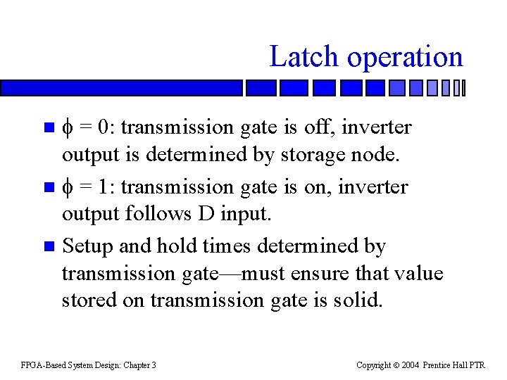
Latch operation = 0: transmission gate is off, inverter output is determined by storage node. n = 1: transmission gate is on, inverter output follows D input. n Setup and hold times determined by transmission gate—must ensure that value stored on transmission gate is solid. n FPGA-Based System Design: Chapter 3 Copyright 2004 Prentice Hall PTR

Stored charge leakage Stored charge leaks away due to reversebias leakage current. n Stored value is good for about 1 ms. n Value must be rewritten to be valid. n If not loaded every cycle, must ensure that latch is loaded often enough to keep data valid. n FPGA-Based System Design: Chapter 3 Copyright 2004 Prentice Hall PTR

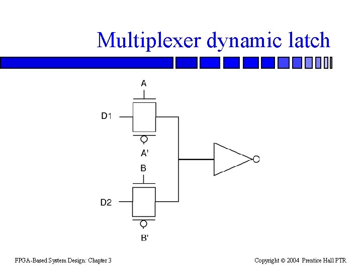
Multiplexer dynamic latch FPGA-Based System Design: Chapter 3 Copyright 2004 Prentice Hall PTR

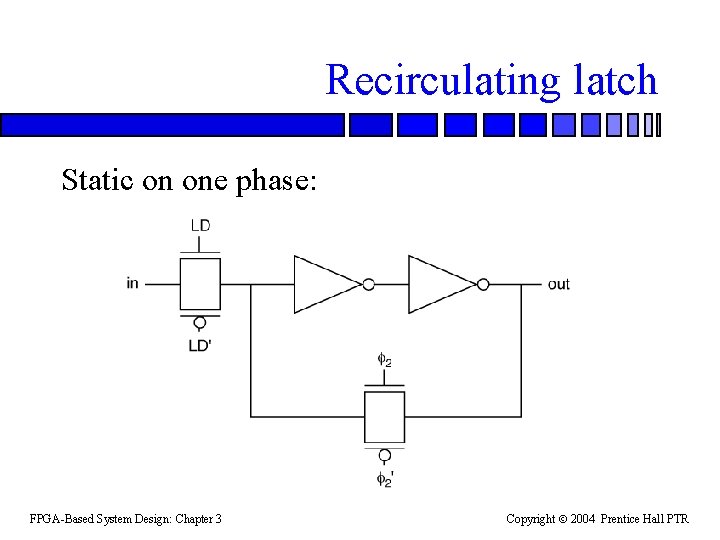
Non-dynamic latches Must use feedback to restore value. n Some latches are static on one phase (pseudo-static)—load on one phase, activate feedback on other phase. n FPGA-Based System Design: Chapter 3 Copyright 2004 Prentice Hall PTR

Recirculating latch Static on one phase: FPGA-Based System Design: Chapter 3 Copyright 2004 Prentice Hall PTR

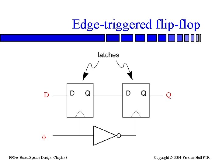
Edge-triggered flip-flop D Q FPGA-Based System Design: Chapter 3 Copyright 2004 Prentice Hall PTR

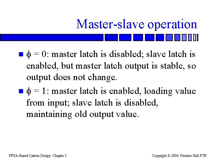
Master-slave operation = 0: master latch is disabled; slave latch is enabled, but master latch output is stable, so output does not change. n = 1: master latch is enabled, loading value from input; slave latch is disabled, maintaining old output value. n FPGA-Based System Design: Chapter 3 Copyright 2004 Prentice Hall PTR

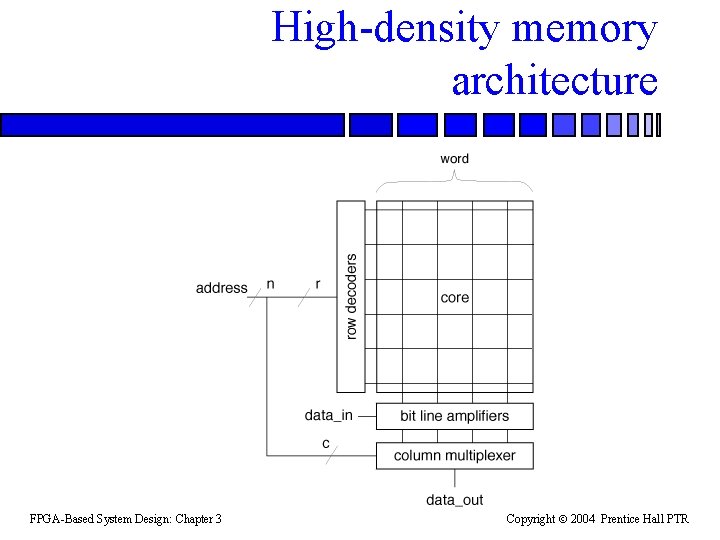
High-density memory architecture FPGA-Based System Design: Chapter 3 Copyright 2004 Prentice Hall PTR

Memory operation n Address is divided into row, column. – Row may contain full word or more than one word. Selected row drives/senses bit lines in columns. n Amplifiers/drivers read/write bit lines. n FPGA-Based System Design: Chapter 3 Copyright 2004 Prentice Hall PTR

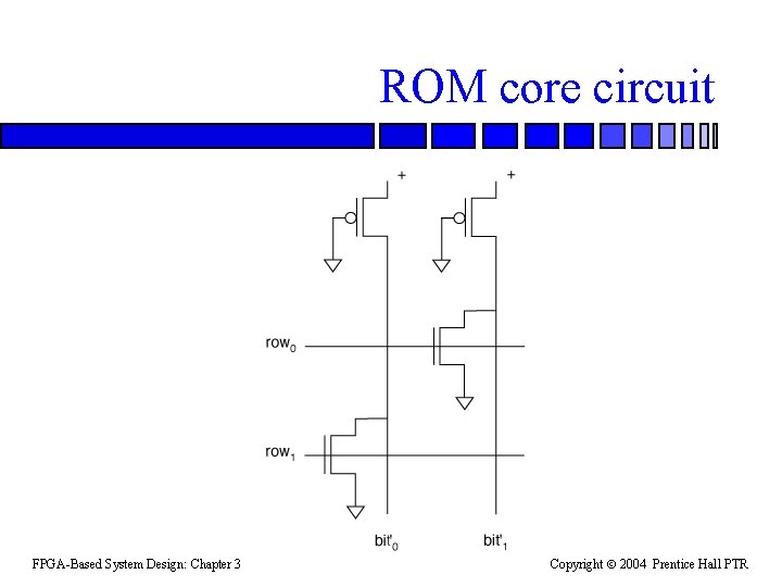
Read-only memory (ROM) ROM core is organized as NOR gates— pulldown transistors of NOR determine programming. n Mask-programmable ROM uses pulldowns to determine ROM contents. n FPGA-Based System Design: Chapter 3 Copyright 2004 Prentice Hall PTR

Flash memory Flash: electrically erasable PROM that can be programmed with standard voltages. n Uses dual capacitor structure. n Available in some digital processes for integrated memory, but raises the price of the manufacturing process. n FPGA-Based System Design: Chapter 3 Copyright 2004 Prentice Hall PTR

ROM core circuit FPGA-Based System Design: Chapter 3 Copyright 2004 Prentice Hall PTR

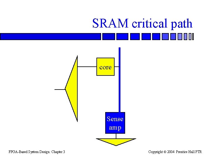
SRAM critical path core Sense amp FPGA-Based System Design: Chapter 3 Copyright 2004 Prentice Hall PTR

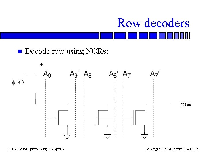
Row decoders n Decode row using NORs: FPGA-Based System Design: Chapter 3 Copyright 2004 Prentice Hall PTR

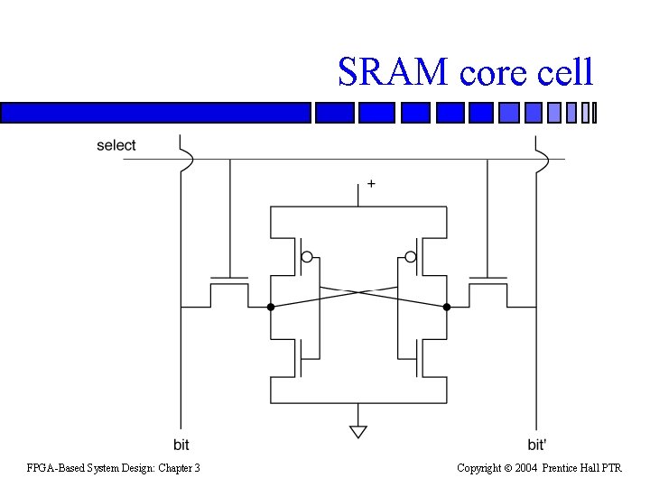
Static RAM (SRAM) Core cell uses six-transistor circuit to store value. n Value is stored symmetrically—both true and complement are stored on cross-coupled transistors. n SRAM retains value as long as power is applied to circuit. n FPGA-Based System Design: Chapter 3 Copyright 2004 Prentice Hall PTR

SRAM core cell FPGA-Based System Design: Chapter 3 Copyright 2004 Prentice Hall PTR

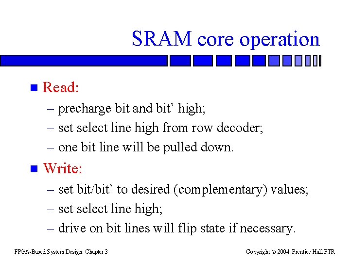
SRAM core operation n Read: – precharge bit and bit’ high; – set select line high from row decoder; – one bit line will be pulled down. n Write: – set bit/bit’ to desired (complementary) values; – set select line high; – drive on bit lines will flip state if necessary. FPGA-Based System Design: Chapter 3 Copyright 2004 Prentice Hall PTR

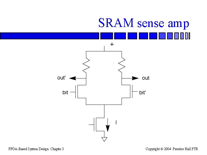
SRAM sense amp FPGA-Based System Design: Chapter 3 Copyright 2004 Prentice Hall PTR

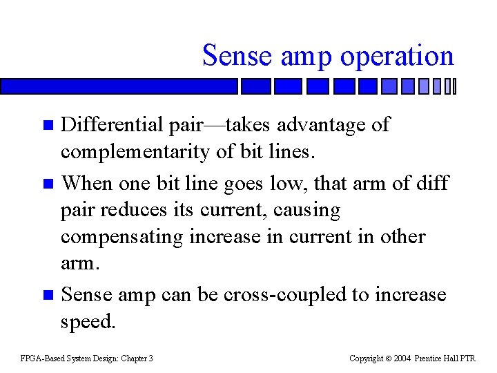
Sense amp operation Differential pair—takes advantage of complementarity of bit lines. n When one bit line goes low, that arm of diff pair reduces its current, causing compensating increase in current in other arm. n Sense amp can be cross-coupled to increase speed. n FPGA-Based System Design: Chapter 3 Copyright 2004 Prentice Hall PTR

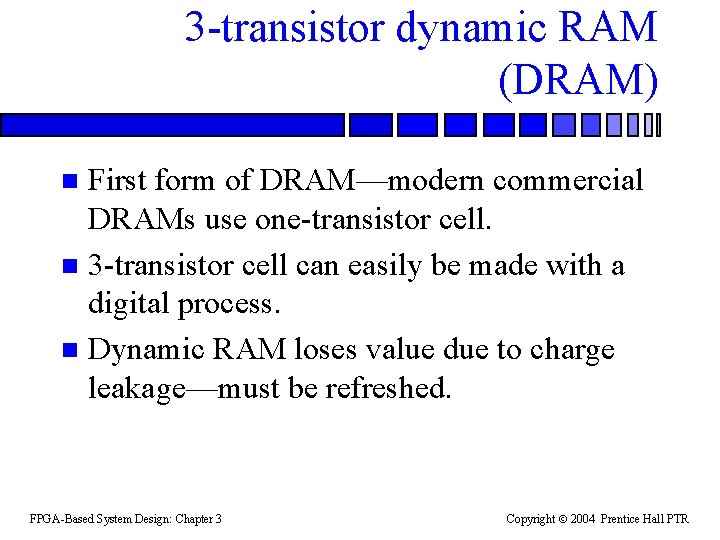
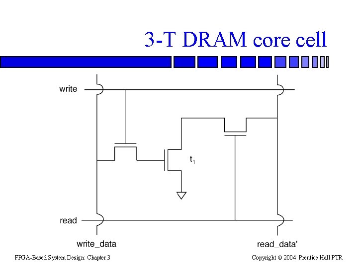
3 -transistor dynamic RAM (DRAM) First form of DRAM—modern commercial DRAMs use one-transistor cell. n 3 -transistor cell can easily be made with a digital process. n Dynamic RAM loses value due to charge leakage—must be refreshed. n FPGA-Based System Design: Chapter 3 Copyright 2004 Prentice Hall PTR

3 -T DRAM core cell FPGA-Based System Design: Chapter 3 Copyright 2004 Prentice Hall PTR

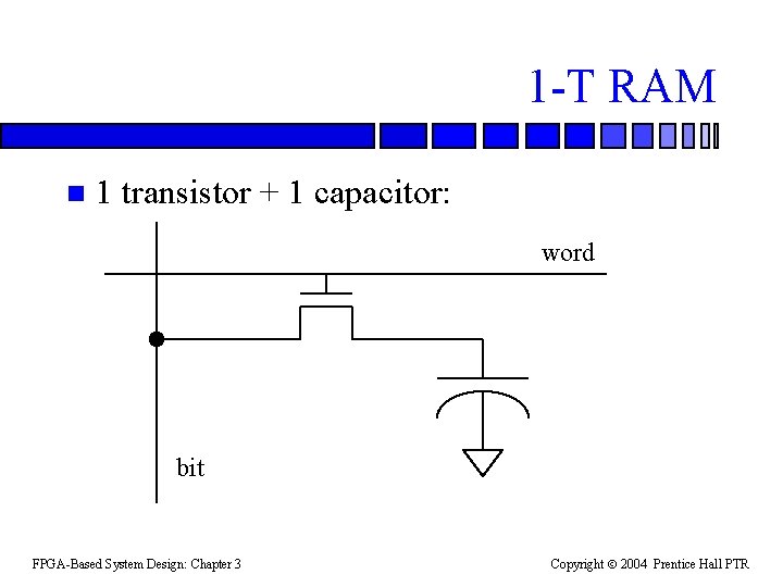
1 -T RAM n 1 transistor + 1 capacitor: word bit FPGA-Based System Design: Chapter 3 Copyright 2004 Prentice Hall PTR

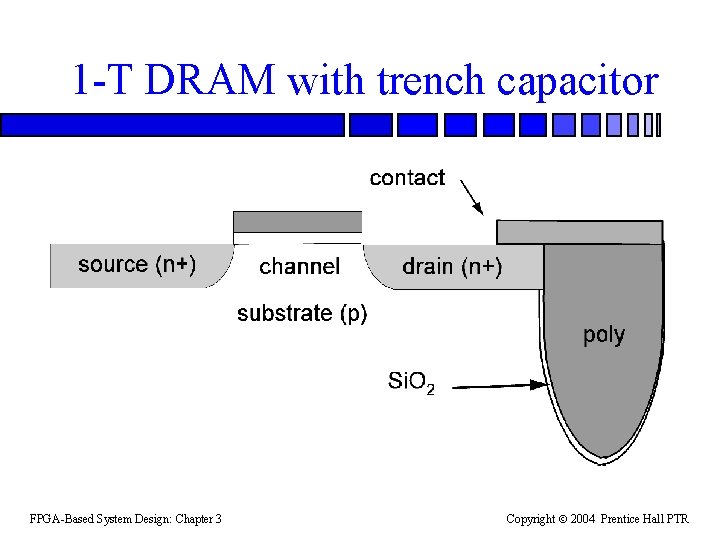
1 -T DRAM with trench capacitor FPGA-Based System Design: Chapter 3 Copyright 2004 Prentice Hall PTR

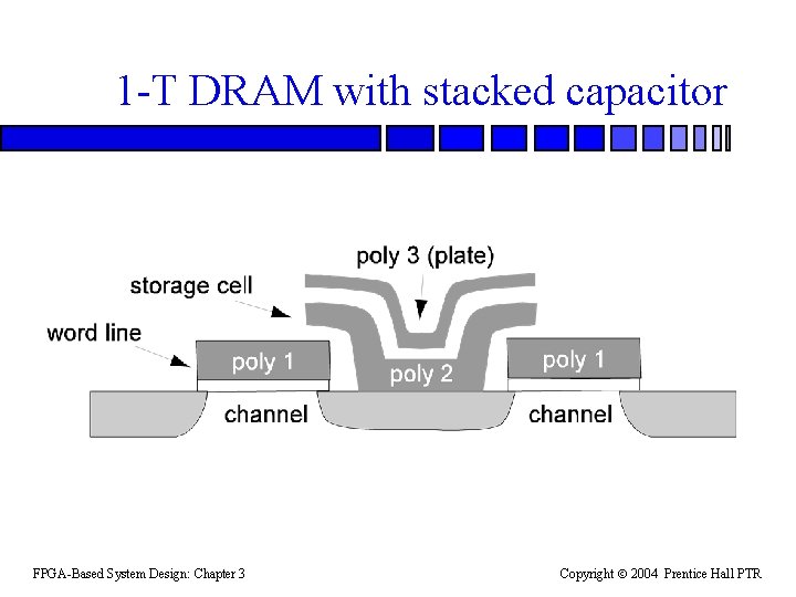
1 -T DRAM with stacked capacitor FPGA-Based System Design: Chapter 3 Copyright 2004 Prentice Hall PTR

Embedded DRAM is integrated with logic. n DRAM and logic processes are hard to make compatible. n – Capacitor requires high temperatures that destroy fine-line transistors. n Embedded DRAM is less dense than commodity DRAM. FPGA-Based System Design: Chapter 3 Copyright 2004 Prentice Hall PTR

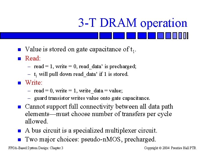
3 -T DRAM operation n n Value is stored on gate capacitance of t 1. Read: – read = 1, write = 0, read_data’ is precharged; – t 1 will pull down read_data’ if 1 is stored. n Write: – read = 0, write = 1, write_data = value; – guard transistor writes value onto gate capacitance. n n n Cannot support full connectivity between all data path elements—must choose number of transfers per cycle allowed. A bus circuit is a specialized multiplexer circuit. Two major choices: pseudo-n. MOS, precharged. FPGA-Based System Design: Chapter 3 Copyright 2004 Prentice Hall PTR