
Topics Design rules and fabrication n SCMOS scalable
Topics Design rules and fabrication. n SCMOS scalable design rules. n Stick diagrams. n Modern VLSI Design 3 e: Chapter 2 Copyright 1998, 2002 Prentice Hall PTR
Why we need design rules Masks are tooling for manufacturing. n Manufacturing processes have inherent limitations in accuracy. n Design rules specify geometry of masks which will provide reasonable yields. n Design rules are determined by experience. n Modern VLSI Design 3 e: Chapter 2 Copyright 1998, 2002 Prentice Hall PTR

Manufacturing problems Photoresist shrinkage, tearing. n Variations in material deposition. n Variations in temperature. n Variations in oxide thickness. n Impurities. n Variations between lots. n Variations across a wafer. n Modern VLSI Design 3 e: Chapter 2 Copyright 1998, 2002 Prentice Hall PTR
Transistor problems n Variations in threshold voltage: – oxide thickness; – ion implantation; – poly variations. Changes in source/drain diffusion overlap. n Variations in substrate. n Modern VLSI Design 3 e: Chapter 2 Copyright 1998, 2002 Prentice Hall PTR
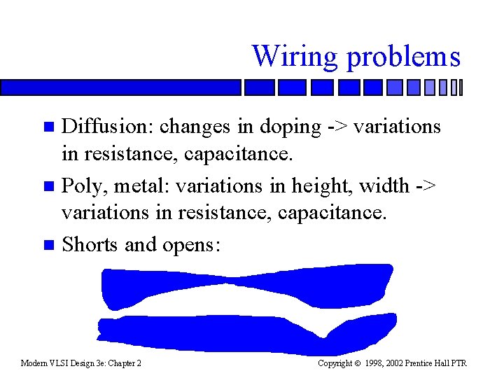
Wiring problems Diffusion: changes in doping -> variations in resistance, capacitance. n Poly, metal: variations in height, width -> variations in resistance, capacitance. n Shorts and opens: n Modern VLSI Design 3 e: Chapter 2 Copyright 1998, 2002 Prentice Hall PTR
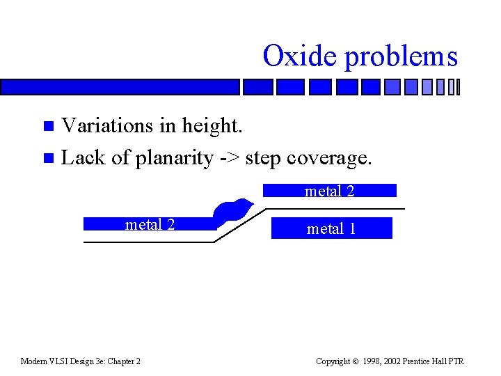
Oxide problems Variations in height. n Lack of planarity -> step coverage. n metal 2 Modern VLSI Design 3 e: Chapter 2 metal 1 Copyright 1998, 2002 Prentice Hall PTR
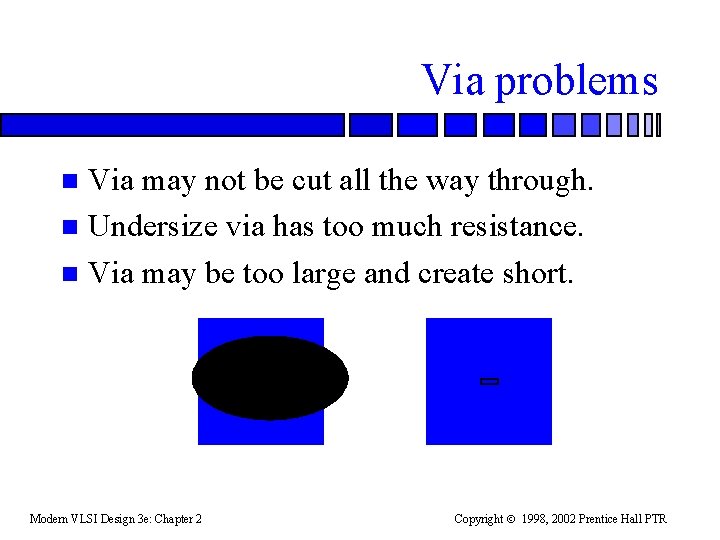
Via problems Via may not be cut all the way through. n Undersize via has too much resistance. n Via may be too large and create short. n Modern VLSI Design 3 e: Chapter 2 Copyright 1998, 2002 Prentice Hall PTR
MOSIS SCMOS design rules n n n Designed to scale across a wide range of technologies. Designed to support multiple vendors. Designed for educational use. Fairly conservative. http: //www. mosis. com/design/rules/ “The standard CMOS technology accessed by MOSIS is a single polysilicon, double metal, bulk CMOS process with enhancement-mode n -MOSFET and p-MOSFET devices”. Modern VLSI Design 3 e: Chapter 2 Copyright 1998, 2002 Prentice Hall PTR
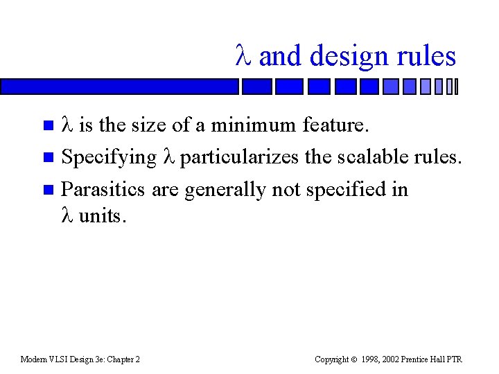
and design rules is the size of a minimum feature. n Specifying particularizes the scalable rules. n Parasitics are generally not specified in units n Modern VLSI Design 3 e: Chapter 2 Copyright 1998, 2002 Prentice Hall PTR
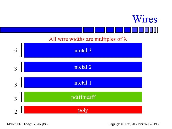
Wires All wire widths are multiples of 6 metal 3 3 metal 2 3 metal 1 3 pdiff/ndiff 2 poly Modern VLSI Design 3 e: Chapter 2 Copyright 1998, 2002 Prentice Hall PTR
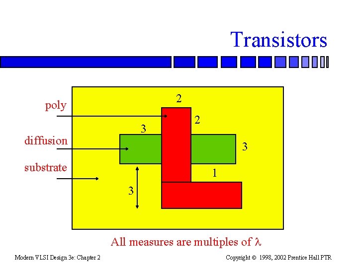
Transistors 2 poly 3 diffusion 2 3 substrate 1 3 All measures are multiples of Modern VLSI Design 3 e: Chapter 2 Copyright 1998, 2002 Prentice Hall PTR
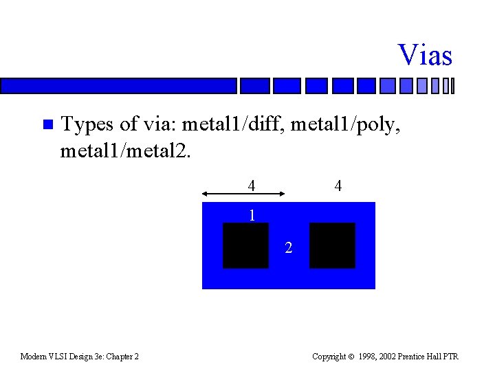
Vias n Types of via: metal 1/diff, metal 1/poly, metal 1/metal 2. 4 4 1 2 Modern VLSI Design 3 e: Chapter 2 Copyright 1998, 2002 Prentice Hall PTR
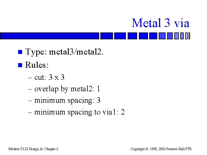
Metal 3 via Type: metal 3/metal 2. n Rules: n – cut: 3 x 3 – overlap by metal 2: 1 – minimum spacing: 3 – minimum spacing to via 1: 2 Modern VLSI Design 3 e: Chapter 2 Copyright 1998, 2002 Prentice Hall PTR
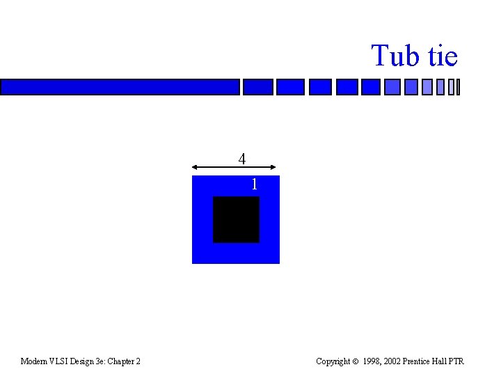
Tub tie 4 1 Modern VLSI Design 3 e: Chapter 2 Copyright 1998, 2002 Prentice Hall PTR
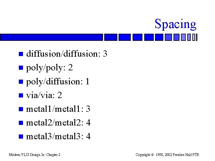
Spacing diffusion/diffusion: 3 n poly/poly: 2 n poly/diffusion: 1 n via/via: 2 n metal 1/metal 1: 3 n metal 2/metal 2: 4 n metal 3/metal 3: 4 n Modern VLSI Design 3 e: Chapter 2 Copyright 1998, 2002 Prentice Hall PTR
Overglass Cut in passivation layer. n Minimum bonding pad: 100 m. n Pad overlap of glass opening: 6 n Minimum pad spacing to unrelated metal 2 or metal 3: 30 n Minimum pad spacing to unrelated metal 1, poly, active: 15 n Modern VLSI Design 3 e: Chapter 2 Copyright 1998, 2002 Prentice Hall PTR
Stick diagrams A stick diagram is a cartoon of a layout. n Does show all components/vias (except possibly tub ties), relative placement. n Does not show exact placement, transistor sizes, wire lengths, wire widths, tub boundaries. n Modern VLSI Design 3 e: Chapter 2 Copyright 1998, 2002 Prentice Hall PTR
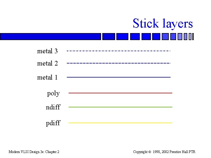
Stick layers metal 3 metal 2 metal 1 poly ndiff pdiff Modern VLSI Design 3 e: Chapter 2 Copyright 1998, 2002 Prentice Hall PTR
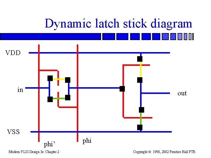
Dynamic latch stick diagram VDD in out VSS phi’ Modern VLSI Design 3 e: Chapter 2 phi Copyright 1998, 2002 Prentice Hall PTR
Sticks design of multiplexer n Start with NAND gate: Modern VLSI Design 3 e: Chapter 2 Copyright 1998, 2002 Prentice Hall PTR
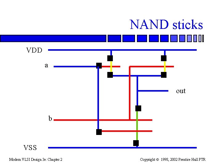
NAND sticks VDD a out b VSS Modern VLSI Design 3 e: Chapter 2 Copyright 1998, 2002 Prentice Hall PTR
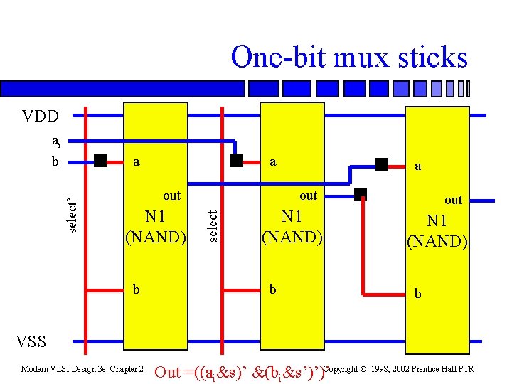
One-bit mux sticks VDD ai bi a out N 1 (NAND) b a out select’ a N 1 (NAND) b out N 1 (NAND) b VSS Modern VLSI Design 3 e: Chapter 2 Out =((ai&s)’ &(bi&s’)’)’Copyright 1998, 2002 Prentice Hall PTR
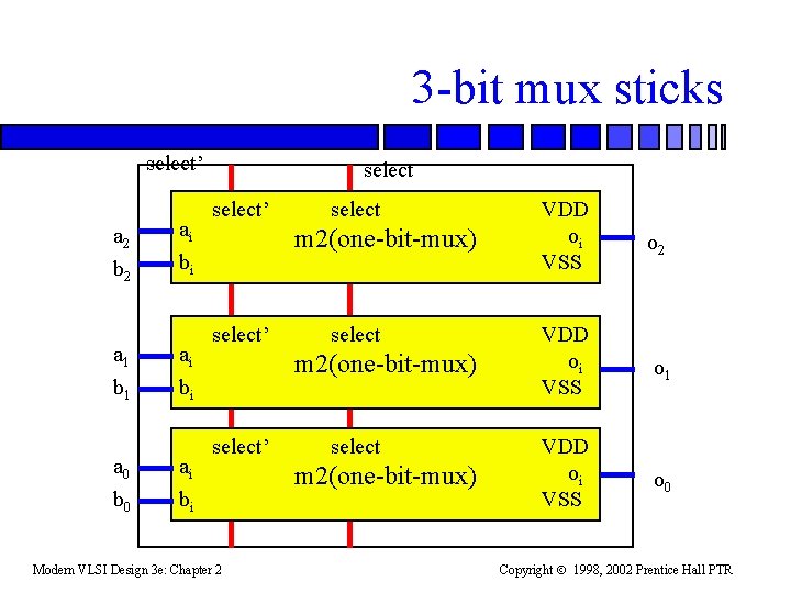
3 -bit mux sticks select’ a 2 b 2 a 1 b 1 a 0 b 0 ai bi select’ select m 2(one-bit-mux) select’ Modern VLSI Design 3 e: Chapter 2 select m 2(one-bit-mux) VDD oi VSS o 2 VDD oi VSS o 1 VDD oi VSS o 0 Copyright 1998, 2002 Prentice Hall PTR
Layout design and analysis tools Layout editors are interactive tools. n Design rule checkers are generally batch--identify DRC errors on the layout. n Circuit extractors extract the netlist from the layout. n Connectivity verification systems (CVS) compare extracted and original netlists. n Modern VLSI Design 3 e: Chapter 2 Copyright 1998, 2002 Prentice Hall PTR
Automatic layout Cell generators (macrocell generators) create optimized layouts for ALUs, etc. n Standard cell/sea-of-gates layout creates layout from predesigned cells + custom routing. n – Sea-of-gates allows routing over the cell. Modern VLSI Design 3 e: Chapter 2 Copyright 1998, 2002 Prentice Hall PTR
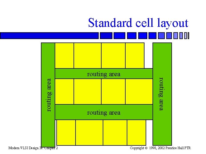
Standard cell layout Modern VLSI Design 3 e: Chapter 2 routing area Copyright 1998, 2002 Prentice Hall PTR
Homework Set 2 Problems 2 -1, 2 -2, 2 -3, 2. 10 (a), (b), pp. 103 -105, Textbook, Due, September 28, 2006. October -1: In problem 2. 10, use the side-wall capacitance as an estimate for the overhang capacitance for a 0. 5 micron process. Side-wall parasitic capacitance per micrometer is specified for both p and n type diffusion on page 85. The perimeter of the channel is given by 2(W+L). The bottom-wall parasitic capacitances for p and n type diffusions are also specified on page 85. Use the area (WL) to find the total bottom-wall capacitance of the source/drain region. The total capacity is found by adding the two together. Modern VLSI Design 3 e: Chapter 2 Copyright 1998, 2002 Prentice Hall PTR
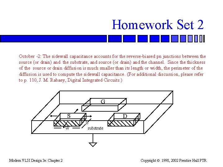
Homework Set 2 October -2: The sidewall capacitance accounts for the reverse-biased pn junctions between the source (or drain) and the substrate, and source (or drain) and the channel. Since thickness of the source or drain diffusion is much smaller than its length or width, the perimeter of the diffusion is used to compute the sidewall capacitance. (For additional discussion, please refer to p. 110, J. M. Rabaey, Digital Integrated Circuits. ) G S W Modern VLSI Design 3 e: Chapter 2 D L substrate Copyright 1998, 2002 Prentice Hall PTR
- Slides: 28