TOPIC 8 Inorganic nanomaterials doc Ing Pavel Ctibor
 Predecessors of an")
TOPIC 8 Inorganic nanomaterials (doc. Ing. Pavel Ctibor, Ph. D. ) Predecessors of an actual nano-research: Some historical examples how the elaboration of materials on the ultra-fine size scale intentionally modified their properties

Nanophase ceramics are of particular interest because they are more ductile at elevated temperatures as compared to the coarse-grained ceramics. Nanostructured semiconductors are known to show various non-linear optical properties. Quantum confinement effects which may lead to special properties, like the luminescence in silicon powders and silicon germanium quantum dots as infrared optoelectronic devices. Nanosized metallic powders have been used for the production of gas-tight materials, dense parts and porous coatings. Cold welding properties combined with the ductility make them suitable for metal-metal bonding especially in the electronic industry. Nanostructured metal-oxide thin films are receiving a growing attention for the realization of gas sensors (NOx, CO 2, CH 4 and aromatic hydrocarbons) with enhanced sensitivity and selectivity. Nanostructured metal-oxide (Mn. O 2) finds application for rechargeable batteries for cars or consumer goods. Nanocrystalline silicon films for highly transparent contacts in thin film solar cell and nanostructured titanium oxide porous films for its high surface area enhancement leading to strong UV radiation absorption in photocatalytic applications.

When an ensemble of atoms add up to form a few nanometer sized clusters, they form what we call ‘nanoparticles’, since only a few atoms forming clusters are called ‘molecular clusters’. As the particle size increases from 1 to 10 nm, cross-section increases by a factor of 100 and the mass number of molecules by a factor of 1000. Meanwhile, the proportion of molecules at the surface falls from 100% to just 25%. For particles of 20 nm size, a little more than 10% of the atoms are on the surface. A major goal of material science is to produce hierarchical materials that are ordered on all length scales, from the molecular (1– 100 Å) via the nano (10– 100 nm) to the meso (1– 100 µm) scale.

Surface induced effect Calculated by two different techniques

Influence on properties by "nano-structure induced effects“ Roughly two kinds of "nano-structure induced effects" can be distinguished: First the size effect, in particular the quantum size effects where the normal bulk electronic structure is replaced by a series of discrete electronic levels, and second the surface or interface induced effect, which is important because of the enormously increased specific surface in particle systems. While the size effect is mainly considered to describe physical properties, the surface or interface induced effect plays an eminent role for chemical processing. Surface induced effect could be evidenced by measurement of thermodynamic properties like vapor pressure, specific heat, thermal conductivity and melting point of small metallic particles.
 crystallizes in a graphite-like structure and can be simply viewed")
Hexagonal boron nitride (BN) crystallizes in a graphite-like structure and can be simply viewed as replacing a C–C pair in the graphene sheet with the isoelectronic B–N pair. It can, therefore, be considered as an ideal precursor for the formation of BN nanotubes. Replacement of the C–C pairs partly or entirely by the B–N pairs in the hexagonal network of graphite leads to the formation of a wide array of twodimensional phases that can form hollow cage structures and nanotubes. Nanotubes of dichalcogenides such as Mo. S 2, Mo. Se 2 and WS 2 are obtained by processes such as arc discharge and laser ablation. By coating carbon nanotubes (CNTs) with oxide gels and then burning off the carbon, one obtains nanotubes and nanowires of a variety of metal oxides including Zr. O 2 and Si. O 2.

MECHANICAL PROPERTIES When these clusters are assembled under uniaxial pressure into a pellet, for example, it is found that the individual clusters are packed very tightly into a polycrystalline solid. Cluster-assembled materials often show close to 100% density. Consider the classic case of strengthening a metallic matrix by particles or grain boundaries: lattice dislocations are forced, by the microstructural constraint, to bow out or pile up, which requires an external stress. Hall-Petch effects (Grain size effects in plasticity and creep) The classical effect of grain size on yield stress (t) can, among other possibilities, be explained by a model invoking a pile-up of dislocations against grain boundaries, which results in a dependence of the hardening increment k. HP on the square root of the grain size D t = k. HP / D Where k. HP is a constant. This is the classical Hall-Petch effect. The smaller the grains, the bigger the stress.

3 regions 1. A size region from single crystal to a grain size of about 1 µm where the classical Hall-Petch description can be used (exponent -0. 5). 2. A region for grain sizes ranging from about 1 µm down to about 30 nm where the Hall-Petch relation roughly holds, but deviates from the classical -0. 5 exponent to a value near zero (to ascertain such behavior, a wide range of grain sizes extending into the ultra-fine grain size regime is required). 3. A region beyond a very small critical grain size where the Hall-Petch slope is essentially zero, with no increase in strength on decreasing grain size or where the strength actually decreases with decreasing grain size. A clear limit for the occurrence of dislocation plasticity in a poly-crystal is given by the condition that at least one dislocation loop must fit into average grain. For Cu, as an example, the critical grain size estimated in this way is about 50 nm.

At the smallest grain sizes explored the strain rate for a given applied stress increases with decreasing grain sizes. This behavior indicates that the Hall– Petch slope is negative at these very fine grain sizes. An energy balance indicates that at these sizes the total amount of grain boundaries remain constant during deformation. These observations suggest an important characteristic of plasticity in nanophase metals under the present conditions: there is no damage accumulation during deformation, similar to the case of superplasticity. Superplasticity is advantageous for processing but problematic for lifetime in a harsh environment.

Hardness The total hardness may be assumed to obey a rule of mixtures relation of the form H = HG. (1 -f) + HGB. f Where H, HG and HGB are the total, grain interior and grain boundary hardness respectively, while f denotes the volume fraction of the grain boundaries region. HG = H 0 G + k. G. d-1/2 HGB = H 0 GB + k. GB. d-1/2 The elastic properties of the grain boundaries could also be considered different than those of the bulk due to presence of the free boundary volume. This free volume may be viewed as a kind of nano-porosity that could have an effect on the properties of the grain boundaries and of the nanocrystalline material as a whole. The evidence is that Al 2 O 3/Si. C ceramic nanocomposites (Si. C is nanometric) show an explicit increase in strength. Furthermore, grain boundaries are strengthened in nanocomposites as manifested by the transcrystalline fracture mode as well as by the increased resistance to wear and creep.

The grain pullout is significantly reduced in Al 2 O 3/Si. C nanocomposites during polishing, machining or abrasive wear. Furthermore, the fracture mode changes to transcrystalline. All these observations indicate that matrix grain boundaries are strengthened in nanocomposites. This effect is probably the most important difference between nanocomposites and the pure matrix. Conceivable reasons for the grain boundary strengthening are: (1) deflection of a crack running along a grain boundary at an Si. C particle into the grain. (2) strengthening of the grain boundaries due to local internal stresses. Differences in thermal expansion coefficient of the matrix and of the nano-particles causes the stress.

Compressive hydrostatic stress inside the Si. C particle is 2. 0 GPa for the Al 2 O 3/Si. C and 4. 3 GPa for the Mg. O/Si. C system. Tensile hydrostatic stresses of 500 MPa and 600 MPa can be calculated for the Si 3 N 4/Si. C and the Al 2 O 3/Ti. N systems, respectively. The particle at the grain boundary generates high tensile stresses immediately around it and the other eight particles nearby to the plane generate compressive stresses up to 120 MPa. Si. C particles within the Al 2 O 3 grain boundaries strengthen the grain boundaries due to radial compressive stresses.

Thermal conductivity of nanomaterials The theory of heat conduction by lattice waves in solids can be used to understand how the conductivity is influenced by lattice defects, grain boundaries and extended imperfections. At high temperatures one must also consider conduction by electromagnetic radiation within the solid, which is governed by analogous considerations. The thermal conductivity by mobile carriers, whether waves or particles, can be expressed in general in the form k = (1 / 3) C. v. l where C is their specific heat per unit volume, v their speed and l their mean free path. If the carriers are waves (lattice waves or electromagnetic waves) ranging over a spectrum of frequencies f, this must be generalized to k = (1 / 3). integral C( f ). v. l( f ) df where C(f) df is the contribution to the specific heat per unit volume from waves in the frequency interval df, v is the group velocity of the waves and l(f) their attenuation length, usually a function of frequency.

The two mechanisms important for the heat transport in nonmetallic solids at high (of the order of Debye or higher) temperatures are: 1. the phonon relates to the movement of atoms in the crystalline lattice 2. radiative mechanisms is due to the electron transitions between the energy levels in these atoms (above 600°C) The Debye temperature is the temperature at which the wavelength of vibration of the atoms in a crystal lattice is equal to the length of the unit cell. Nanostructure: the mean free path of phonons is determined by the grain boundaries, and it is independent of the phonon frequency and the temperature.

ELECTRONIC AND OPTICAL PROPERTIES OF NANOMATERIALS Nanocrystallites: the surface atoms are highly unsaturated and their electronic contribution to the behavior of the particles is totally different from that of the inner atoms. The molecular orbital converts into delocalized band states. The spacing between these VB and CB levels and the band gap increase with decreasing particle size. Metal particles consisting of 50 to 100 atoms with a diameter between 1 and 2 nm start to loose their metallic behavior and tend to become semiconductors. Particles that show this size quantization effect are sometimes called Q-particles or quantum dots. Amorphous silicon (semiconductor)

In a band structure picture, the Fermi level can be considered to be a hypothetical energy level of an electron, such that at thermodynamic equilibrium this energy level would have a 50% probability of being occupied at any given time. The Fermi level does not necessarily correspond to an actual energy level (in an insulator the Fermi level lies in the band gap), nor does it even require the existence of a band structure.

An electric current can flow through the conductor because some electrons are free to move through the lattice of atomic nuclei. The current is determined by the charge transferred through the conductor. This transferred charge can have practically any value, in particular, a fraction of the charge of a single electron. Hence, it is not quantized. Charging an island with a small number of electrons is associated with two kinds of energies: 1. One kind arises from electron-electron interaction. 2. The other is linked to the spatial confinement of electrons. These energies are only significant for very small structures in the nanometer regime. Otherwise they are masked by thermal fluctuations. Metals have typically a carrier concentration of several 1022/cm 3 and undoped Si about 1010/cm 3 at room temperature. The low intrinsic carrier concentration for semiconductors is in reality not achievable, because of the impurities which are ionized at room temperature. These impurities supply free charge carriers and may lift the concentration, in the case of Si, to around 1014/cm 3, still many orders of magnitude smaller than for metals.

When electrons are confined to a small particle of metal or a small region of a semiconductor, both the energy and charge of the system are quantized. In this way, such nanometer-sized systems behave like artificial atoms. While artificial atoms can be constructed using metals and semiconductors in various geometries, the physics of these devices remains the same as for single atoms. Magnetic fine-particle systems consists in the fact that each magnetic particle has a very small volume compared to the typical sizes of the magnetic domains in the corresponding bulk materials. In a sense, the volume of a particle is so small (commonly, a few tens or hundreds of nm 3) that it can be considered as a zero-dimension magnetic system. In magnetic bulk materials, it is well known that there exists a multi-domain structure constituted by regions of uniform magnetization separated by Domain Walls (DWs). For example, for spherical particles the critical diameter is within 10– 800 nm. Typical values for Fe and Co metallic particles are 15 and 35 nm, respectively, while for Sm. Co 5 it is as large as 750 nm. = single-domain particle

Ps Do m W ai al n l Ferroelectric domains and domain walls Ps One of the fundamental structural features that defines functionality in ferroelectric materials are domain walls (see figure). Phase-transforming oxides, including ferroelectric materials, exhibit unique potential for multi-functionality (see figure). - MULTIFERROICS

The linear component of the el. -field-induced lattice strains is the only component which may be intrinsic piezoelectricity (i. e. field-independent). y pic sco o r c a ert p o r P Relative Contributions: M The piezoelectric d 33 coefficient in this common soft Pb(Zr, Ti)O 3 ceramics is mostly attributed to domain wall motion, not the intrinsic piezoelectric effect of the lattice.
 ceramics, doped with Ba.")
Na 0. 5 Bi 0. 5 Ti. O 3 (BNT) ceramics, doped with Ba. Ti. O 3 Inverse d 33 When the grain becomes nanometric and so small that domains cannot move within it, only the lattice strain contribution is active.

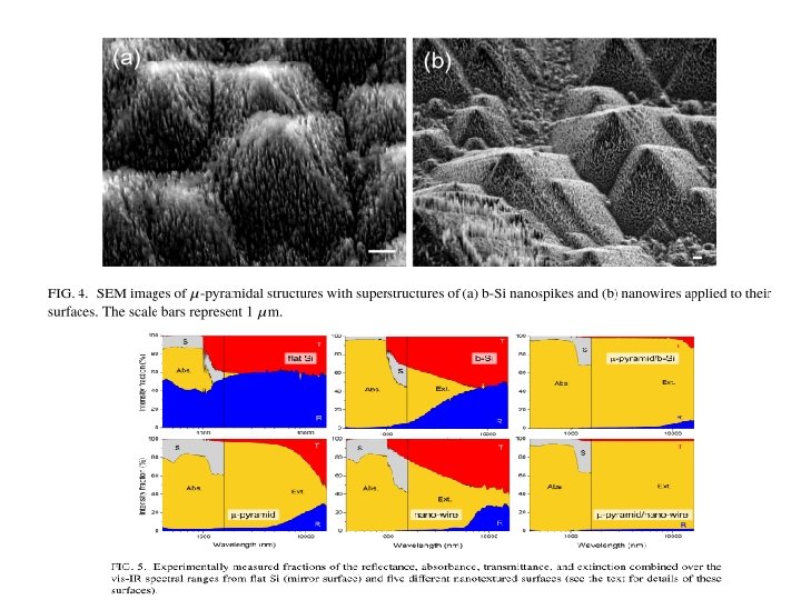
Hierarchical structures Example: Formation of antireflective black silicon From: Y. Nishijima at al. , Antireflective surfaces: Cascading nano/microstructuring, APL PHOTONICS 1, 076104 (2016).
- Slides: 23