TOPIC 1 ALTERNATING CURRENT THEORY RELATIONSHIP BETWEEN CURRENT

TOPIC 1: ALTERNATING CURRENT THEORY • RELATIONSHIP BETWEEN CURRENT AND VOLTAGE IN AN RC SERIES CIRCUIT: • In a purely resistive AC circuit, the current (IR) and the applied voltage (VR) are in phase. • In a purely capacitive AC circuit, the current (IC) leads the supply voltage (VC) by 90 degrees. • When there is a combination of resistance and capacitive reactance in an AC series circuit, the current (I) leads the supply voltage (V) by an angle between 0 and 90 degrees depending on the values of resistance and capacitive reactance.

FREQUENCY SELECTIVITY CHARACTERISTIC OF AN RC/RL/RLC SERIES CIRCUIT. • FREQUENCY SELECTIVITY: IS THE ABILITY OF A CIRCUIT TO SELECT A SPECIFIC FREQUENCY AND REJECT ALL OTHER FREQUENCIES. THE TWO TYPES OF FREQUENCY SELECTIVITY CHARACTERISTICS OF AN RC SERIES CIRCUIT ARE THE LOW-PASS FILTER AND THE HIGHPASS FLITER.

LOW-PASS FILTER AND HIGH-PASS FILTER • NB: CAPACITOR ALLOWS ONLY HIGH FREQUENCIES TO PASS. • AN INDUCTOR ALLOWS ONLY LOW FREQUENCIES TO PASS. • IDENTIFICATION OF LOW-PASS AND HIGH-PASS RC/RL CIRCUITS. • - WHAT REACHES THE OUTPUT • - WHAT IS IN THE SOURCE. • THE SOURCE MAY HAVE HIGH FREQUENCIES AND THE OUTPUT LOW FREQUENCIES, AND VICE VERSA. • THE FILTER IS IDENTIFIED ACCORDING TO WHAT THE OUTPUT FREQUENCY WILL BE.

LOW-PASS FILTER AND HIGH-PASS FILTER CIRCUITS • • • REFER TO: FIG. 2. 11 FOR LOW-PASS FILTER RL. FIG. 2. 12 FOR HIGH-PASS FILTER RL. FIG. 1. 15 & 1. 16 LOW-PASS FILTER RC. FIG. 1. 17 & 1. 18 HIGH-PASS FILTER RC.

LOW PASS FILTER RC

LOW PASS FILTER RL

High pass filter RC Circuit

HIGH PASS FILTER RL CIRCUIT
 is the frequency at which")
CUT-OFF FREQUENCY AND BANDWIDTH • THE CUT-OFF FREQUENCY (fc) is the frequency at which the capacitive / inductive reactance equals the resistance in a low –pass or highpass filter. • R = 1 / 2πfc. C • fc = 1/2πRC for RC Circuits. • fc = R / 2πL for RL Circuits. • At fc, the output voltage of RC / RL circuit is 70, 7 % or 1/√ 2 of its maximum value.

BANDWIDTH • BW – is the range of frequencies that pass from the input to the output of a circuit. • REFER TO FIG 1. 19 ON HOW TO FIND A BANDWIDTH USING THE VALUE 70. 7%

CUT-OFF FREQUENCY AND BANDWIDTH

EFFECTS OF FAULTY COMPONENTS ON RC SERIES CIRCUITS • OPEN RESISTOR: AN OPEN RESISTOR RESULTS IN NO CURRENT FLOW. THEREFORE, THE VOLTAGE ACROSS THE CAPACITOR IS 0 V AND THE TOTAL INPUT VOLTAGE WILL APPEAR ACROSS THE OPEN RESISTOR. • OPEN CAPACITOR: AN OPEN CAPACITOR RESUSLTS IN NO CURRENT FLOW. THEREFORE, THE VOLTAGE ACROSS THE RESISTOR IS 0 V AND THE TOTAL INPUT VOLTAGE WILL APPEAR ACROSS THE OPEN CAPACITOR. • SHORTED CAPACITOR: A SHORTED CAPACITOR RESULTS IN NO CURRENT FLOW. THEREFORE, THE VOLTAGE ACROSS THE CAPACITOR IS 0 V AND THE TOTAL INPUT VOLTAGE WILL APPEAR ACROSS THE RESISTOR. • LEAKY CAPACITOR: A LEAKY CAPACITOR WILL AFFECT THE RESPONSE OF THE CIRCUIT.

RC PARALLEL CIRCUIT • OPEN RESISTOR: An open resistor results in no current flow through the resistor, but the supply current will flow through the capacitor. Total input voltage will appear across the open resistor and capacitor as they are in parallel. • OPEN CAPACITOR: An open capacitor results in no current flow through the capacitor, but the supply current will flow through the resistor. The total input voltage will appear across the open capacitor and resistor as they are connected in parallel. • SHORTED CAPACITOR: A shorted capacitor will cause current to flow through the capacitor and can cause circuit damage. • LEAKY CAPACITOR: A leaky capacitor will affect the response of the circuit.

RL SERIES • OPEN RESISTOR: An open resistor results in no current flow. Therefore, voltage across the inductor is 0 V and the total input voltage appears across the open resistor. • OPEN INDUCTOR: An open inductor results in no current flow. Therefore, voltage appears across the resistor is 0 V and the total input voltage appears across the open inductor. • SHORTED WINDING ON INDUCTOR: A shorted winding results in less inductance in the inductor and has a negative effect on the performance of the circuit.

SERIES RESONANCE • RESONANCE FREQUENCY • Refer fig 3. 7 graph of reactance against frequency. • When the frequency is low, Xc is high whereas XL is low and the circuit is mainly capacitive. • When the frequency is increased, XL is high whereas Xc is low and the circuit is mainly inductive. • As the frequency is increased, Xc decreases and XL increases until a value is reached where XL = Xc and the two reactances cancel each other. The circuit is now said to be in resonance. This makes the circuit purely resistive where Z = R.

REACTANCE AGAINST FREQUENCY

RESONANCE CURCVE • THE RESONANCE CURVES FOR A TYPICAL RLC SERIES CIRCUIT ARE AS FOLLOWS: • AT RESONANCE, CURRENT (I) IS AT MAXIMUM AS SHOWN IN FIG. 3. 8. • AT RESONANCE, IMPENDANCE (Z) IS AT MINIMUM AS SHOWN IN FIG. 3. 9. • ALSO NOTE THAT THE SMALLER THE RESISTANCE IS , THE GREATER THE CURRENT IS. THE GREATER THE RESISTANCE IS, THE LESS THE CURRENT IS.

CURRENT AGAINST FREQUENCY

IMPENDANCE AGAINST FREQUENCY

CALCULATION OF SERIES RESONANCE FREQUENCY • SINCE AT RESONANCE XL = Xc • Therefore fr = 1 / (2π√LC) • EXAMPLE 3. 2

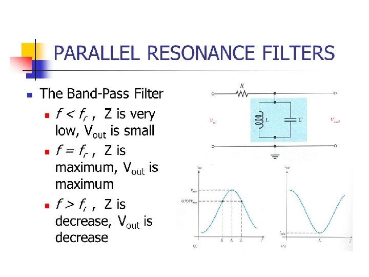
SERIES RESONANT FILTERS • BAND PASS FILTER • A particular band of frequencies sometimes needs to be filtered from a wider range of frequencies. By combining the properties of a low-pass and a high-pass filter, a band-pass filter is achieved. Refer to fig 3. 11.

BAND-PASS FILTER BLOCK DIAGRAM

Circuit of band pass filter

REFER FIG. 3. 12 • A series band-pass filter allows signals at the resonance frequency and at frequencies within a certain bandwidth to pass from the input to output as follows: • As the frequency increases, the impedance drops, therefore allowing more current to flow. As a result, more voltage develops across the resistor.

REFER TO FIG. 3. 13 • At the resonance frequency, the impedance is very low and is equal to the winding resistance of the coil. Maximum current occurs and the output voltage is also at its maximum. • Above the resonance frequency, the impedance increases. This results in less current flow which causes the output voltage to drop.

BANDWIDTH OF THE BAND-PASS FILTER

FORMULA FOR BANDWIDTH OF BANDPASS FILTER • BW = f 2 – f 1

Half-power points or frequencies • The upper and lower cut-off frequencies are sometimes called the half-power points or frequencies. This term is derived from the fact that the true power from the source at these frequencies is half the power delivered at the resonance frequency.
 of a resonant circuit • Calculating of the quality factor (Q)")
Quality factor (Q) of a resonant circuit • Calculating of the quality factor (Q) • The quality factor (Q) of a resonant circuit is the ratio of the reactive power in the inductor the true power in the winding resistance of the coil and other resistance in series with the coil. In other words, it is a ratio of the power L to the power in R. • Therefore: • Q = XL / R • = 2πf. L / R

Effect of Q on bandwidth

CONTN… • The bandwidth for a resonant circuit in terms of Q is: • BW = fr / Q • CALCULATIONS OF QUALITY FACTOR, RESONANCE FREQUENCY AND BANDWIDTH

PARALLEL RESONANCE • RESONANCE FREQUENCY • Similar to series resonance, when XL = Xc resonance occurs. The frequency at which resonance occurs is called resonance frequency. • When XL = Xc, Ic and IL are equal in magnitude but 180 degrees out of phase with each other. Refer fig 3. 22. Therefore, the total current (IT) is 0. • Since the total current is 0, the impedance of the parallel branch is infinitely large. • The phase angle is 0 degrees as the impedance is purely resistive at resonance frequency.

Resonance curve Current against frequency

Impedance against frequency Resonance curve

Calculation of parallel resonance frequency • The parallel resonance frequency is calculated as follows: • fr = 1/(2π√LC) • EXAMPLE 3. 6

Parallel resonant filters • Band pass filter, refer fig. 3. 26 • At low frequency, the impedance of the circuit is very low and therefore only small amount of voltage is dropped across it. • When the frequency increases, the impedance of the circuit increases. This causes the output voltage to increase. • At the resonance frequency, the impedance and output voltage are at their maximum. • Above the resonance frequency, the impedance begins to decrease. This causes the output voltage to decrease.

Effect of Q on bandwidth • A low Q value due to a high resistance in series with the inductor produces a flatter response curve for a parallel resonant circuit with the wider bandwidth. A high Q value is due to a low resistance in series with the inductor. This produces a higher peak and narrower bandwidth.

Calculations of parallel resonant filters • Example 3. 7 • Example 3. 8

APPLICATIONS FOR RESONANT CIRCUITS • • TUNED AMPLIFIERS RADIO ANTENNA COUPLINGS RADIO RECEIVERS LOAD IMPEDANCE

TOPIC 2 FUNDAMENTALS OF ELECTRONICS • • • MODULE 4 - OUTCOMES AT THE END OF THIS MODULE, YOU SHOULD BE ABLE TO: COMPARE AN AMPLIFIER TO AN OSCILLATOR. EXPLAIN THE DIFFERENCE BETWEEN DAMPED AND UNDAMPED OSCILLATIONS. EXPLAIN HOW OSCILLATIONS ARE PRODUCED IN AN LC CIRCUIT AND CALCULATE OSCILLATION FREQUENCY.

MODULE OUTCOMES CONTN… • LIST FACTORS THAT AFFECT OSCILLATION FREQUENCY. • DESCRIBE THE OPERATION OF OSCILLATOR CIRCUITS AND CALCULATE OSCILLATION FREQUENCY. Range: Phase shifts, Colpitts, Hartley, and Wien bridge oscillator. • SKETCH AND DESCRIBE THE OPERATION OF A CRYSTAL OSCILLATOR CIRCUIT.

UNIT 4. 1: BASIC PRINCIPLES OF OSCILLATORS AMPLIFIERS VERSUS OSCILLATORS

NON-SINUSOIDAL OSCILLATORS • MULTIVIBRATORS. • Oscillators, timers and flip-flops are examples of multivibrators.
 amp is an electronic device that")
AMPLIFIER • An amplifier, electronic amplifier or (informally) amp is an electronic device that can increase the power of a signal. It does this by taking energy from a power supply and controlling the output to match the input signal shape but with a larger amplitude.

OP-AMP

OSCILLATOR • An electronic oscillator is an electronic circuit that produces a periodic, oscillating electronic signal, often a sine wave or a square wave. Oscillators convert direct current (DC) from a power supply to an alternating current signal. They are widely used in many electronic devices.

OSCILLATOR STRUCTURE

POSITIVE FEEDBACK • The return of part of an output signal to the input, which is in phase with it, so that the amplifier gain is increased and often the output is distorted.

DAMPED OSCILLATIONS

UNDAMPED OSCILLATIONS

OSCILLATION IN AN LC CIRCUIT

PHASE SHIFT OSCILLATOR

COLPITS OSCILLATOR

HARTLEYOSCILLATOR

Wien bridge oscillator

CRYSTAL OSCILLATOR

MODULE 5 – NON-SINUSOIDAL OSCILLATORS • A NON-SINUSOIDAL OSCILLATOR PRODUCES A NON-SINUSOIDAL OUTPUT SUCH AS A SQUARE, SAWTOOTH, OR TRIANGULAR WAVE. IT CONTAINS AN ENERGY STORING ELEMENT, FOR EXAMPLE A CAPACITOR, AND A NONLINEAR SWITCHING CIRCUIT, SUCH AS A LATCH, THAT PERIODICALLY CHARGES AND DISCHARGES THE ENERGY STORED IN THE STORAGE ELEMENT. THIS CAUSES CHANGES IN THE OUTPUT WAVEFORM.

MODULE OUTCOMES • EXPLAIN THE DIFFERENCE BETWEEN SINUSOIDAL AND NON-SINUSOIDAL OSCILLATORS. • DESCRIBE THE OPERATION OF TRANSISTOR MULTIVIBRATORS. Range: Astable, bistable and monostable multivibrators. • LIST THE APPLICATIONS OF MULTIVIBRATORS • EXPLAIN THE CIRCUIT OPERATION OF A 555 TIMER IN ASTABLE AND MONOSTABLE MODE.

UNIT 5. 1: MULTIVIBRATORS • A SINUSOIDAL OSCILLATOR PRODUCES A SINE WAVE OUTPUT SIGNAL WITH CONSTANT AMPLITUDE AND WITH NO CHANGE IN FREQUENCY. OSCILLATORS WHICH GENERATE WAVEFORMS OTHER THAN SINE WAVES, FOR EXAMPLE SQUARE, TRIANGULAR, RECTANGULAR AND SAWTOOTH WAVEFORMS, ARE REFERRED TO AS NONSINUSOIDAL OSCILLATORS.

TRANSISTOR MULTIVIBRATORS TYPES OF MULTIVIBRATORS • A MULTIVIBRATOR IS AN ELECTRONIC CIRCUIT USED TO IMPLEMENT A VARIETY OF SIMPLE TWO -STATE SYSTEMS. OSCILLATORS, TIMERS AND FLIP -FLOPS ARE EXAMPLES OF MULTIVIBRATORS. A MULTIVIBRATOR IS CHARACTERISED BY TWO AMPLIFYING DEVICES CROSS-COUPLED BY RESISTORS OR CAPACITORS. THERE ARE THREE BASIC TYPES OF MULTIVIBRATOR CIRCUITS DEPENDING ON THE TYPE OF COUPLING METHOD USED: ASTABLE, BISTABLE AND MONOSTABLE.

ASTABLE MULTIVIBRATORS • WITH AN ASTABLE MULTIVIBRATOR, THE CIRCUIT IS NOT STABLE IN EITHER STATE AS IT CONTINUALLY SWITCHES FROM ONE STATE TO THE OTHER. ASTABLE MULTIVIBRATORS ARE ALSO KNOWN AS FREE-RUNNING MULTIVIBRATORS AS THEY DO NOT REQUIRE ANY INPUTS TO PROVIDE OSCILLATION. THEY ARE COMMONLY USED TO GENERATE SQUARE WAVEFORMS.

ASTABLE MULTIVIBRATOR CIRCUIT DIAGRAM

COMPONENTS • An astable multivibrator circuit diagram with 2 LEDs • This is a classic oscillator circuit. • The Light-Emitting Diode (LED) on the left side is lit when the transistor on the left side (Q 1) is ON. The LED on the right side is lit when the transistor on the right side (Q 2) is ON. • Resistors R 1 and R 4 are only there to set the current through the LEDs. • Which means the remaining six components make up the oscillator: Q 1, Q 2, C 1, C 2, R 2, and R 3.

OPERATION

Operation detailed explanation • The astable multivibrator circuit is a classic circuit for flashing two LEDs. It doesn’t have to flash two LEDs though. It can blink just one LED. Or it can create a tone to play on a speaker. • First, let me show you the circuit in action: • Want to know theory behind how the circuit works? • There have been many attempts to explain this circuit. Most have failed to explain it to other than those already beyond the beginner level.

Understanding the Astable Multivibrator • The voltage on the left side of C 2 controls transistor Q 1. • The voltage on the right side of C 1 controls transistor Q 2. • When transistor Q 1 turns ON, it changes the voltage of C 1 so that Q 2 turns off. • After a short while, the voltage of C 1 rises back up and turns on the transistor Q 2. • When transistor Q 2 turns on, it changes the voltage of C 2 so that Q 1 turns off.

OPERATION CONTN… • If you want to really understand how the astable multivibrator circuit works, you have to look more detailed at how the voltages over the two capacitors behave. • What do you need to know? • You need to know how transistors work. • And it is important that you have a good understanding of how voltages behave in a circuit, and how current flows.

OPERATION CONTN. . • 1. Voltage is always measured between two points. • When we talk about the voltage at one specific point, it means the voltage measured from that point to the minus of the battery. (That’s why we call the minus of the battery 0 V) • 2. Think about the transistor as a switch. • It needs 0. 7 V on the middle pin (base) to turn ON. When it is ON, its top pin (collector) connects down to its bottom pin (emitter) so that current can flow through it. • This also means that the top pin has the same voltage as the bottom pin when the transistor is on. When the transistor is OFF, there are no connections between the top pin and the bottom pin, so no current can flow.

When LED 1 is on • Let’s start by looking at the circuit when the LED L 1 is lit and the other LED is off.

CONTN… • The voltage on the right of capacitor C 2 quickly reaches 7 -8 V when the LED on the left is lit. • L 1 is only lit when transistor Q 1 is ON. • We know from how transistors work that Q 1 is only turned ON if it has 0. 7 V on its base. Since the left side of C 2 connects to the base of Q 1, that means it’s at 0. 7 V. • The right side of the capacitor C 2 connects to 9 V through R 4 and L 2, so it is charging and the voltage is rising. • A capacitor charges exponentially, which means the voltage rises quickly in the beginning, then slows down more and more. The voltage reaches 7 -8 V quickly, but from there the voltage rises slowly.

VOLTAGES AROUND Q 2

CONTN… • The voltage on the right of C 1 is somewhere below 0. 7 V, but increasing, when the left LED is lit • Since the transistor Q 2 is off, its base must be lower than 0. 7 V. • The right side of C 1 connects to the base of Q 2, so that means this is also lower than 0. 7 V. • But the right side of C 1 is also connected to 9 V through the resistor R 2, which means it is being charged. • That means the voltage is below 0. 7 V but rising.

The Turning Point • So, the voltage on the right side of C 1 is rising. • And when it reaches 0. 7 V, the action starts! • When the right side of C 1 reaches 0. 7 V, that means the base of transistor Q 2 gets 0. 7 V on its base and turns on. • …which means the LED on the right also turns on. • But when Q 2 turns on, something interesting happens with the voltages we had over the capacitor C 2…

Getting a negative voltage • We had that C 2 had 0. 7 V on its left side and 8 V on its right side. • Or to say it in another way, the left side was 7. 3 V lower than the right side. • But now that Q 2 turns on, the voltage on the right side of C 2 is suddenly pulled down to 0 V through the transistor. • The internal charge of the capacitor does not change though, so the left side keeps being 7. 3 V lower than the right side. • But now that the right side is 0 V, that means the left side becomes 7. 3 V below 0! • Yes, that’s -7. 3 V.

Transistor Q 1 gets minus on its base • With -7. 3 V on the left side of C 2, the base of transistor Q 1 also gets -7. 3 V on its base, which turns it off.

END OF EXPLANATION • When transistor Q 2 turns on, the transistor and LED on the left turn off. • So now, the left LED and transistor have turned off. And the right LED and transistor have turned on. • The left side of C 2 starts at -7. 3 V and is charged through resistor R 3 and therefore rising. Since it connects to the base of transistor Q 1, when it reaches 0. 7 V, Q 1 turns on again. • And so it continues. • The two transistors keep alternating between on and off, which makes the two LEDs alternate between on and off.

MONOSTABLE MULTIVIBRATOR CIRCUIT DIAGRAM

BISTABLE MULTIVIBRATOR

555 TIMER BLOCK DIAGRAM

555 timer IC

555 TIMER PIN CONFIGURATION • Pin 1 • It is the ground pin directly connected to the negative rail. It should not be connected using a resistor, because all the semiconductors inside the IC will heat up due to stray voltage accumulating in it. • Pin 2 • It is the Trigger pin to activate the IC’s timing cycle. It is generally low signal pin and the timer is triggered when voltage on this pin is below one third of the supply voltage. The trigger pin is connected to the Inverting input of the comparator inside the IC and accepts negative signals. The current required for triggering is 0. 5 u. A for a period of 0. 1 u. S. The triggering voltage maybe 1. 67 V if the supply voltage is 5 V and 5 V if the supply voltage is 15 V. The triggering circuit inside the IC is too sensitive so that the IC will show false triggering due to noise in the surroundings. It requires a pull up connection to avoid false triggering.

• Pin 3 • It is the output pin. When the IC triggers via pin 2, the output pin goes high depending on the duration of the timing cycle. It can either sink or source current which is at maximum 200 m. A. For logic zero output, it is sinking current with voltage slightly greater than zero. For logic high output, it is sourcing current with the output voltage slightly lesser than Vcc. • Pin 4 • It is the reset pin. It should be connected to the positive rail to work the IC properly. When this pin is grounded, the IC will stop working. The reset voltage required for this pin should be 0. 7 volts at a current of 0. 1 m. A.

• Pin 5 • Control pin – The 2/3 supply voltage point on the terminal voltage divider is brought to the control pin. It requires to be connected to an external DC signal to modify the timing cycle. When not in use, it should be connected to the ground through a 0. 01 u. F capacitor; otherwise the IC will show erratic responses • Pin 6 • It is the Threshold pin. The timing cycle is completed when voltage on this pin is equal to or greater than twothird of Vcc. It is connected to the non inverting input of the upper comparator so that it accepts the positive going pulse to complete the timing cycle. Typical threshold current is 0. 1 m. A as in the case of Reset pin. The time width of this pulse should be equal or greater

• Pin 7 • Discharge pin. It provides a discharge path for the timing capacitor through the collector of the NPN transistor, to which it is connected. The maximum allowable discharging current should be less than 50 m. A otherwise the transistor may damage. It can be also used as an open collector output. • Pin 8 • It is positive rail connected pin which is connected to positive terminal of the power supply. It is also known as Vcc. IC 555 works in a wide range of voltage from 5 V to 18 V DC where as the CMOS version 7555 works with 3 Volts.

TIMER IN ASTABLE MODE

555 TIMER IN MONOSTABLE MODE

UNIT 7. 3: TRANSISTOR AND FEEDBACK AMPLIFIERS • THE PURPOSE OF THE FINAL STAGE OF ANY AMPLIFICATION SYSTEM IS TO ENSURE A LOW OUTPUT RESISTANCE SO THAT THE OUTPUT SIGNAL MAY BE DELIVERED TO A LOW-RESISTANCE LOAD WITHOUT LOSS OF GAIN. OTHER REQUIREMENTS OF AN AMPLIFIER ARE THAT SIGNAL DISTORTION MUST BE KEPT TO A MINIMUM AND IT MUST DELIVER THE REQUIRED POWER TO THE LOAD EFFICIENTLY. • AMPLIFIERS ARE CLASSIFIED ACCORDING TO THE CHARACTERISTICS OF THE COLLECTOR (OUTPUT) CURRENT WAVEFORM WITH AN APPLIED INPUT SIGNAL. THERE ARE THREE MAIN CLASSES OF AMPLIFIERS: CLASS A, CLASS B AND CLASS C.

CLASS A AMPLIFIERS • WAVEFORM OF A CLASS A AMPLIFIER. • In a class A amplifier the transistor bias and the amplitude of the input signal are such that the output current flows for the complete cycle of the input signal. Refer fig 7. 28 textbooks. • It is a common emitter amplifier, the Q point is set at the centre of the load line. Refer to fig 7. 29.

CHARACTERISTICS OF A CLASS A AMPLIFIER • THE OUTPUT CURRENT FLOWS DURING THE ENTIRE CYCLE OF AC INPUT SIGNAL. • THE OPERATION OF THE AMPLIFIER IS RESTRICTED TO THE SMALLER CENTRAL REGION OF LOAD LINE SO THAT IT CAN OPERATE IN THE LINEAR REGION OF THE LOAD LINE. • SINCE THE TRANSISTOR OPERATES OVER THE LINEAR REGION OF THE LOAD LINE, THE OUTPUT WAVEFORM IS SIMILAR TO THE INPUT WAVEFORM. • IT HAS AN EFFICIENCY OF BETWEEN 25 AND 50%.

CLASS B AMPLIFIERS • In a class B amplifier the transistor bias and the amplitude of the input signal are such that the output current flows for only half the cycle or 180 degrees of the input signal. Refer to fig 7. 30 textbooks. • The Q point is set at cut-off or at the lower end of the load line. Refer to fig 7. 31. • With no input signal, the transistor is biased at cut-off. At this point, there is no current flow through the transistor and hence no power is dissipated by the transistor. However, when the signal is applied, the transistor handles an average current which increases it for large input signals.

CHARACTERISTICS OF A CLASS B AMPLIFIER • THE OUTPUT CURRENT FLOWS ONLY FOR ONE HALF CYCLE OR 180 DEGREES OF THE INPUT SIGNAL. • THE TRANSISTOR DISSIPATES NO POWER WITH ZERO INPUT SIGNAL. HOWEVER, IT INCREASES WITH THE AMPLITUDE OF THE INPUT SIGNAL. • THE AVERAGE CURRENT DRAWN BY THE CIRCUIT IS SMALLER THAT OF A CLASS A AMPLIFIER. • IT HAS AN EFFICIENCY OF 78%.

CLASS CAMPLIFIERS • In a class C amplifier the transistor bias and the amplitude of the input signal are such that output current flows for less than half the cycle or less than 180 degrees of the input signal. Refer fig 7. 32 textbooks. The Q point is beyond the cut-off region and current flows for less than half the cycle of the input signal. These amplifiers are used in oscillator circuits. • Refer to fig 7. 33 in your textbooks.

CHARACTERISTICS OF A CLASS C AMPLIFIER • THE OUTPUT CURRENT FLOWS ONLY DURING PART OF THE POSITIVE OR NEGATIVE HALF CYCLE OF THE INPUT SIGNAL. THIS CONDITION IS ACHIEVED BY BIASING THE TRANSISTOR BELOW CUT-OFF. • THE OUTPUT SIGNAL DOES NOT RESEMBLE THE INPUT SIGNAL AS IT CONSISTS OF PULSES. • A CLASS C AMPLIFIER IS EFFICIENT – ITS EFFICIENCY MAY APPROACH 100%.

CLASS B PUSH-PULL AMPLIFIER • A CLASS B AMPLIFIER FLOWS FOR ONLY HALF A CYCLE OR 180 degrees OF THE INPUT SIGNAL. REFER FIG 7. 34. FOR THE TRANSISTOR TO CONDUCT IN THE OTHER HALF CYCLE, A SECOND CLASS B AMPLIFIER MUST BE ADDED. THE COMBINATION IS REFERRED TO AS A PUSH-PULL OPERATION. THE TWO WAYS TO ACHIEVE A PUSH-PULL OPERATION ARE BY USING A TRANSFORMER COUPLING OF COMPLEMENTARY SYMMETRY TRANSISTORS.

TRANSFORMER COUPLING • FIG. 7. 35 SHOWS A TRANSFORMER COUPLING CLASS B PUSH-PULL AMPLIFIER. THE CENTRE TAPPED INPUT TRANSFORMER PRODUCES THE OUT-OF-PHASE INPUT SIGNAL FOR THE TWO NPN TRANSISTORS. Q 1 CONDUCTS IN THE POSITIVE CYCLE WHILE Q 2 CONDUCTORS IN THE NEGATIVE HALF CYCLE. THE OUTPUT TRANSFOMER COMBINES THE TWO OTUPUTS OF Q 1 AND Q 2. TRANSISTORS Q 1 AND Q 2 ARE BIASED AT CUT-OFF.

COMPLEMENTARY SYMMETRY TRANSISTORS • A CLASS B AMPLIFIER WITH COMPLEMENTARY SYMMETRY TRANSISTORS CONSISTS OF TWO EMITTER-FOLLOWERS AND BOTH POSITIVE AND NEGATIVE SUPPLIES. THIS IS A COMPLEMENTARY AMPLIFIER AS Q 1 IS NPN WHILE Q 2 IS PNP TRANSISTOR. Q 1 CONDUCTS IN POSITIVE HALF CYCLE, SEE FIG 7. 36. Q 2 CONDUCTS IN THE NEGATIVE CYCLE AS SHOWN IN FIG 7. 37.

ADVANTAGES OF CLASS B PUSH-PULL AMPLIFIER • THE CIRCUIT EFFICIENCY OF A CLASS B PUSHPULL AMPLIFIER IS CLOSE TO 80% WHICH IS HIGHER THAN THAT OF A CLASS A AMPLIFIER. • IT ELIMINATES HARMONICS IN THE AC OUTPUT SIGNAL. • THERE IS NO DC COMPONENT IN THE OUTPUT SIGNAL.

DISADVANTAGES OF A CLASS B PUSHPULL AMPLIFIER • A CLASS B PUSH-PULL AMPLIFIER REQUIRES PHASE-SPLITTING COMPONENT THAT MAKES IT MORE COMPLEX AND MORE EXPENSIVE. • THE USE OF CENTRE-TAPPED TRANSFORMERS ADDS WEIGHT AND RESTRICTS PERFORMANCE. • DISTORTION CAN BE INTRODUCED IF THE TWO PARTS OF THE AMPLIFIER DO NOT HAVE IDENTICAL CHARACTERISTICS.

APPLICATIONS OF A CLASS B PUSHPULL AMPLIFIER • CLASS B PUSH-PULL AMPLIFIERS ARE WIDELY USED IN MANY AMPLIFIER OUTPUT STAGES.

FEEDBACK AMPLIFIERS • AN AMPLIFIER AMPLIFIES SIGNALS. A DISTURBANCE AT THE INPUT APPEARS IN AMPLIFIED FORM AT THE OUTPUT. FOR EXAMPLE, AMPLIFIERS CAN INTRODUCE HUM DUE TO TEMPERATURE CHANGE OR STRAY MAGNETIC FIELDS. THE NOISE AT THE OUTPUT OF AN AMPLIFIER IS UNWANTED AND MUST BE KEPT TO A MINIMUM. THIS PROBLEM CAN BE OVERCOME BY USING FEEDBACK.

FEEDBACK • FEEDBACK IS THE PROCESS OF RETURNING SOME ENERGY FROM THE OUTPUT TO THE INPUT. REFER TO FIG 7. 38. • THERE ARE TWO BASIC TYPES OF FEEDBACK USED IN AMPLIFIERS DEPENDING ON WHETHER THE FEEDBACK INCREASES OR DECREASES THE SIGNAL. POSITIVE FEEDBACK AND NEGATIVE FEEDBACK
 IS APPLIED IN SUCH")
POSITIVE FEEDBACK • IF THE FEEDBACK SIGNAL (VOLTAGE OR CURRENT) IS APPLIED IN SUCH A WAY THAT IT IS IN PHASE WITH THE INPUT SIGNAL AND THUS INCREASES IT, THEN IT IS CALLED POSITIVE FEEDBACK. WHILE POSITIVE FEEDBACK INCREASES THE GAIN OF THE AMPLIFIER
 is applied in such")
NEGATIVE FEEDBACK • If the feedback signal (voltage or current) is applied in such a way that it is out of phase with the input signal and thus decreases it, then it is called negative feedback. While negative feedback reduces the gain of the amplifier, it improves amplifier performance in many other respects. Negative feedback is frequently used in small-signal as well as in large –signal amplifier circuits.

Advantages of negative feedback • Improves stability • Increases the operating bandwidth • Reduces distortion and noise.

Types of feedback signals • Feedback signals can be divided into two types: Series and Shunt (parallel). • Series feedback connections tend to increase the input resistance while shunt feedback connections tend to decrease input resistance. Voltage feedback tends to decrease the output resistance while the current feedback tends to increase the output resistance.

TYPES OF CONNECTIONS • There are four ways of connecting negative feedback signals. Both voltage and current can be fed back to the input either in series or in parallel as follows: • Voltage series feedback – refer fig 7. 39 • Current series feedback – refer fig 7. 40 • Voltage-shunt feedback – refer fig 7. 41 • Current-shunt feedback – refer fig 7. 42

APPLICATIONS OF FEEDBACK CONNECTIONS • NEGATIVE FEEDBACK IS WIDELY USED IN ELECTRONIC AMPLIFIERS SUCH AS AUDIO AND TV CIRCUITS BECAUSE OF ITS MANY ADVANTAGES. THE FOLLOWING BASIC TRANSISTOR AMPLIFIER CIRCUITS USE NEGATIVE FEEDBACK. • FIG 7. 43 TWO STAGE AMPLIFIER CIRCUIT • FIG 7. 44 COMMON EMITTER AMPLIFIER WITHOUT BYPASS CAPACITOR. • COMMON EMITTER AMPLIFIER WITH BYPASS CAPACITOR.

MODULE 8: SCRs AND TRIACS • SCR – is a semiconductor switching device that is widely used in electronics. It can handle currents of up to several thousand amperes and voltages up to more than 1 k. V. An SCR requires a control circuit which triggers it into conduction by means of a gate pulse. • If a positive voltage pulse is applied to the gate of the SCR, it will start to conduct like a normal diode. The conduction can only be stopped by removing the positive voltage from its anode.

Triac • A Triac is a three-electrode semiconductor device that will conduct in either direction when triggered by a positive or negative signal at the gate terminal. The name of the device is derived from triode and AC. A triode is a semiconductor rectifier that has three connections.
- Slides: 111