Timing Based Sparse Readout of Pixels in Deep
Timing Based Sparse Readout of Pixels in Deep Submicron CMOS Jean-François Genat LPNHE Paris In collaboration with LAL and LAPP Omegapix Journées VLSI IAO/CAO IPN Lyon, 5 -7 Juin 2012 26/10/2021 1
Motivations Reduce: - Pixel processing silicon area - Readout time - Power Journées VLSI IAO/CAO IPN Lyon, 5 -7 Juin 2012 26/10/2021 2
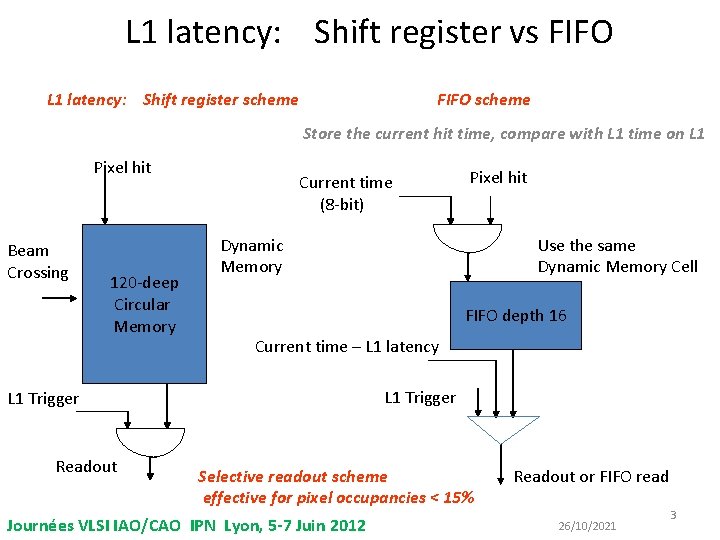
L 1 latency: Shift register vs FIFO L 1 latency: Shift register scheme FIFO scheme Store the current hit time, compare with L 1 time on L 1 Pixel hit Beam Crossing 120 -deep Circular Memory Current time (8 -bit) Dynamic Memory Use the same Dynamic Memory Cell FIFO depth 16 Current time – L 1 latency L 1 Trigger Readout Pixel hit Selective readout scheme effective for pixel occupancies < 15% Journées VLSI IAO/CAO IPN Lyon, 5 -7 Juin 2012 Readout or FIFO read 26/10/2021 3
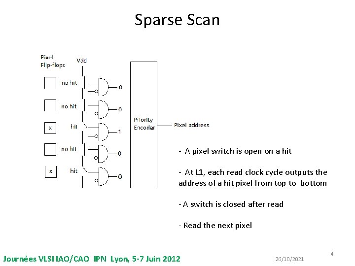
Sparse Scan - A pixel switch is open on a hit - At L 1, each read clock cycle outputs the address of a hit pixel from top to bottom - A switch is closed after read - Read the next pixel Journées VLSI IAO/CAO IPN Lyon, 5 -7 Juin 2012 26/10/2021 4
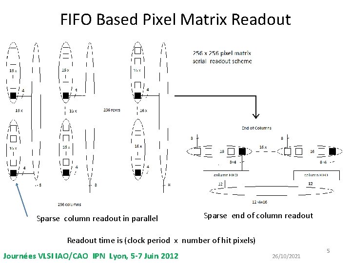
FIFO Based Pixel Matrix Readout Sparse column readout in parallel Sparse end of column readout Readout time is (clock period x number of hit pixels) Journées VLSI IAO/CAO IPN Lyon, 5 -7 Juin 2012 26/10/2021 5
FIFO Based Pixel Matrix Readout -Data stay for one L 1 latency in the FIFO at more -The FIFO outputs its oldest data - On L 1, if time match, data is output, otherwise, thrown away - FIFO contains time hit informations instead of mostly zeros - Requires arithmetic at the pixel level - FIFO size depends upon occupancy and affordable deadtime Journées VLSI IAO/CAO IPN Lyon, 5 -7 Juin 2012 26/10/2021 6

Inefficiency vs FIFO Depth Occupancy: Time used for pulse shaping over total time e. g. Deadtime: At 1 k. Hz rate at 500 ns shaping time: occupancy is 5 10 -4 Average channel blind time over total time for a given L 1 latency and FIFO depth (due to FIFO full occurence - 5% occupancy, - 3 ms L 1 latency and FIFO depth of 10 deadtime is less than 1/1000 Journées VLSI IAO/CAO IPN Lyon, 5 -7 Juin 2012 26/10/2021 7

Inefficiency vs FIFO depth Journées VLSI IAO/CAO IPN Lyon, 5 -7 Juin 2012 26/10/2021 8
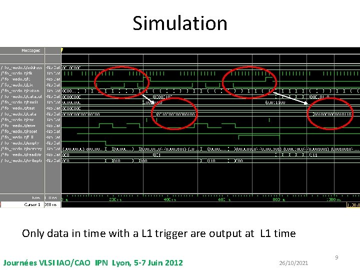
Simulation Only data in time with a L 1 trigger are output at L 1 time Journées VLSI IAO/CAO IPN Lyon, 5 -7 Juin 2012 26/10/2021 9
Status… - Synthesize using TSMC 65 nm CMOS digital library Design kit received this week… - Compare the full pixel hardware with present shift register implementation Journées VLSI IAO/CAO IPN Lyon, 5 -7 Juin 2012 26/10/2021 10
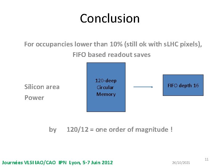
Conclusion For occupancies lower than 10% (still ok with s. LHC pixels), FIFO based readout saves Silicon area Power by 120 -deep Circular Memory FIFO depth 16 120/12 = one order of magnitude ! Journées VLSI IAO/CAO IPN Lyon, 5 -7 Juin 2012 26/10/2021 11
- Slides: 11