TIMERS The 555 Timer The 555 Timer is

- Slides: 36

TIMERS

The 555 Timer • The 555 Timer is one of the most popular and versatile integrated circuits ever produced! • It is 30 years old and still being used! • It is a combination of digital and analog circuits. • It is known as the “time machine” as it performs a wide variety of timing tasks. • 555 timer operate in several modes: 1. Monostable mode 2. Astable mode 3. Bistable mode 4. Buffer – Schmitt trigger

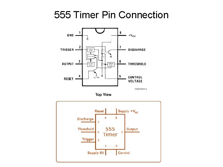
555 Timer Pin Connection

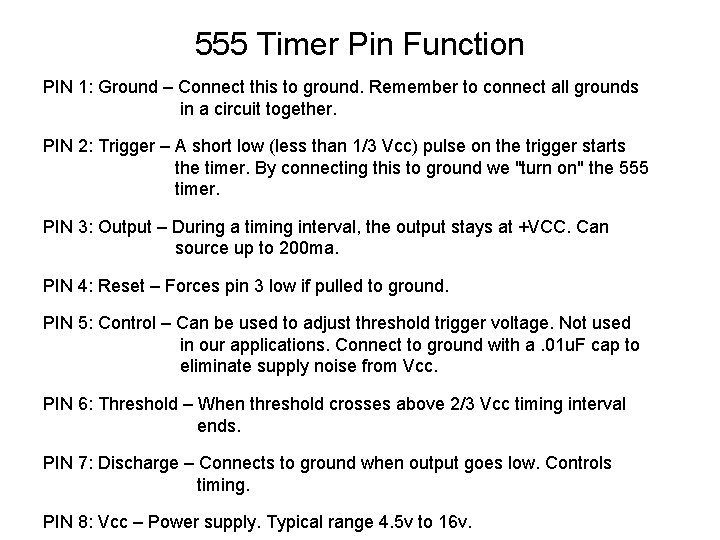
555 Timer Pin Function PIN 1: Ground – Connect this to ground. Remember to connect all grounds in a circuit together. PIN 2: Trigger – A short low (less than 1/3 Vcc) pulse on the trigger starts the timer. By connecting this to ground we "turn on" the 555 timer. PIN 3: Output – During a timing interval, the output stays at +VCC. Can source up to 200 ma. PIN 4: Reset – Forces pin 3 low if pulled to ground. PIN 5: Control – Can be used to adjust threshold trigger voltage. Not used in our applications. Connect to ground with a. 01 u. F cap to eliminate supply noise from Vcc. PIN 6: Threshold – When threshold crosses above 2/3 Vcc timing interval ends. PIN 7: Discharge – Connects to ground when output goes low. Controls timing. PIN 8: Vcc – Power supply. Typical range 4. 5 v to 16 v.

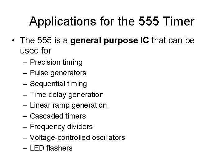
Applications for the 555 Timer • The 555 is a general purpose IC that can be used for – – – – – Precision timing Pulse generators Sequential timing Time delay generation Linear ramp generation. Cascaded timers Frequency dividers Voltage-controlled oscillators LED flashers

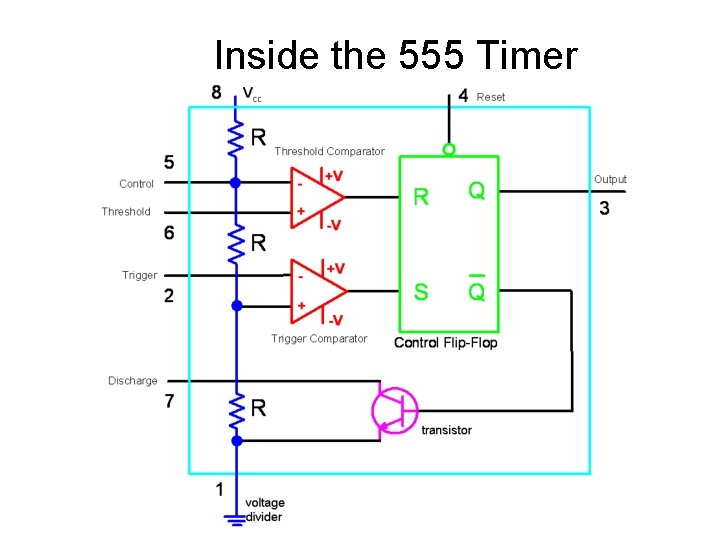
Inside the 555 Timer

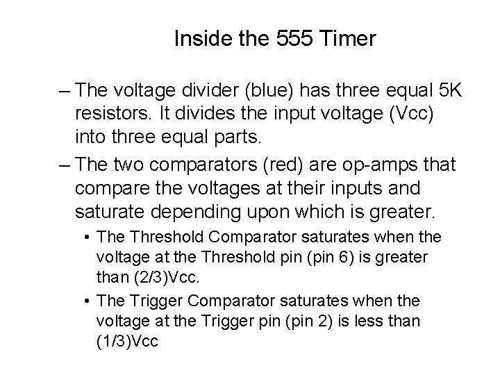
Inside the 555 Timer – The voltage divider (blue) has three equal 5 K resistors. It divides the input voltage (Vcc) into three equal parts. – The two comparators (red) are op-amps that compare the voltages at their inputs and saturate depending upon which is greater. • The Threshold Comparator saturates when the voltage at the Threshold pin (pin 6) is greater than (2/3)Vcc. • The Trigger Comparator saturates when the voltage at the Trigger pin (pin 2) is less than (1/3)Vcc

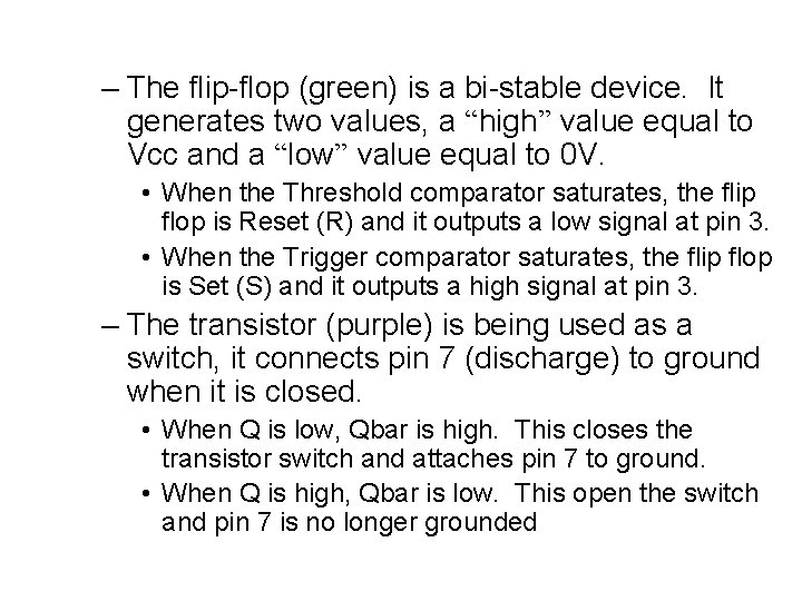
– The flip-flop (green) is a bi-stable device. It generates two values, a “high” value equal to Vcc and a “low” value equal to 0 V. • When the Threshold comparator saturates, the flip flop is Reset (R) and it outputs a low signal at pin 3. • When the Trigger comparator saturates, the flip flop is Set (S) and it outputs a high signal at pin 3. – The transistor (purple) is being used as a switch, it connects pin 7 (discharge) to ground when it is closed. • When Q is low, Qbar is high. This closes the transistor switch and attaches pin 7 to ground. • When Q is high, Qbar is low. This open the switch and pin 7 is no longer grounded

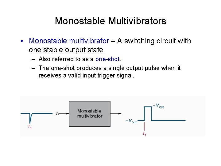
Monostable Multivibrators • Monostable multivibrator – A switching circuit with one stable output state. – Also referred to as a one-shot. – The one-shot produces a single output pulse when it receives a valid input trigger signal.

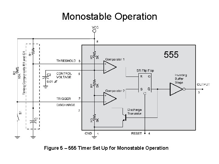
Monostable Operation Figure 5 – 555 Timer Set Up for Monostable Operation

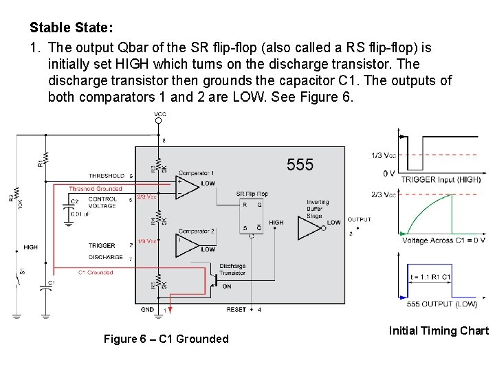
Stable State: 1. The output Qbar of the SR flip-flop (also called a RS flip-flop) is initially set HIGH which turns on the discharge transistor. The discharge transistor then grounds the capacitor C 1. The outputs of both comparators 1 and 2 are LOW. See Figure 6 – C 1 Grounded Initial Timing Chart

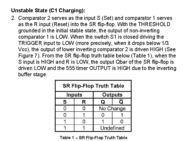
Unstable State (C 1 Charging): 2. Comparator 2 serves as the input S (Set) and comparator 1 serves as the R input (Reset) into the SR flip-flop. With the THRESHOLD grounded in the initial stable state, the output of non-inverting comparator 1 is LOW. When the switch S 1 is closed driving the TRIGGER input to LOW (more precisely, when it drops below 1/3 Vcc), the output of lower inverting comparator 2 is driven HIGH (See Figure 7). From the SR flip-flop truth table below (Table 1), when the S input is HIGH and R is LOW, the output Qbar of the SR flip-flop is driven LOW and the 555 timer OUTPUT is HIGH due to the inverting buffer stage. Table 1 – SR Flip-Flop Truth Table

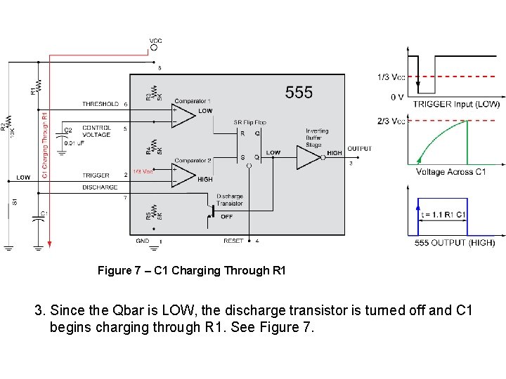
Figure 7 – C 1 Charging Through R 1 3. Since the Qbar is LOW, the discharge transistor is turned off and C 1 begins charging through R 1. See Figure 7.

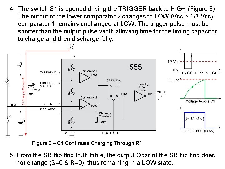
4. The switch S 1 is opened driving the TRIGGER back to HIGH (Figure 8). The output of the lower comparator 2 changes to LOW (Vcc > 1/3 Vcc); comparator 1 remains unchanged at LOW. The trigger pulse must be shorter than the output pulse width allowing time for the timing capacitor to charge and then discharge fully. Figure 8 – C 1 Continues Charging Through R 1 5. From the SR flip-flop truth table, the output Qbar of the SR flip-flop does not change (S=0 & R=0), thus remaining in a LOW state.

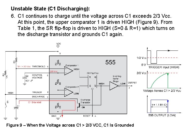
Unstable State (C 1 Discharging): 6. C 1 continues to charge until the voltage across C 1 exceeds 2/3 Vcc. At this point, the upper comparator 1 is driven HIGH (Figure 9). From Table 1, the SR flip-flop is driven to HIGH (S=0 & R=1) which turns on the discharge transistor and grounds C 1 again. Figure 9 – When the Voltage across C 1 > 2/3 VCC, C 1 Is Grounded

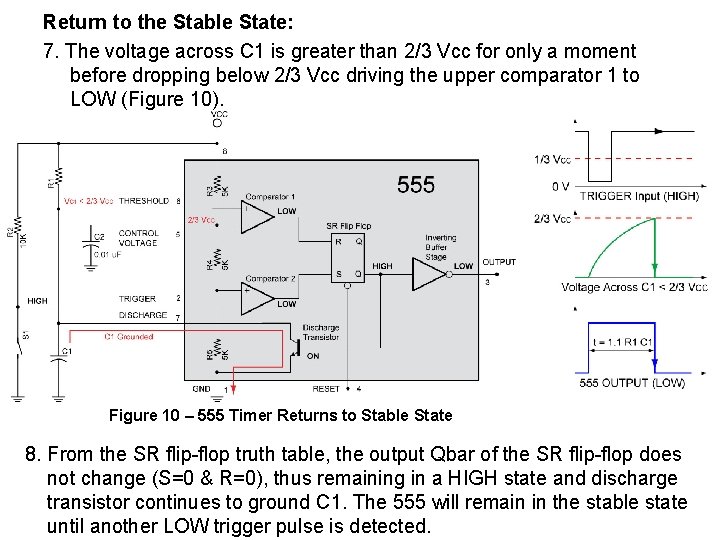
Return to the Stable State: 7. The voltage across C 1 is greater than 2/3 Vcc for only a moment before dropping below 2/3 Vcc driving the upper comparator 1 to LOW (Figure 10). Figure 10 – 555 Timer Returns to Stable State 8. From the SR flip-flop truth table, the output Qbar of the SR flip-flop does not change (S=0 & R=0), thus remaining in a HIGH state and discharge transistor continues to ground C 1. The 555 will remain in the stable state until another LOW trigger pulse is detected.

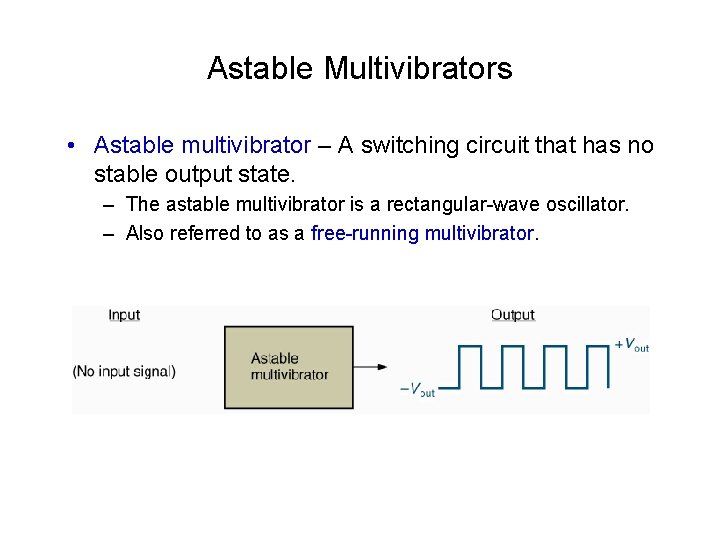
Astable Multivibrators • Astable multivibrator – A switching circuit that has no stable output state. – The astable multivibrator is a rectangular-wave oscillator. – Also referred to as a free-running multivibrator.

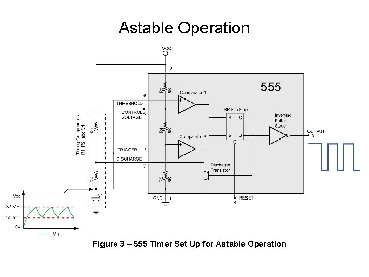
Astable Operation Figure 3 – 555 Timer Set Up for Astable Operation

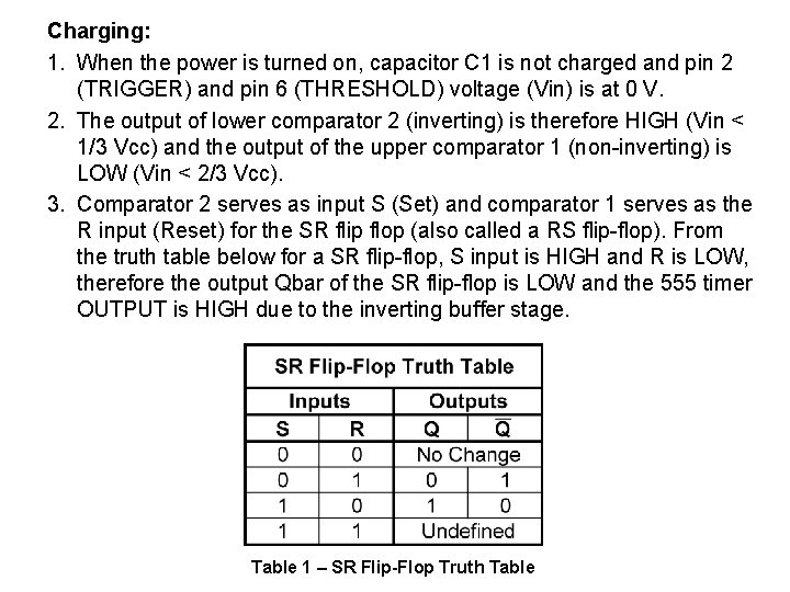
Charging: 1. When the power is turned on, capacitor C 1 is not charged and pin 2 (TRIGGER) and pin 6 (THRESHOLD) voltage (Vin) is at 0 V. 2. The output of lower comparator 2 (inverting) is therefore HIGH (Vin < 1/3 Vcc) and the output of the upper comparator 1 (non-inverting) is LOW (Vin < 2/3 Vcc). 3. Comparator 2 serves as input S (Set) and comparator 1 serves as the R input (Reset) for the SR flip flop (also called a RS flip-flop). From the truth table below for a SR flip-flop, S input is HIGH and R is LOW, therefore the output Qbar of the SR flip-flop is LOW and the 555 timer OUTPUT is HIGH due to the inverting buffer stage. Table 1 – SR Flip-Flop Truth Table

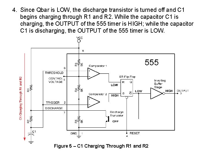
4. Since Qbar is LOW, the discharge transistor is turned off and C 1 begins charging through R 1 and R 2. While the capacitor C 1 is charging, the OUTPUT of the 555 timer is HIGH; while the capacitor C 1 is discharging, the OUTPUT of the 555 timer is LOW. Figure 5 – C 1 Charging Through R 1 and R 2

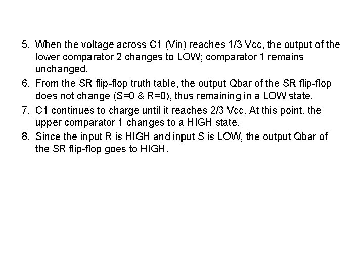
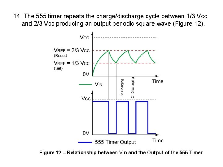
5. When the voltage across C 1 (Vin) reaches 1/3 Vcc, the output of the lower comparator 2 changes to LOW; comparator 1 remains unchanged. 6. From the SR flip-flop truth table, the output Qbar of the SR flip-flop does not change (S=0 & R=0), thus remaining in a LOW state. 7. C 1 continues to charge until it reaches 2/3 Vcc. At this point, the upper comparator 1 changes to a HIGH state. 8. Since the input R is HIGH and input S is LOW, the output Qbar of the SR flip-flop goes to HIGH.

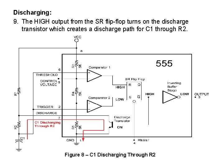
Discharging: 9. The HIGH output from the SR flip-flop turns on the discharge transistor which creates a discharge path for C 1 through R 2. Figure 8 – C 1 Discharging Through R 2

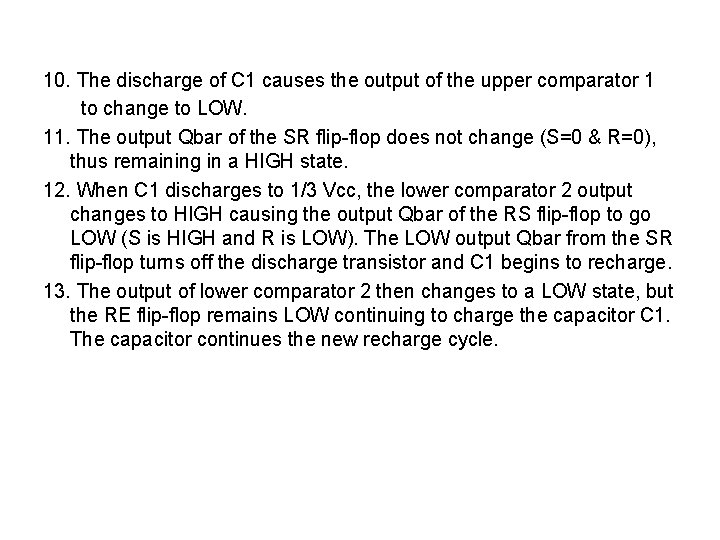
10. The discharge of C 1 causes the output of the upper comparator 1 to change to LOW. 11. The output Qbar of the SR flip-flop does not change (S=0 & R=0), thus remaining in a HIGH state. 12. When C 1 discharges to 1/3 Vcc, the lower comparator 2 output changes to HIGH causing the output Qbar of the RS flip-flop to go LOW (S is HIGH and R is LOW). The LOW output Qbar from the SR flip-flop turns off the discharge transistor and C 1 begins to recharge. 13. The output of lower comparator 2 then changes to a LOW state, but the RE flip-flop remains LOW continuing to charge the capacitor C 1. The capacitor continues the new recharge cycle.

14. The 555 timer repeats the charge/discharge cycle between 1/3 Vcc and 2/3 Vcc producing an output periodic square wave (Figure 12). Figure 12 – Relationship between Vin and the Output of the 555 Timer

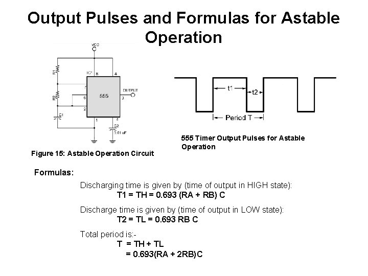
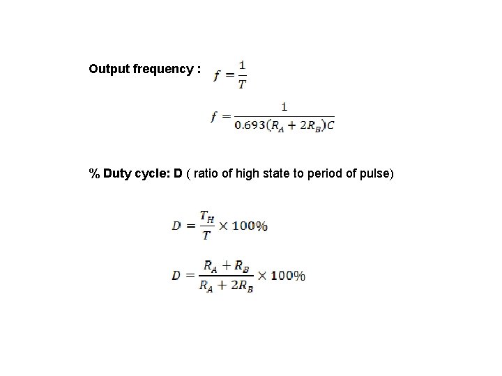
Output Pulses and Formulas for Astable Operation Figure 15: Astable Operation Circuit 555 Timer Output Pulses for Astable Operation Formulas: Discharging time is given by (time of output in HIGH state): T 1 = TH = 0. 693 (RA + RB) C Discharge time is given by (time of output in LOW state): T 2 = TL = 0. 693 RB C Total period is: T = TH + TL = 0. 693(RA + 2 RB)C

Output frequency : % Duty cycle: D ( ratio of high state to period of pulse)

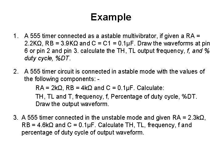
Example 1. A 555 timer connected as a astable multivibrator, if given a RA = 2. 2 KΩ, RB = 3. 9 KΩ and C = C 1 = 0. 1μF. Draw the waveforms at pin 6 or pin 2 and pin 3. calculate the TH, TL output frequency, f, and % duty cycle, %DT. 2. A 555 timer circuit is connected in astable mode with the values of the following components: RA = 2 kΩ, RB = 4 kΩ and C = 0. 1μF. Calculate: TH, TL and T, frequency, f, Percentage of duty cycle, %DT. Draw the output waveform. 3. A 555 timer connected in the unstable mode and given RA = 2. 3 kΩ, RB = 4. 6 kΩ and C = 0. 1μF. Calculate TH, TL, frequency, f and percentage of duty cycle of output waveform.

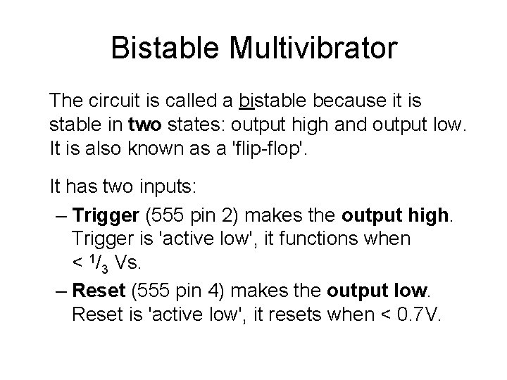
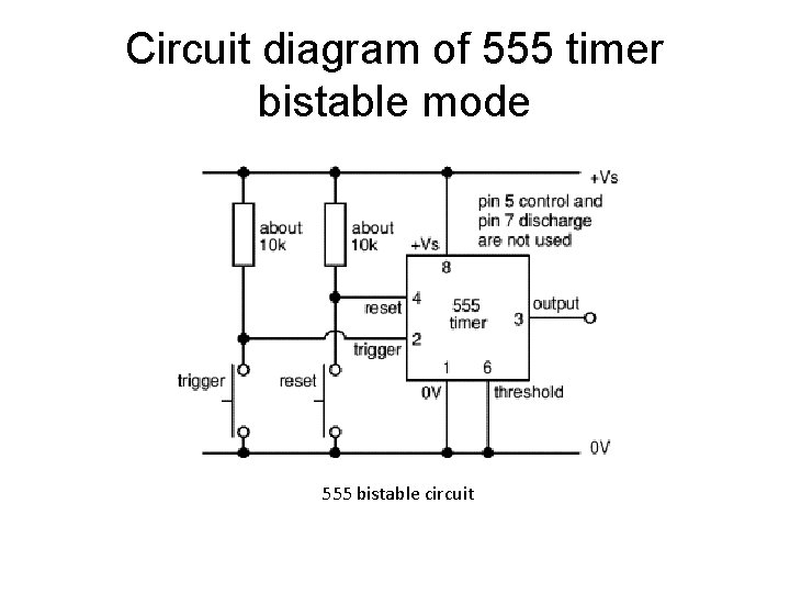
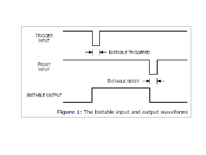
Bistable Multivibrator The circuit is called a bistable because it is stable in two states: output high and output low. It is also known as a 'flip-flop'. It has two inputs: – Trigger (555 pin 2) makes the output high. Trigger is 'active low', it functions when < 1/3 Vs. – Reset (555 pin 4) makes the output low. Reset is 'active low', it resets when < 0. 7 V.

Circuit diagram of 555 timer bistable mode 555 bistable circuit

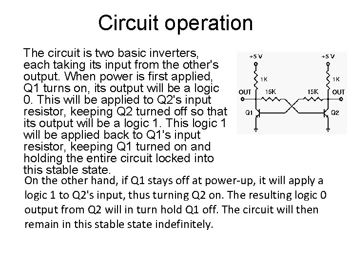
Circuit operation The circuit is two basic inverters, each taking its input from the other's output. When power is first applied, Q 1 turns on, its output will be a logic 0. This will be applied to Q 2's input resistor, keeping Q 2 turned off so that its output will be a logic 1. This logic 1 will be applied back to Q 1's input resistor, keeping Q 1 turned on and holding the entire circuit locked into this stable state. On the other hand, if Q 1 stays off at power-up, it will apply a logic 1 to Q 2's input, thus turning Q 2 on. The resulting logic 0 output from Q 2 will in turn hold Q 1 off. The circuit will then remain in this stable state indefinitely.

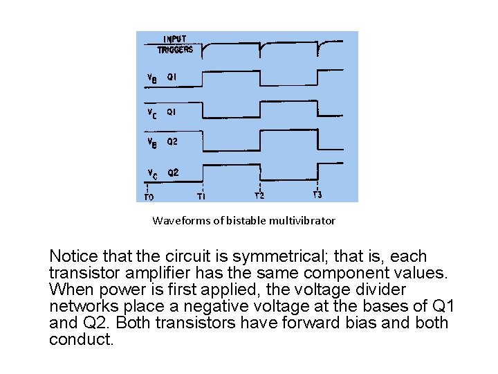
Waveforms of bistable multivibrator Notice that the circuit is symmetrical; that is, each transistor amplifier has the same component values. When power is first applied, the voltage divider networks place a negative voltage at the bases of Q 1 and Q 2. Both transistors have forward bias and both conduct.


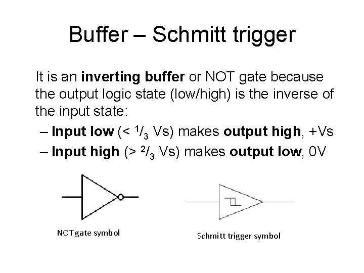
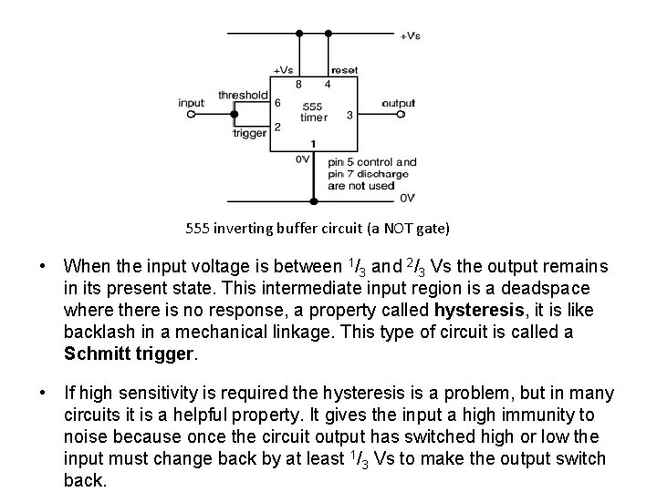
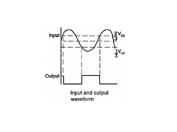
Buffer – Schmitt trigger It is an inverting buffer or NOT gate because the output logic state (low/high) is the inverse of the input state: – Input low (< 1/3 Vs) makes output high, +Vs – Input high (> 2/3 Vs) makes output low, 0 V NOT gate symbol Schmitt trigger symbol

555 inverting buffer circuit (a NOT gate) • When the input voltage is between 1/3 and 2/3 Vs the output remains in its present state. This intermediate input region is a deadspace where there is no response, a property called hysteresis, it is like backlash in a mechanical linkage. This type of circuit is called a Schmitt trigger. • If high sensitivity is required the hysteresis is a problem, but in many circuits it is a helpful property. It gives the input a high immunity to noise because once the circuit output has switched high or low the input must change back by at least 1/3 Vs to make the output switch back.


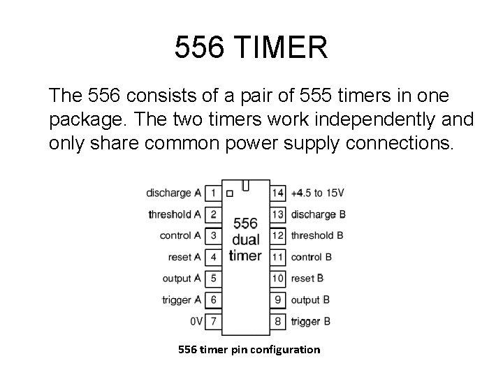
556 TIMER The 556 consists of a pair of 555 timers in one package. The two timers work independently and only share common power supply connections. 556 timer pin configuration