Timers Counters Clock sources ATmega 16 has 3



- Slides: 21

Timers /Counters

Clock sources ► ATmega 16 has 3 timers: timer 0 (8 bit), timer 1 (16 bit) and timer 2 (8 bit). ►Clock sources for these timers/counters are either internal (prescaled clock) or external. ►Timer 0, 1 external clock sources are synchronous produced by edge detection of input signals on pins PB 0, PB 1 sampled once every system clock cycle. On the other hand external clock for timer 2 is asynchronous where a crystal can be connected between the TOSC 1 and TOSC 2 pins (PC 6, PC 7) to serve as an independent clock source that can be prescaled. ►Definitions: Bottom Count = 00 Max Count = FF (or FFFF for timer 1) Top Count = Count at which timer is cleared to zero and is either FF (FFFF) or = Output Compare Register (OCR).

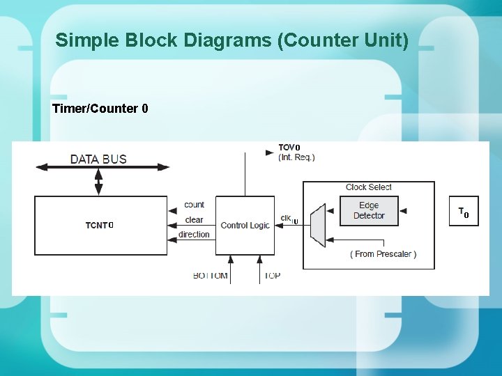
Simple Block Diagrams (Counter Unit) Timer/Counter 0

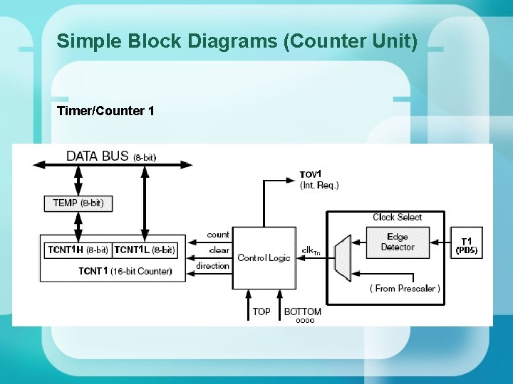
Simple Block Diagrams (Counter Unit) Timer/Counter 1

Timer/Counter 2

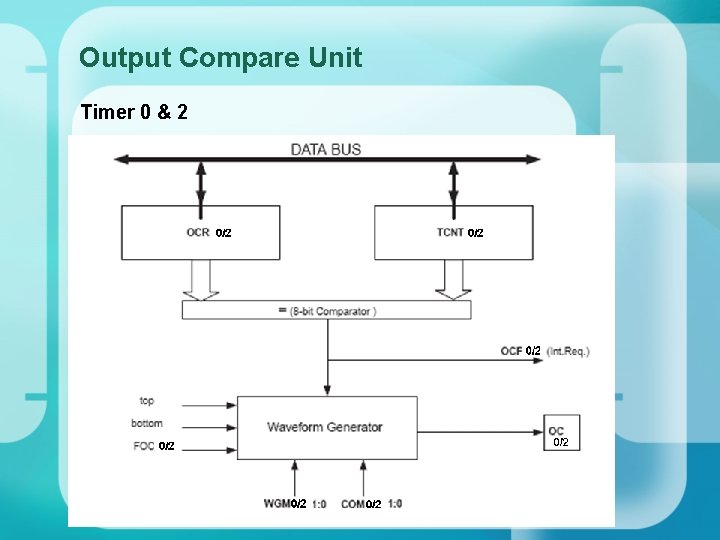
Output Compare Unit Timer 0 & 2

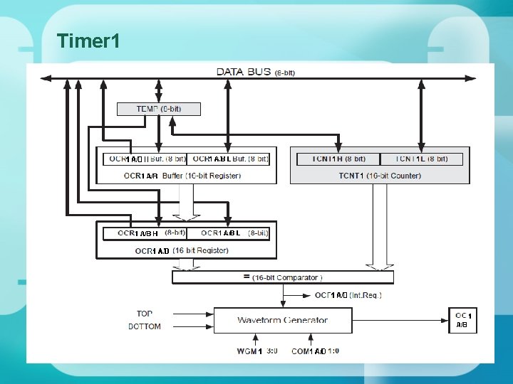
Timer 1

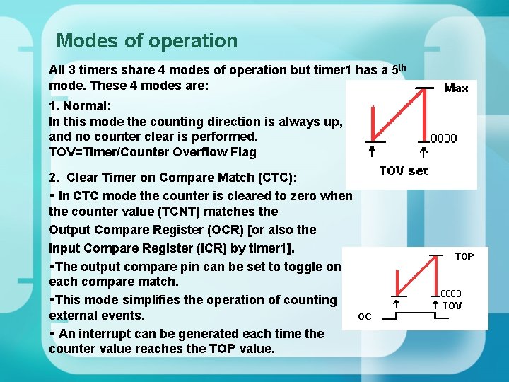
Modes of operation All 3 timers share 4 modes of operation but timer 1 has a 5 th mode. These 4 modes are: 1. Normal: In this mode the counting direction is always up, and no counter clear is performed. TOV=Timer/Counter Overflow Flag 2. Clear Timer on Compare Match (CTC): § In CTC mode the counter is cleared to zero when the counter value (TCNT) matches the Output Compare Register (OCR) [or also the Input Compare Register (ICR) by timer 1]. §The output compare pin can be set to toggle on each compare match. §This mode simplifies the operation of counting external events. § An interrupt can be generated each time the counter value reaches the TOP value.

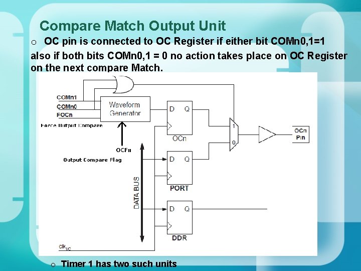
Compare Match Output Unit o OC pin is connected to OC Register if either bit COMn 0, 1=1 also if both bits COMn 0, 1 = 0 no action takes place on OC Register on the next compare Match. o Timer 1 has two such units

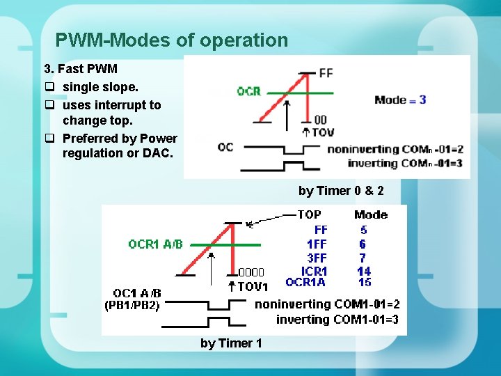
PWM-Modes of operation 3. Fast PWM q single slope. q uses interrupt to change top. q Preferred by Power regulation or DAC. by Timer 0 & 2 by Timer 1

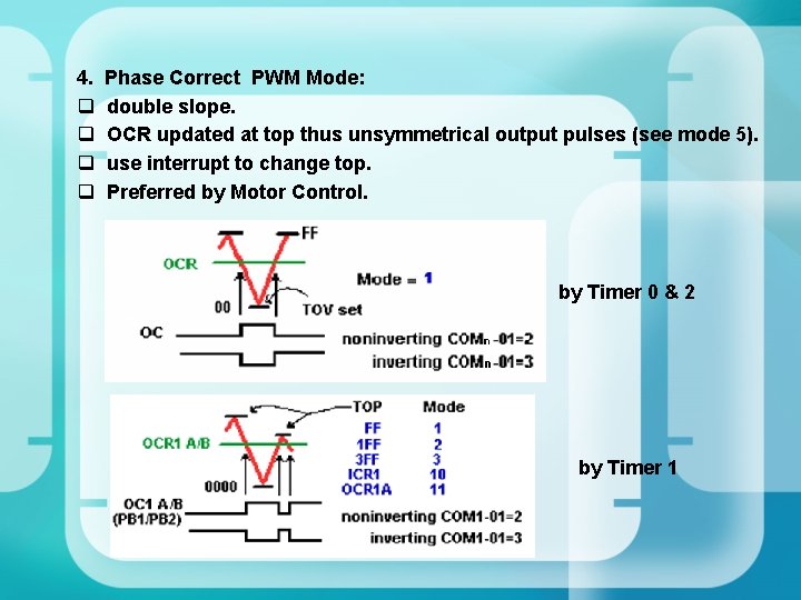
4. q q Phase Correct PWM Mode: double slope. OCR updated at top thus unsymmetrical output pulses (see mode 5). use interrupt to change top. Preferred by Motor Control. by Timer 0 & 2 by Timer 1

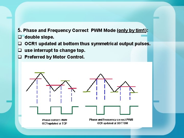
5. Phase and Frequency Correct PWM Mode (only by tim 1): q q double slope. OCR 1 updated at bottom thus symmetrical output pulses. use interrupt to change top. Preferred by Motor Control.

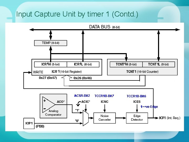
Input Capture Unit by timer 1 • The input Capture unit captures external events and It writes the 16 -bit value of the counter (TCNT 1) to the Input Capture Register (ICR 1), and the Input Capture Flag (ICF 1) is set. • The Noise Canceller function requires four successive equal valued samples of the input for changing its output. Its Output is therefore delayed by four Oscillator cycles. • If enabled, the Input Capture Flag ICF 1 generates an Input Capture interrupt.

Input Capture Unit by timer 1 (Contd. )

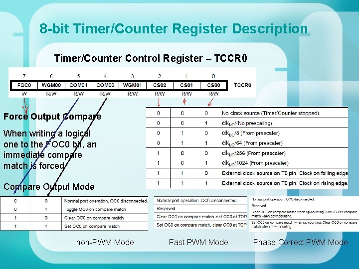
8 -bit Timer/Counter Register Description Timer/Counter Control Register – TCCR 0 Force Output Compare When writing a logical one to the FOC 0 bit, an immediate compare match is forced Compare Output Mode non-PWM Mode Fast PWM Mode Phase Correct PWM Mode

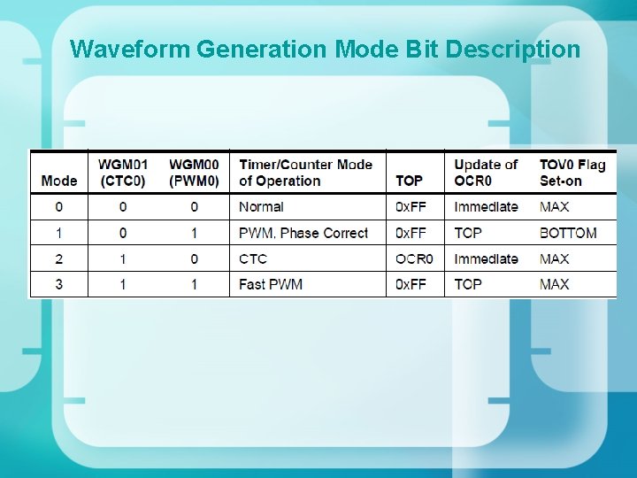
Waveform Generation Mode Bit Description

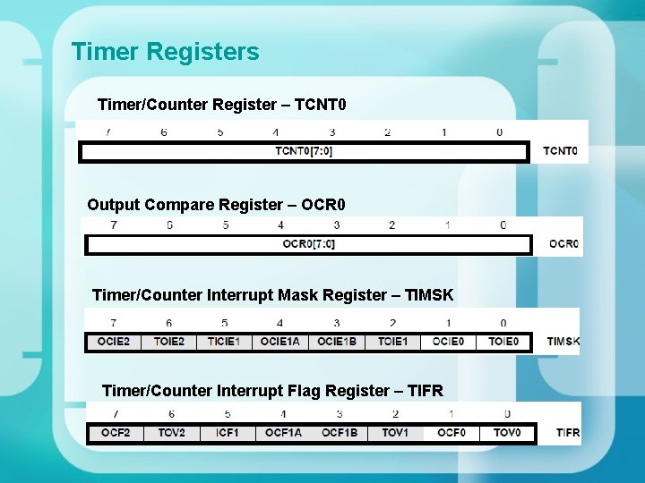
Timer Registers Timer/Counter Register – TCNT 0 Output Compare Register – OCR 0 Timer/Counter Interrupt Mask Register – TIMSK Timer/Counter Interrupt Flag Register – TIFR

Accessing 16 -bit Registers by timer 1 • The TCNT 1, OCR 1 A/B, and ICR 1 are 16 -bit registers. • The 16 -bit register must be byte accessed using two read or write operations. • A temporary storage register is shared between all 16 bit registers. • Accessing the Low byte triggers the 16 -bit read or write operation. When the Low byte of a 16 -bit register is written by the CPU, the High byte stored in the temporary register, and the Low byte written are both copied into the 16 -bit register in the same clock cycle. • Also when the Low byte of a 16 -bit register is read by the CPU, the High byte of the 16 -bit register is copied into the temporary register in the same clock cycle as the Low byte is read.

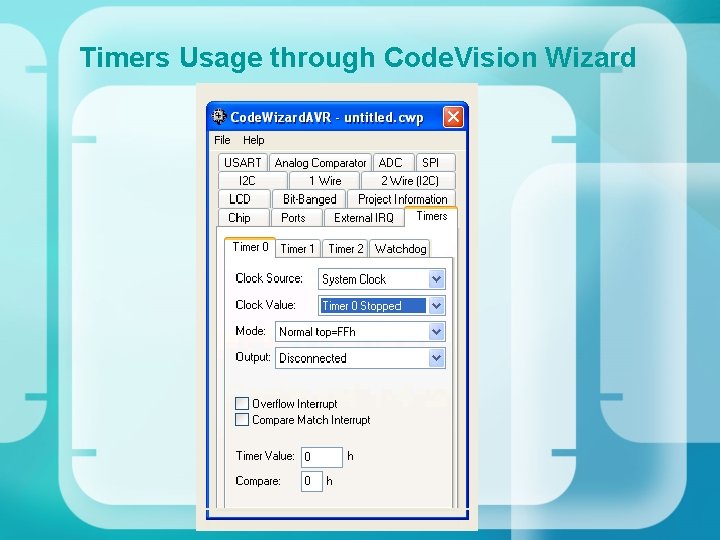
Timers Usage through Code. Vision Wizard

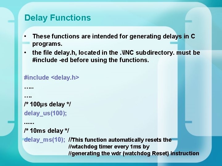
Delay Functions • These functions are intended for generating delays in C programs. • the file delay. h, located in the. INC subdirectory. must be #include -ed before using the functions. #include <delay. h> …. /* 100μs delay */ delay_us(100); . . . /* 10 ms delay */ delay_ms(10); //This function automatically resets the //wtachdog timer every 1 ms by //generating the wdr (watchdog Reset) instruction
