Time Pix 3 status and protection Yevgen Bilevych

Time. Pix 3 status and protection Yevgen Bilevych Amsterdam 13. 10. 2015

Main technological steps for the formation of structure Time. Pix / SU-8 / Al grid 1. Formation of protection layer 2. Deposition of SU-8 3. Aluminum deposition 4. Formation of structure “support” / grid

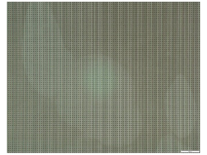
Time. Pix 3 16210 mm 16120 mm Time. Pix 14111 mm 14110 mm 107 single chips 105 single chips Surface materials: - Aluminum (aluminum oxide) - Silicon nitride - Silicon oxide - Thickness 725 µm

Protection layer formation Time. Pix 3

TPX 3 Polyimide mask

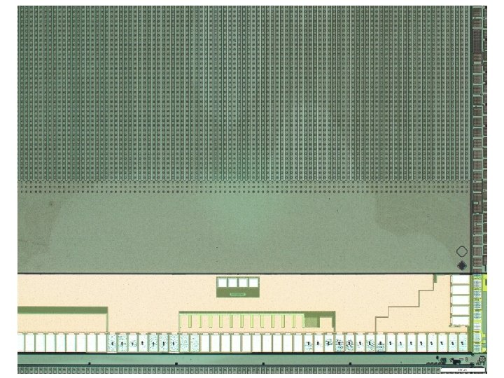
Dykes shape, size and location Time. Pix 3 16210 mm 16120 mm Time. Pix 14111 mm lost area ~ 9, 4% 14100 mm lost area ~ 3, 1%

Time. Pix 3

Time. Pix 3/SU-8 dykes

Time. Pix 3
")
Time. Pix 3/SU-8 dykes (top and side)

Time. Pix 3
")
Time. Pix 3/SU-8 dykes (bottom and side)

Time. Pix 3
")
Time. Pix 3/SU-8 dykes (side)

TPX 3 SU-8 mask

Time. Pix 3/SU-8 dykes/Al grid

Time. Pix 3/SU-8 dykes/Al grid

Time. Pix 3/SU-8 dykes/Al grid

Time. Pix 3/SU-8 dykes/Al grid

TPX 3 Al grid mask

TPX 3 Bottom electrode mask

Two critical points Protection layer formation Alta. CVD cluster line Al layer deposition Eva. Tec CLUSTERLINE® 200

Time. Pix W 0064 EN 5 MX 1 X High pressure water jet O 2 plasma HNO 3 fuming

Time. Pix W 0065 EX 5 MVTX High pressure water jet O 2 plasma

W 0064 W 0065

Initial wafer surface preparation!!!

No delay after Al deposition!!!
 Complete")
Plans Silicon nitride deposition onto W 0066 EV 5 MWCX (55 A-type chips) Complete test run with TPX 3 masks set TPX 3 (Wafer 15) / In. Grid run
- Slides: 30