Threshold Shift vs Gate Oxide Thickness Poly Si

- Slides: 13

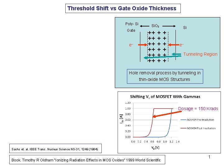
Threshold Shift vs Gate Oxide Thickness Poly- Si Gate e-- Si. O 2 ++ ++ ++ + + + Si e-Tunneling Region Hole removal process by tunneling in thin-oxide MOS Structures Dosage = 150 Krads Sachs et. al. IEEE Trans. Nuclear Science NS-31, 1249 (1984) Book. Timothy R Oldham “Ionizing Radiation Effects in MOS Oxides” 1999 World Scientific 1

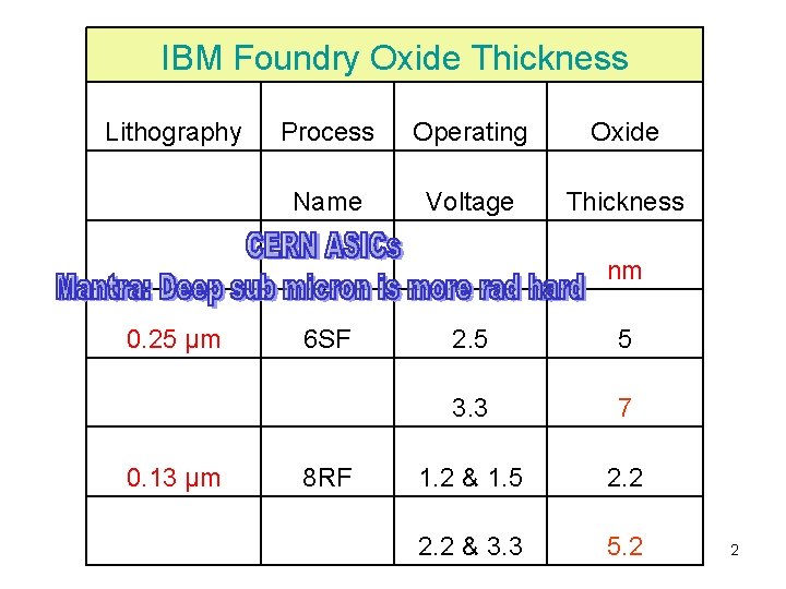
IBM Foundry Oxide Thickness Lithography Process Operating Oxide Name Voltage Thickness 0. 25 µm 0. 13 µm nm 6 SF 2. 5 5 3. 3 7 8 RF 1. 2 & 1. 5 2. 2 & 3. 3 5. 2 2

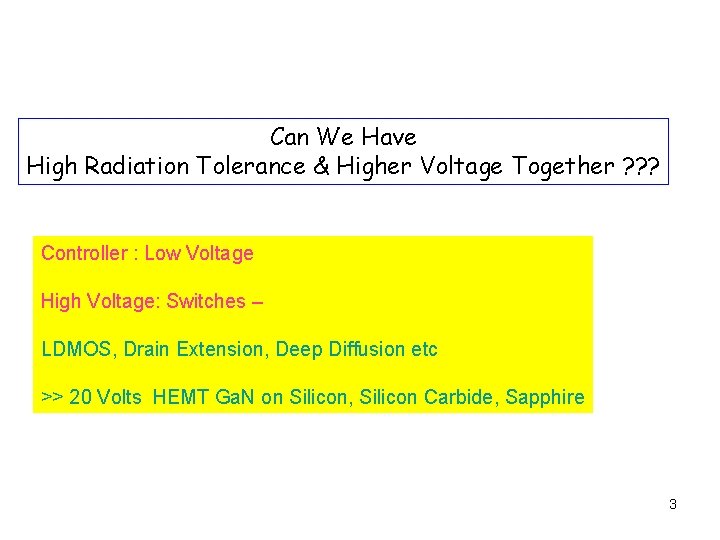
Can We Have High Radiation Tolerance & Higher Voltage Together ? ? ? Controller : Low Voltage High Voltage: Switches – LDMOS, Drain Extension, Deep Diffusion etc >> 20 Volts HEMT Ga. N on Silicon, Silicon Carbide, Sapphire 3

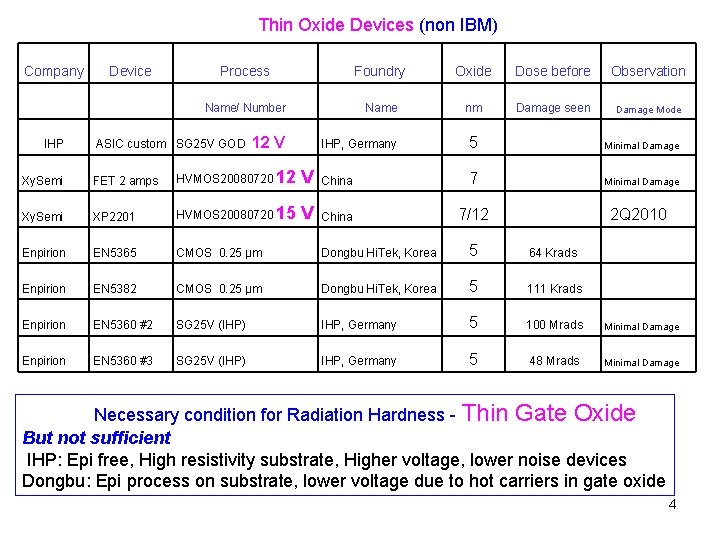
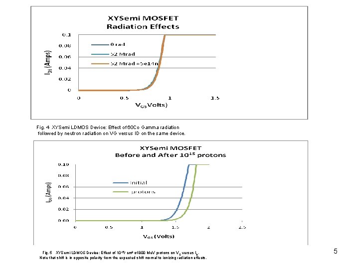
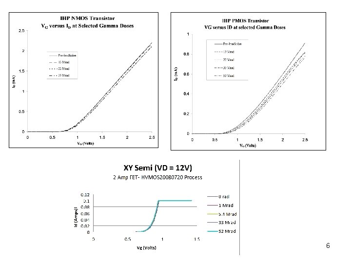
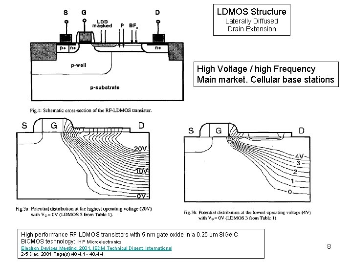
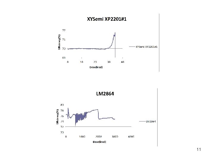
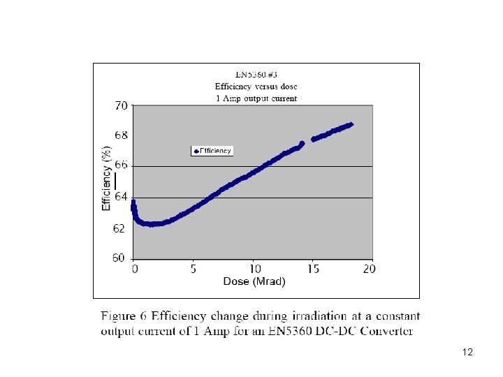
Thin Oxide Devices (non IBM) Company Device IHP Process Foundry Oxide Dose before Observation Name/ Number Name nm Damage seen Damage Mode ASIC custom SG 25 V GOD 12 V IHP, Germany 5 Minimal Damage Xy. Semi FET 2 amps HVMOS 20080720 12 V China 7 Minimal Damage Xy. Semi XP 2201 HVMOS 20080720 15 V China 7/12 Enpirion EN 5365 CMOS 0. 25 µm Dongbu Hi. Tek, Korea 5 64 Krads Enpirion EN 5382 CMOS 0. 25 µm Dongbu Hi. Tek, Korea 5 111 Krads Enpirion EN 5360 #2 SG 25 V (IHP) IHP, Germany 5 100 Mrads Minimal Damage Enpirion EN 5360 #3 SG 25 V (IHP) IHP, Germany 5 48 Mrads Minimal Damage 2 Q 2010 Necessary condition for Radiation Hardness - Thin Gate Oxide But not sufficient IHP: Epi free, High resistivity substrate, Higher voltage, lower noise devices Dongbu: Epi process on substrate, lower voltage due to hot carriers in gate oxide 4

Fig. 4 XYSemi LDMOS Device: Effect of 60 Co Gamma radiation followed by neutron radiation on VG versus ID on the same device. Fig. 5 XYSemi LDMOS Device: Effect of 10 15/ cm 2 of 800 Me. V protons on V G versus ID. Note that shift is in opposite polarity from the expected shift normal to ionizing radiation effects. 5

6

Twepp Nagos 7

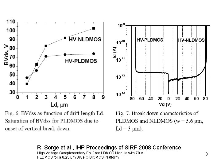
LDMOS Structure Laterally Diffused Drain Extension High Voltage / high Frequency Main market. Cellular base stations High performance RF LDMOS transistors with 5 nm gate oxide in a 0. 25 μm Si. Ge: C Bi. CMOS technology: IHP Microelectronics Electron Devices Meeting, 2001. IEDM Technical Digest. International 2 -5 Dec. 2001 Page(s): 40. 4. 1 - 40. 4. 4 8

R. Sorge et al , IHP Proceedings of SIRF 2008 Conference High Voltage Complementary Epi Free LDMOS Module with 70 V PLDMOS for a 0. 25 μm Si. Ge: C Bi. CMOS Platform 9

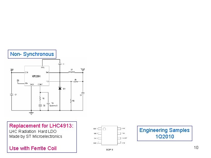
Non- Synchronous Replacement for LHC 4913: LHC Radiation Hard LDO Made by ST Microelectronics Use with Ferrite Coil Engineering Samples 1 Q 2010 10

11

12

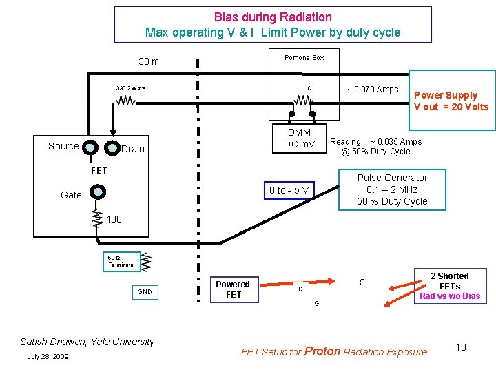
Bias during Radiation Max operating V & I Limit Power by duty cycle Pomona Box 30 m 330 2 Watts Source ~ 0. 070 Amps 1 Ω DMM DC m. V Drain FET Reading = ~ 0. 035 Amps @ 50% Duty Cycle Pulse Generator 0. 1 – 2 MHz 50 % Duty Cycle 0 to - 5 V Gate Power Supply V out = 20 Volts 100 50 Ω. Terminator GND Powered FET S D G Satish Dhawan, Yale University July 28. 2009 2 Shorted FETs Rad vs wo Bias FET Setup for Proton Radiation Exposure 13