This week Layout and fabrication of CMOS circuits
This week Layout and fabrication of CMOS circuits After an idea from Peter. Nilsson@es. lth. se

CMOS technology Fabrication of CMOS circuits A short introductory review After an idea from Peter. Nilsson@es. lth. se
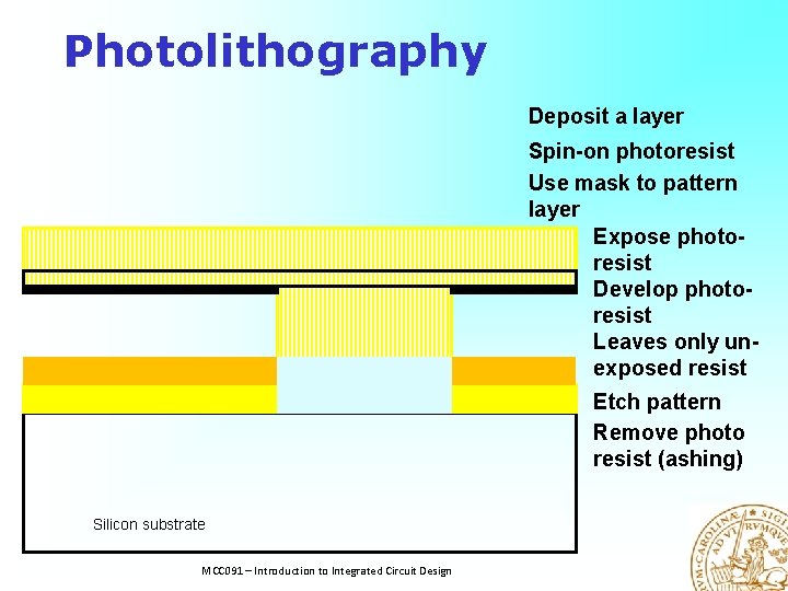
Photolithography Deposit a layer Spin-on photoresist Use mask to pattern layer Expose photoresist Develop photoresist Leaves only unexposed resist Etch pattern Remove photo resist (ashing) Silicon substrate MCC 091 – Introduction to Integrated Circuit Design
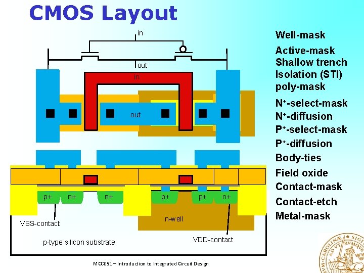
CMOS Layout in Well-mask out Active-mask Shallow trench Isolation (STI) poly-mask in VSS VDD N+-select-mask N+-diffusion P+-select-mask P+-diffusion Body-ties Field oxide Contact-mask out p+ n+ n+ p+ p+ n+ n-well VSS-contact p-type silicon substrate VDD-contact MCC 091 – Introduction to Integrated Circuit Design Contact-etch Metal-mask
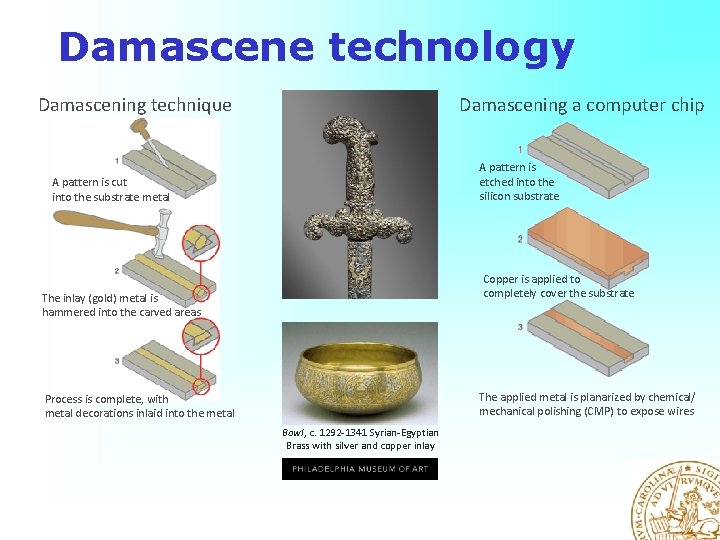
Damascene technology Damascening a computer chip Damascening technique A pattern is etched into the silicon substrate A pattern is cut into the substrate metal Copper is applied to completely cover the substrate The inlay (gold) metal is hammered into the carved areas The applied metal is planarized by chemical/ mechanical polishing (CMP) to expose wires Process is complete, with metal decorations inlaid into the metal Bowl, c. 1292 -1341 Syrian-Egyptian Brass with silver and copper inlay
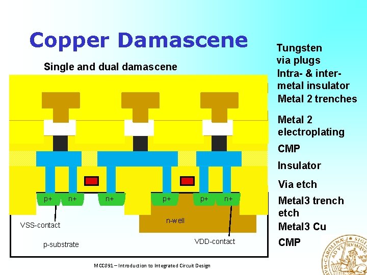
Copper Damascene Single and dual damascene Tungsten via plugs Intra- & intermetal insulator Metal 2 trenches Metal 2 electroplating CMP Insulator Via etch p+ n+ VSS-contact p-substrate n+ p+ p+ n+ n-well VDD-contact MCC 091 – Introduction to Integrated Circuit Design Metal 3 trench etch Metal 3 Cu CMP
- Slides: 6