This file contains a block diagram and some
This file contains a block diagram and some functional notes on the L 2 Beta 9 U card design. Results of discussions among Philippe Cros, Drew Baden, and Bob Hirosky are merged into the design. Base design uses an Altera 20 K 200 FPGA and PLX 9054 PCI interface The choice of the Altera will expedite our firmware development cycle. The choice of the PLX chip will give our design greater flexibility, because the PLX supports both 3. 3 V and 5 V PCI buses. Use of a commercial PCI interface will also reduce our firmware complexity. Details of the mechanical design are show in talks by Philippe Cros.
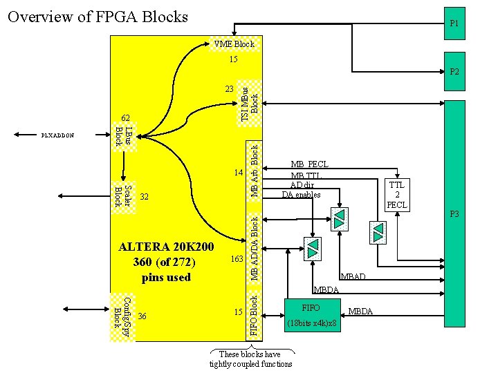
Overview of FPGA Blocks P 1 VME Block 15 LBus Block 14 Scaler Block 32 ALTERA 20 K 200 360 (of 272) pins used 163 MB_PECL MB TTL AD dir DA enables TTL 2 PECL MBAD MBDA Config/Spy Block 36 15 FIFO Block PLX ADDON MB Arb. Block 62 MB AD/DA Block 23 TSI MBus Block P 2 FIFO (18 bits x 4 k)x 8 These blocks have tightly coupled functions MBDA P 3
![Add-on bus block Fixed by AMCC SPECS Add-on bus 62 signals DQ[31: 0] BP_CLK Add-on bus block Fixed by AMCC SPECS Add-on bus 62 signals DQ[31: 0] BP_CLK](http://slidetodoc.com/presentation_image/220b34616c4f08781408bb1a712d32e5/image-3.jpg)
Add-on bus block Fixed by AMCC SPECS Add-on bus 62 signals DQ[31: 0] BP_CLK IRQ* SYSRST* ADR[6: 2] BE[3: 0]* SELECT* WR* RD* PT_NUM[1: 0] PTBE[3: 0]* PTATN* PTBURST* PTADR* PTWR PTRDY* WRFULL WRFIFO* RDEMPTY RDFIFO*
![VME block P 1 6 signals Config. /SPY block GAP* GA[4: 0]* JTAG/EPROM/DIAGNOSTIC I/O, VME block P 1 6 signals Config. /SPY block GAP* GA[4: 0]* JTAG/EPROM/DIAGNOSTIC I/O,](http://slidetodoc.com/presentation_image/220b34616c4f08781408bb1a712d32e5/image-4.jpg)
VME block P 1 6 signals Config. /SPY block GAP* GA[4: 0]* JTAG/EPROM/DIAGNOSTIC I/O, etc P 2 9 signals SCL_INT/Worker_int L 2 Answer Ready VBD_DONE VBD_Start_Request/VBD_START J 2_Test_Out(0)/Worker 1_Int J 2_Test_Out(1)/Worker 2_Int Worker 3_Int Worker 4_Int Worker 5_Int 36 signals Clock Reset EPROM[5] JTAG[5]? Logic Analyzer[16] Switches[4] LED DISPLAY[4]?
![TSI MBus+scalar block 55 signals MOD_DONE[15] EV_LOADED[3] START_LOAD DONE_OUT MB_RESET AP_FIFO_EMPTY ECL SALERS[32] VME TSI MBus+scalar block 55 signals MOD_DONE[15] EV_LOADED[3] START_LOAD DONE_OUT MB_RESET AP_FIFO_EMPTY ECL SALERS[32] VME](http://slidetodoc.com/presentation_image/220b34616c4f08781408bb1a712d32e5/image-5.jpg)
TSI MBus+scalar block 55 signals MOD_DONE[15] EV_LOADED[3] START_LOAD DONE_OUT MB_RESET AP_FIFO_EMPTY ECL SALERS[32] VME block (signals on P 1&P 2) P 1 6 signals P 2 9 signals GA[5: 0]* SCL_INT/Worker_int L 2 Answer Ready VBD_DONE VBD_Start_Request/VBD_START J 2_Test_Out(0)/Worker 1_Int J 2_Test_Out(1)/Worker 2_Int Worker 3_Int Worker 4_Int Worker 5_Int “MISC” out: EV_LOADED[3: 0], START_LOAD, DONE_OUT, MB_RESET, AP_FIFO_EMPTY
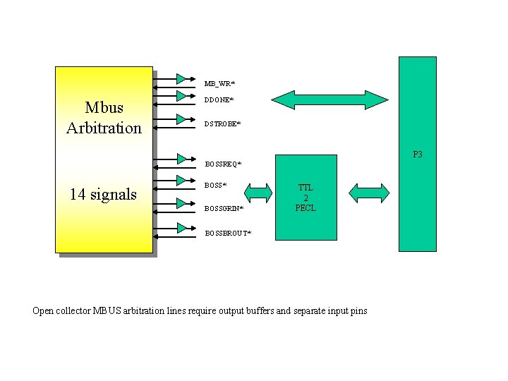
MB_WR* Mbus Arbitration DDONE* DSTROBE* P 3 BOSSREQ* 14 signals BOSS* BOSSGRIN* TTL 2 PECL BOSSBROUT* Open collector MBUS arbitration lines require output buffers and separate input pins
![MBUS AD/DA + FIFO block AD_DIR AD[32] OE PIO_OUT DA[128] FPGA 188 Pins used MBUS AD/DA + FIFO block AD_DIR AD[32] OE PIO_OUT DA[128] FPGA 188 Pins used](http://slidetodoc.com/presentation_image/220b34616c4f08781408bb1a712d32e5/image-7.jpg)
MBUS AD/DA + FIFO block AD_DIR AD[32] OE PIO_OUT DA[128] FPGA 188 Pins used P 3 OE PIO_IN WCLK, WEN RCLK, REN, OE EF, FF MB DMA AD[10] FIFO (18 bits x 4 k)x 8
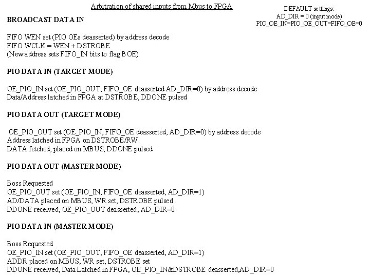
Arbitration of shared inputs from Mbus to FPGA BROADCAST DATA IN DEFAULT settings: AD_DIR = 0 (input mode) PIO_OE_IN=PIO_OE_OUT=FIFO_OE=0 FIFO WEN set (PIO OEs deasserted) by address decode FIFO WCLK = WEN + DSTROBE (New address sets FIFO_IN bits to flag BOE) PIO DATA IN (TARGET MODE) OE_PIO_IN set (OE_PIO_OUT, FIFO_OE deasserted AD_DIR=0) by address decode Data/Address latched in FPGA at DSTROBE, DDONE pulsed PIO DATA OUT (TARGET MODE) OE_PIO_OUT set (OE_PIO_IN, FIFO_OE deasserted, AD_DIR=0) by address decode Address latched in FPGA on DSTROBE/RW DATA fetched, placed on MBUS, DDONE pulsed PIO DATA OUT (MASTER MODE) Boss Requested OE_PIO_OUT set (OE_PIO_IN, FIFO_OE deasserted, AD_DIR=1) AD/DATA placed on MBUS, WR set, DSTROBE pulsed DDONE received, OE_PIO_OUT deasserted, AD_DIR=0 PIO DATA IN (MASTER MODE) Boss Requested OE_PIO_IN set (OE_PIO_OUT, FIFO_OE deasserted, AD_DIR=1) ADDR placed on MBUS, WR set, DSTROBE set DDONE received, Data Latched in FPGA, OE_PIO_IN&DSTROBE deasserted, AD_DIR=0
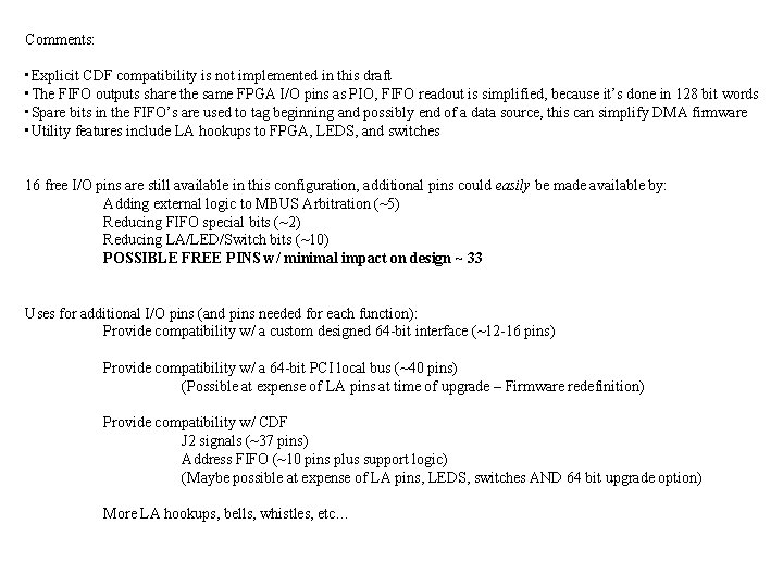
Comments: • Explicit CDF compatibility is not implemented in this draft • The FIFO outputs share the same FPGA I/O pins as PIO, FIFO readout is simplified, because it’s done in 128 bit words • Spare bits in the FIFO’s are used to tag beginning and possibly end of a data source, this can simplify DMA firmware • Utility features include LA hookups to FPGA, LEDS, and switches 16 free I/O pins are still available in this configuration, additional pins could easily be made available by: Adding external logic to MBUS Arbitration (~5) Reducing FIFO special bits (~2) Reducing LA/LED/Switch bits (~10) POSSIBLE FREE PINS w/ minimal impact on design ~ 33 Uses for additional I/O pins (and pins needed for each function): Provide compatibility w/ a custom designed 64 -bit interface (~12 -16 pins) Provide compatibility w/ a 64 -bit PCI local bus (~40 pins) (Possible at expense of LA pins at time of upgrade – Firmware redefinition) Provide compatibility w/ CDF J 2 signals (~37 pins) Address FIFO (~10 pins plus support logic) (Maybe possible at expense of LA pins, LEDS, switches AND 64 bit upgrade option) More LA hookups, bells, whistles, etc…
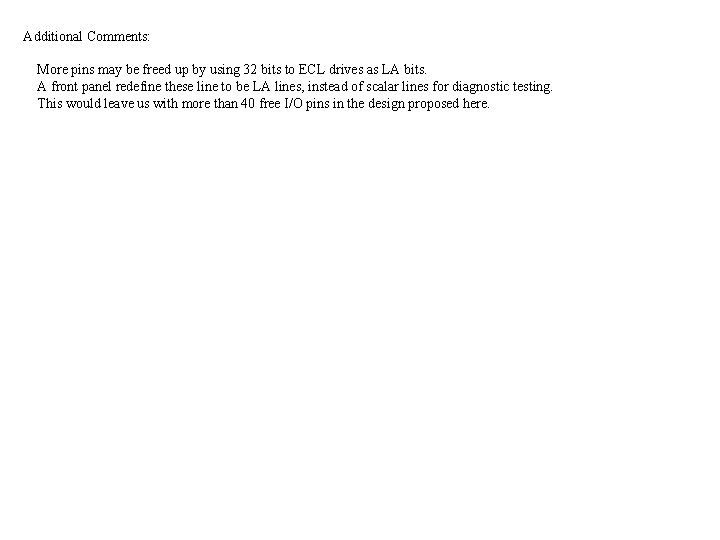
Additional Comments: More pins may be freed up by using 32 bits to ECL drives as LA bits. A front panel redefine these line to be LA lines, instead of scalar lines for diagnostic testing. This would leave us with more than 40 free I/O pins in the design proposed here.
- Slides: 10