Third Class Real Time System Design Output Interfacing

- Slides: 16

Third Class Real Time System Design Output Interfacing Asst. Lec. Lubna A. Alnabi

Output Interfacing This type of interfacing is used to output the data from data bus to the external devices connected to the controlling system. One of the interfacing components is the D-flip flop In electronics, a flip-flop is a circuit that has two stable states and can be used to store state information. The circuit can be made to change state by signals applied to one or more control inputs and will have one or two outputs. Flip-flops are a fundamental building block of digital electronics systems used in computers, communications, and many other types of systems.

Output Interfacing Flip-flops and latches are used as data storage elements. A flip-flop stores a single bit (binary digit) of data; one of its two states represents a "one" and the other represents a "zero". When used some systems, the output and next state depend not only on its current input, but also on its current state (and hence, previous inputs).

Output Interfacing Buffers and latches are used to construct input and output interfacing devices. The latches such as 74 LS 374 are used to latch and hold data for input data to the controller and output to the external devices. The other job of the latch is to protect the controller in case of any short might happen to the external devices which might destroy the controller circuitry.

I/O Interfacing Tri-state Buffers are available in integrated circuits form as octal buffer/drivers in both unidirectional and bi-directional forms, with the more common being the TTL 74240, the TTL 74244 and the TTL 74245.

The most commonly available Digital Buffer and Tri-state Buffer IC’s include: • 74 LS 07 Hex Non-inverting Buffer. • 74 LS 17 Hex Buffer/Driver. • 74 LS 244 Octal Buffer/Line Driver. • 74 LS 245 Octal Bi-directional Buffer.

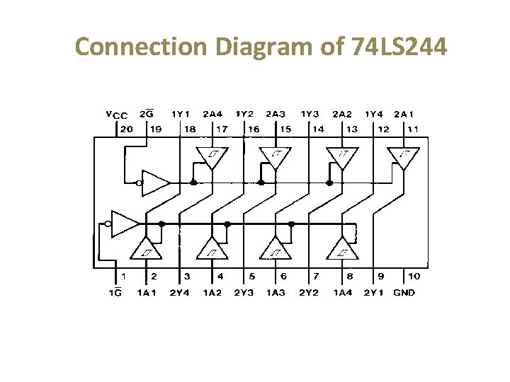
74 LS 244 Octal 3 -State Buffer/Line Driver/Line Receiver The 74 LS 244 buffer/line driver is designed to improve the performance of 3 - State buffers/ drivers plus to provide improved noise rejection. In electronics, a driver is an electrical circuit or other electronic component used to control another circuit or component, such as a high-power transistor, liquid crystal display (LCD), and numerous others.

Features of 74 LS 244 • 3 -State outputs drive bus lines. • PNP inputs reduce DC loading on bus lines. • Improves noise rejection. • Typical IOL (sink current) 24 m. A. • Typical IOH (source current) -15 m. A. • Typical enable/disable time 18 ns.

Connection Diagram of 74 LS 244

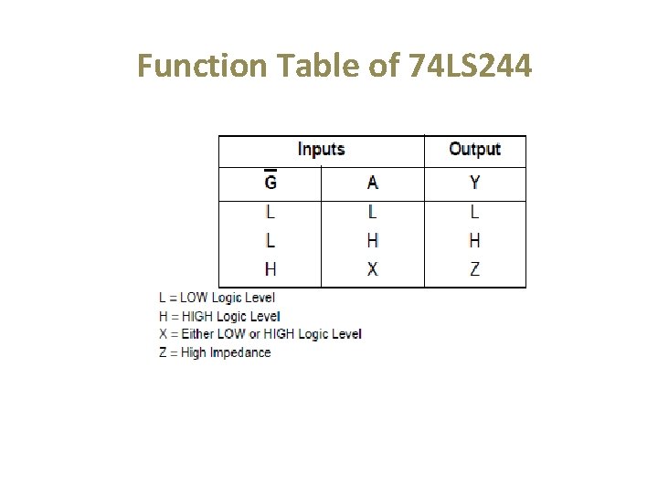
Function Table of 74 LS 244

Absolute Maximum Ratings are those values beyond which the safety of the device cannot be guaranteed. The device should not be operated at these limits.

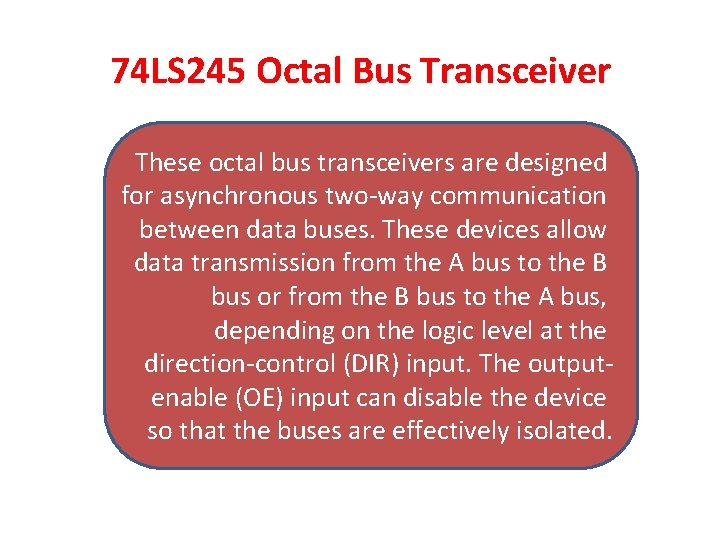
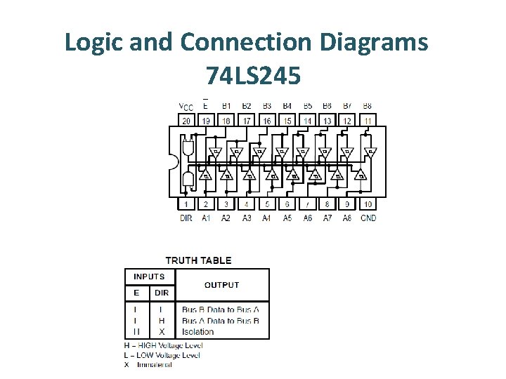
74 LS 245 Octal Bus Transceiver These octal bus transceivers are designed for asynchronous two-way communication between data buses. These devices allow data transmission from the A bus to the B bus or from the B bus to the A bus, depending on the logic level at the direction-control (DIR) input. The outputenable (OE) input can disable the device so that the buses are effectively isolated.

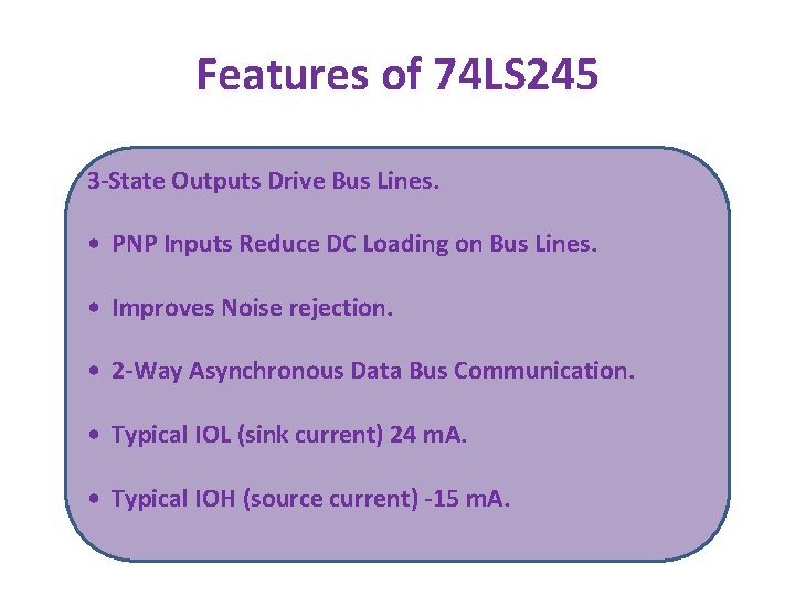
Features of 74 LS 245 3 -State Outputs Drive Bus Lines. • PNP Inputs Reduce DC Loading on Bus Lines. • Improves Noise rejection. • 2 -Way Asynchronous Data Bus Communication. • Typical IOL (sink current) 24 m. A. • Typical IOH (source current) -15 m. A.

Logic and Connection Diagrams 74 LS 245

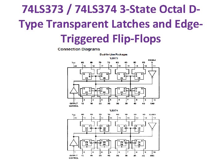
74 LS 373 / 74 LS 374 3 -State Octal DType Transparent Latches and Edge. Triggered Flip-Flops The 74 LS 37 X (3, 4) consists of eight registers (latches, flip flop) with 3 -state outputs. The eight latches of the 74 LS 373 are D-type latches meaning that while the enable (G) is high the Q outputs will follow the data (D) inputs. When the enable is taken low the output will be latched at the level of the data that was set up.

74 LS 373 / 74 LS 374 3 -State Octal DType Transparent Latches and Edge. Triggered Flip-Flops