thin single crystal diamond detectorscharacterization and synchrotron applications
![e 6 CVD material, bulk crystal lattice defects [1, 0, 0] CVD grown diamond e 6 CVD material, bulk crystal lattice defects [1, 0, 0] CVD grown diamond](https://slidetodoc.com/presentation_image_h/016a733dcdaeb70ca939a4d2d62fcec3/image-10.jpg)
![scaife abrasive polishing variability: e 6 sinhgle crystal CVD [100], laser ‘breadsliced’ into two scaife abrasive polishing variability: e 6 sinhgle crystal CVD [100], laser ‘breadsliced’ into two](https://slidetodoc.com/presentation_image_h/016a733dcdaeb70ca939a4d2d62fcec3/image-16.jpg)


![e 6 CVD sample variability polarized light transmission parallel to [100], 350µm thick plates e 6 CVD sample variability polarized light transmission parallel to [100], 350µm thick plates](https://slidetodoc.com/presentation_image_h/016a733dcdaeb70ca939a4d2d62fcec3/image-35.jpg)
- Slides: 37

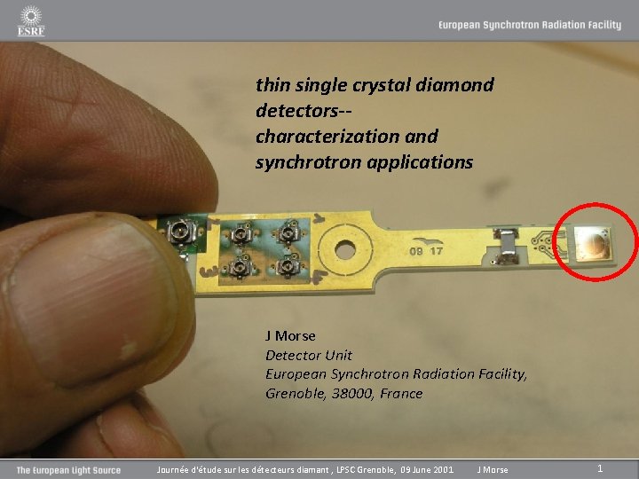
thin single crystal diamond detectors-characterization and synchrotron applications J Morse Detector Unit European Synchrotron Radiation Facility, Grenoble, 38000, France Journée d'étude sur les détecteurs diamant , LPSC Grenoble, 09 June 2001 J Morse 1

Outline basics-1. synchrotron X-ray beam monitoring: why diamond? 2. diamond materials: polycrystalline, hetero-growth, and single crystal 3. (CVD) single crystal diamond: bulk- and surface- defects applications- 4. quadrant electrode beam position monitors with electrometer and RF readout; fast timing application 5. Below 50µm, the 'superthinning’ challenge 6. Conclusions Journée d'étude sur les détecteurs diamant , LPSC Grenoble, 09 June 2001 J Morse 2

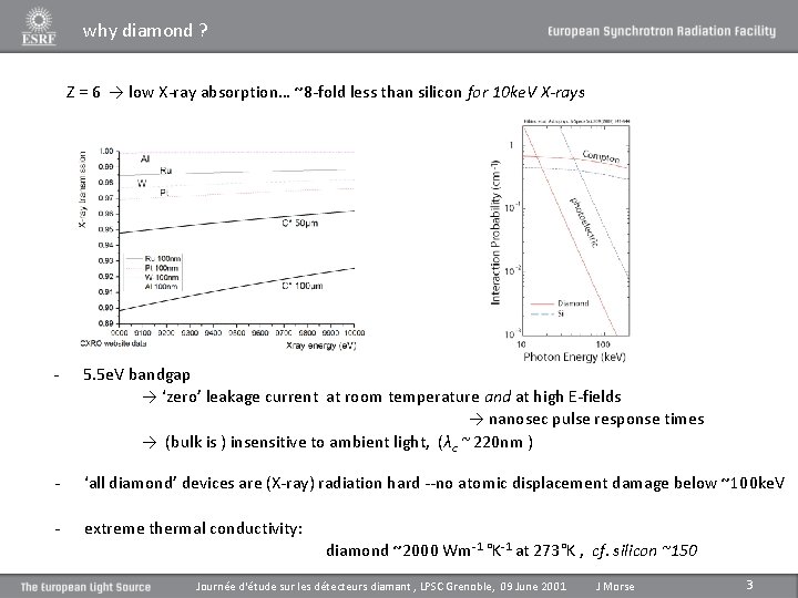
why diamond ? Z = 6 → low X-ray absorption… ~8 -fold less than silicon for 10 ke. V X-rays - 5. 5 e. V bandgap → ‘zero’ leakage current at room temperature and at high E-fields → nanosec pulse response times → (bulk is ) insensitive to ambient light, (λc ~ 220 nm ) - ‘all diamond’ devices are (X-ray) radiation hard --no atomic displacement damage below ~100 ke. V - extreme thermal conductivity: diamond ~2000 Wm-1 °K-1 at 273°K , cf. silicon ~150 Journée d'étude sur les détecteurs diamant , LPSC Grenoble, 09 June 2001 J Morse 3

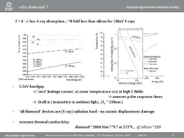
why diamond ? Z = 6 → low X-ray absorption… ~8 -fold less than silicon for 10 ke. V X-rays - 5. 5 e. V bandgap → ‘zero’ leakage current at room temperature and at high E-fields → nanosec pulse response times → (bulk is ) insensitive to ambient light, (λc ~ 220 nm ) - ‘all diamond’ devices are (X-ray) radiation hard --no atomic displacement damage - extreme thermal conductivity: diamond ~2000 Wm-1 °K-1 at 273°K , cf. silicon ~150 Journée d'étude sur les détecteurs diamant , LPSC Grenoble, 09 June 2001 J Morse 4

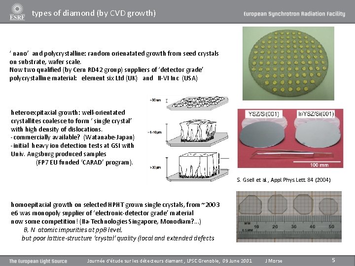
types of diamond (by CVD growth) ‘ nano’ and polycrystalline: random orienatated growth from seed crystals on substrate, wafer scale. Now two qualified (by Cern RD 42 group) suppliers of ‘detector grade’ polycrystalline material: element six Ltd (UK) and II-VI Inc (USA) heteroexpitaxial growth: well-orientated crystallites coalesce to form ‘ single crystal’ with high density of dislocations. -commercially available? (Watanabe-Japan) -initial heavy ion detection tests at GSI with Univ. Augsburg produced samples (FP 7 EU funded ‘CARAD’ program). S. Gsell et al. , Appl. Phys. Lett. 84 (2004) homoepitaxial growth on selected HPHT grown single crystals, from ~2003 e 6 was monopoly supplier of ‘electronic-detector grade’ material now some competition! (IIa-Technologies Singapore, Monodiam? . . . ) B, N atomic impurities at pp. B level, but poor lattice-structure 'crystal' quality (local and extended defects Journée d'étude sur les détecteurs diamant , LPSC Grenoble, 09 June 2001 J Morse 5

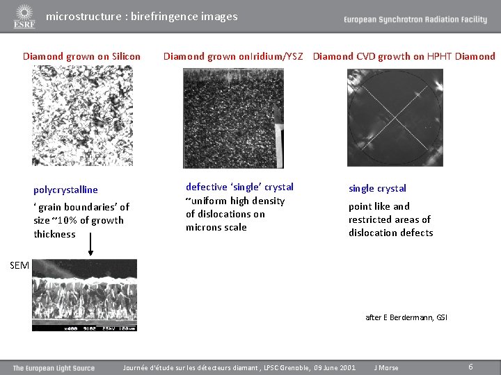
microstructure : birefringence images Diamond grown on Silicon polycrystalline ‘ grain boundaries’ of size ~10% of growth thickness Diamond grown on. Iridium/YSZ Diamond CVD growth on HPHT Diamond defective ‘single’ crystal ~uniform high density of dislocations on microns scale single crystal point like and restricted areas of dislocation defects SEM after E Berdermann, GSI Journée d'étude sur les détecteurs diamant , LPSC Grenoble, 09 June 2001 J Morse 6

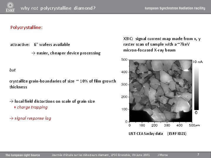
why not polycrystalline diamond? Polycrystalline: attractive: 6" wafers available → easier, cheaper device processing XBIC: signal current map made from x, y raster scan of sample with a ~7 ke. V micron-focused X-ray beam but crystallite grain-boundaries of size ~ 10% of film growth thickness → local field distortions on scale of grain size + charge trapping → signal response lag LIST-CEA Saclay data Journée d'étude sur les détecteurs diamant , LPSC Grenoble, 09 June 2001 (ESRF ID 21) J Morse 7

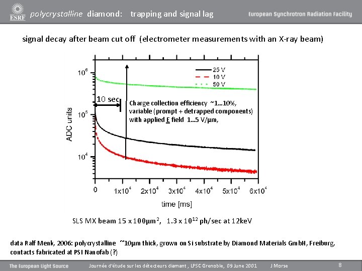
polycrystalline diamond: trapping and signal lag signal decay after beam cut off (electrometer measurements with an X-ray beam) 10 sec Charge collection efficiency ~1… 10%, variable (prompt + detrapped components) with applied E field 1… 5 V/µm, SLS MX beam 15 x 100µm 2, 1. 3 x 10¹² ph/sec at 12 ke. V data Ralf Menk, 2006: polycrystalline ~10µm thick, grown on Si substrate by Diamond Materials Gmb. H, Freiburg, contacts fabricated at PSI Nanofab (? ) Journée d'étude sur les détecteurs diamant , LPSC Grenoble, 09 June 2001 J Morse 8

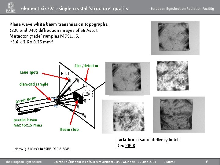
element six CVD single crystal ‘structure’ quality Plane wave white beam transmission topographs, (220 and 040) diffraction images of e 6 Ascot ‘detector grade’ samples MDS 1… 5, ~3. 6 x 0. 35 mm 3 Laue spots hkl . Film/detector diamond sample Direct beam parallel beam max 45 x 15 mm 2 Beam stop J Härtwig, F Masiello ESRF ID 19 & BM 5 variation in in same delivery batch May Dec 20052008 Journée d'étude sur les détecteurs diamant , LPSC Grenoble, 09 June 2001 J Morse 9
![e 6 CVD material bulk crystal lattice defects 1 0 0 CVD grown diamond e 6 CVD material, bulk crystal lattice defects [1, 0, 0] CVD grown diamond](https://slidetodoc.com/presentation_image_h/016a733dcdaeb70ca939a4d2d62fcec3/image-10.jpg)
e 6 CVD material, bulk crystal lattice defects [1, 0, 0] CVD grown diamond plates show clusters of threading dislocations that often result in high localized leakage currents when the metal-contacted plate is biased. optical cross polarimetry X-ray topography e 6 -DDL sample #1586 (2009) Journée d'étude sur les détecteurs diamant , LPSC Grenoble, 09 June 2001 J Morse 10

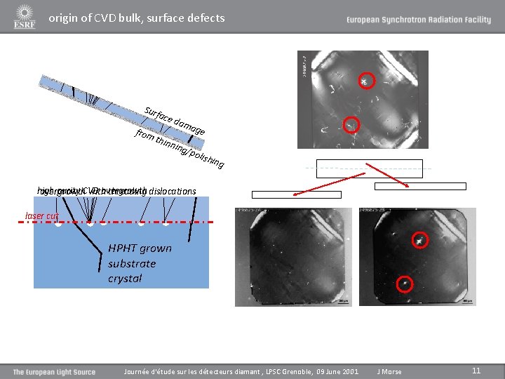
origin of CVD bulk, surface defects threading dislocations → crystal strain visible with X-ray diffraction topography or by polarized optical light transmission (birefringence) Surf from ace d ama thin ning ge /po li shin g high purity CVD overgrowth withovergrowth threading dislocations laser cut HPHT grown substrate crystal M. P. Gaukroger et al. , Diam Relat. Mat. 2008 Journée d'étude sur les détecteurs diamant , LPSC Grenoble, 09 June 2001 J Morse 11

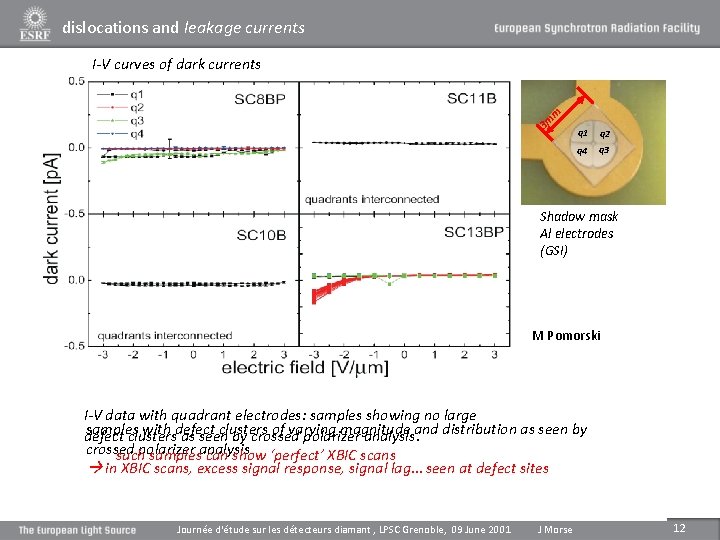
dislocations and leakage currents 3 m m I-V curves of dark currents q 1 q 2 q 4 q 3 Shadow mask Al electrodes (GSI) M Pomorski I-V data with quadrant electrodes: samples showing no large samples with defect clusters of varying magnitude defect clusters as seen by crossed polarizer analysisand. distribution as seen by crossed suchpolarizer samplesanalysis can show ‘perfect’ XBIC scans in XBIC scans, excess signal response, signal lag… seen at defect sites Journée d'étude sur les détecteurs diamant , LPSC Grenoble, 09 June 2001 J Morse 12

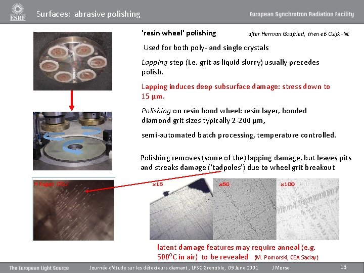
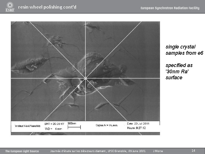
Surfaces: abrasive polishing 'resin wheel' polishing after Herman Godfried, then e 6 Cuijk -NL Used for both poly- and single crystals Lapping step (i. e. grit as liquid slurry) usually precedes polish. Lapping induces deep subsurface damage: stress down to 15 µm. Polishing on resin bond wheel: resin layer, bonded diamond grit sizes typically 2 -200 µm, semi-automated batch processing, temperature controlled. Polishing removes (some of the) lapping damage, but leaves pits and streaks damage (‘tadpoles’) due to wheel grit breakout H Kagan, OSU latent damage features may require anneal (e. g. 500ºC in air) to be revealed (M. Pomorski, CEA Saclay) Journée d'étude sur les détecteurs diamant , LPSC Grenoble, 09 June 2001 J Morse 13

resin wheel polishing cont'd Etienne Bustarret, Insitut Néel, CNRS, Grenoble single crystal samples from e 6 specified as '30 nm Ra' surface Journée d'étude sur les détecteurs diamant , LPSC Grenoble, 09 June 2001 J Morse 14

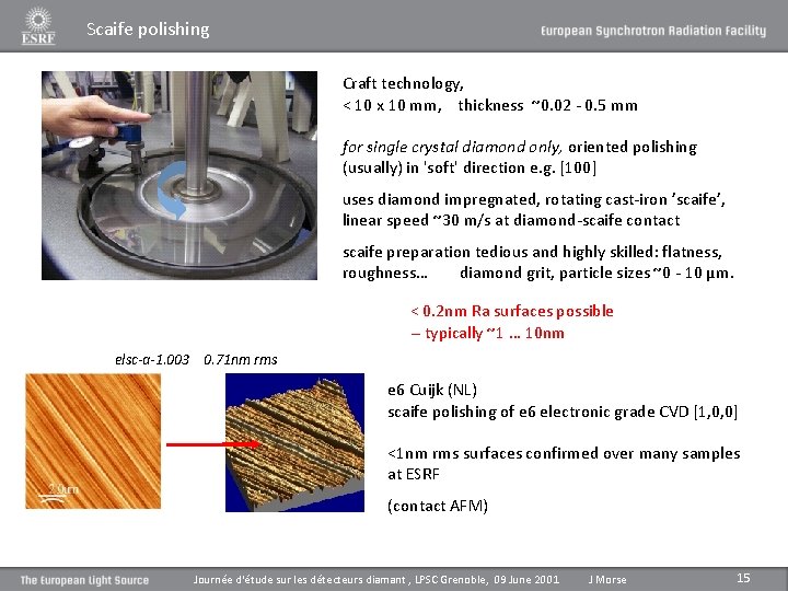
Scaife polishing Craft technology, < 10 x 10 mm, thickness ~0. 02 - 0. 5 mm for single crystal diamond only, oriented polishing (usually) in 'soft' direction e. g. [100] uses diamond impregnated, rotating cast-iron ’scaife’, linear speed ~30 m/s at diamond-scaife contact scaife preparation tedious and highly skilled: flatness, roughness… diamond grit, particle sizes ~0 - 10 µm. < 0. 2 nm Ra surfaces possible -- typically ~1 … 10 nm elsc-a-1. 003 0. 71 nm rms e 6 Cuijk (NL) scaife polishing of e 6 electronic grade CVD [1, 0, 0] <1 nm rms surfaces confirmed over many samples at ESRF (contact AFM) Journée d'étude sur les détecteurs diamant , LPSC Grenoble, 09 June 2001 J Morse 15
![scaife abrasive polishing variability e 6 sinhgle crystal CVD 100 laser breadsliced into two scaife abrasive polishing variability: e 6 sinhgle crystal CVD [100], laser ‘breadsliced’ into two](https://slidetodoc.com/presentation_image_h/016a733dcdaeb70ca939a4d2d62fcec3/image-16.jpg)
scaife abrasive polishing variability: e 6 sinhgle crystal CVD [100], laser ‘breadsliced’ into two plates, then surfaces fine scaifed by DDK-USA Same sample, factor of 7 between rms roughness of the two sides… 5 x 5 µm 2 side 1 side 2 RMS: 0. 1 nm RMS: 0. 7 nm AFM at IAF-Freiburg by Armin Kriele Journée d'étude sur les détecteurs diamant , LPSC Grenoble, 09 June 2001 J Morse 16

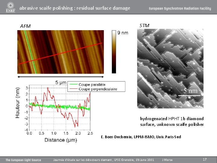
abrasive scaife polishing : residual surface damage STM AFM hydrogenated HPHT 1 b diamond surface, unknown scaife polisher E. Boer-Duchemin, LPPM-ISMO, Univ. Paris-Sud Journée d'étude sur les détecteurs diamant , LPSC Grenoble, 09 June 2001 J Morse 17

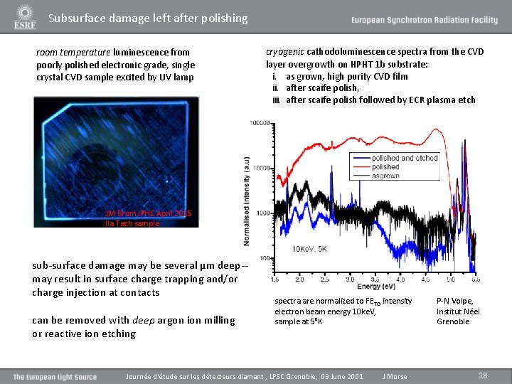
Subsurface damage left after polishing cryogenic cathodoluminescence spectra from the CVD layer overgrowth on HPHT 1 b substrate: i. as grown, high purity CVD film ii. after scaife polish, iii. after scaife polish followed by ECR plasma etch room temperature luminescence from poorly polished electronic grade, single crystal CVD sample excited by UV lamp H Kagan OSU JM Brom IPHC April 2015 IIa Tech sample sub-surface damage may be several µm deep-may result in surface charge trapping and/or charge injection at contacts can be removed with deep argon ion milling or reactive ion etching spectra are normalized to FETO intensity electron beam energy 10 ke. V, sample at 5°K Journée d'étude sur les détecteurs diamant , LPSC Grenoble, 09 June 2001 J Morse P-N Volpe, Institut Néel Grenoble 18

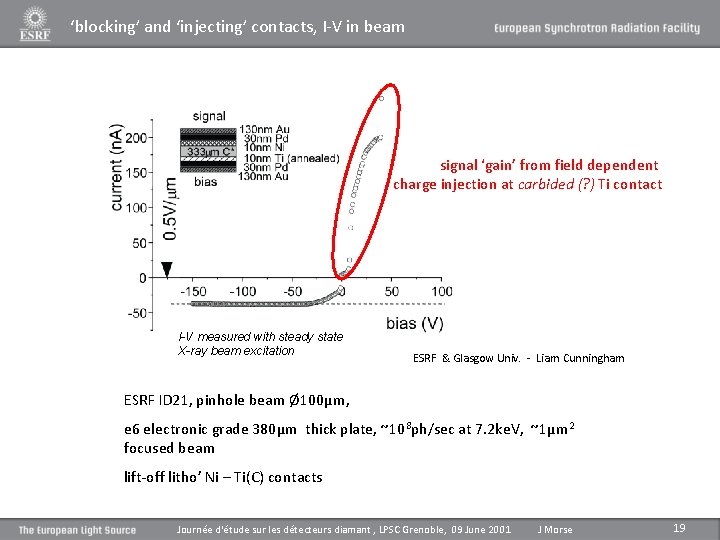
‘blocking’ and ‘injecting’ contacts, I-V in beam signal ‘gain’ from field dependent charge injection at carbided (? ) Ti contact I-V measured with steady state X-ray beam excitation ESRF & Glasgow Univ. - Liam Cunningham ESRF ID 21, pinhole beam Ø 100µm, e 6 electronic grade 380µm thick plate, ~108 ph/sec at 7. 2 ke. V, ~1µm 2 focused beam lift-off litho’ Ni – Ti(C) contacts Journée d'étude sur les détecteurs diamant , LPSC Grenoble, 09 June 2001 J Morse 19

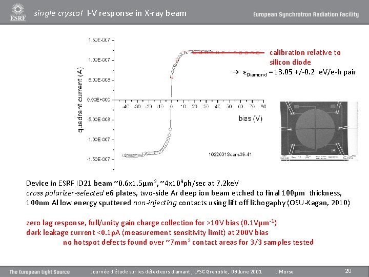
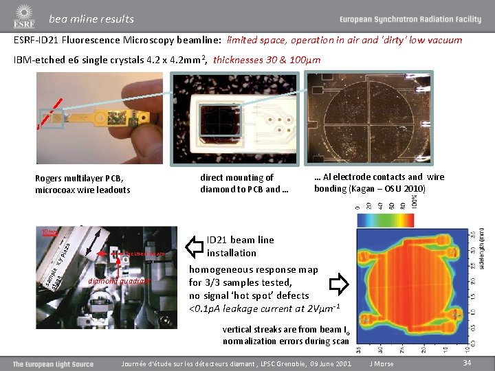
single crystal I-V response in X-ray beam calibration relative to silicon diode → εDiamond = 13. 05 +/-0. 2 e. V/e-h pair Device in ESRF ID 21 beam ~0. 6 x 1. 5µm 2, ~4 x 10⁹ ph/sec at 7. 2 ke. V cross polarizer-selected e 6 plates, two-side Ar deep ion beam etched to final 100µm thickness, 100 nm Al low energy sputtered non-injecting contacts using lift off lithogaphy (OSU-Kagan, 2010) zero lag response, full/unity gain charge collection for >10 V bias (0. 1 Vµm -1) dark leakage current <0. 1 p. A (measurement sensitivity limit) at 200 V bias no hotspot defects found over ~7 mm 2 contact areas for 3/3 samples tested Journée d'étude sur les détecteurs diamant , LPSC Grenoble, 09 June 2001 J Morse 20

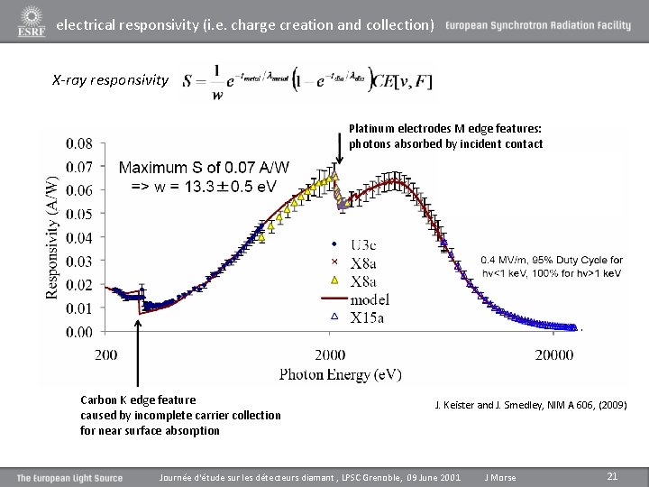
electrical responsivity (i. e. charge creation and collection) X-ray responsivity Platinum electrodes M edge features: photons absorbed by incident contact Carbon K edge feature caused by incomplete carrier collection for near surface absorption J. Keister and J. Smedley, NIM A 606, (2009) Journée d'étude sur les détecteurs diamant , LPSC Grenoble, 09 June 2001 J Morse 21

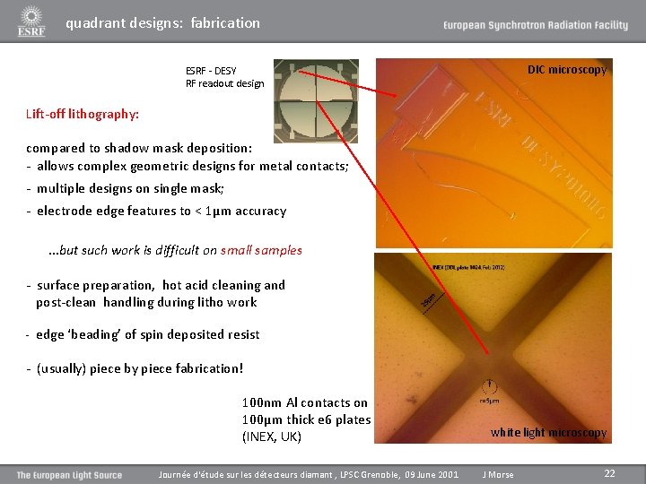
quadrant designs: fabrication DIC microscopy ESRF - DESY RF readout design Lift-off lithography: compared to shadow mask deposition: - allows complex geometric designs for metal contacts; - multiple designs on single mask; - electrode edge features to < 1µm accuracy …but such work is difficult on small samples - surface preparation, hot acid cleaning and post-clean handling during litho work - edge ‘beading’ of spin deposited resist - (usually) piece by piece fabrication! 100 nm Al contacts on 100µm thick e 6 plates (INEX, UK) Journée d'étude sur les détecteurs diamant , LPSC Grenoble, 09 June 2001 white light microscopy J Morse 22

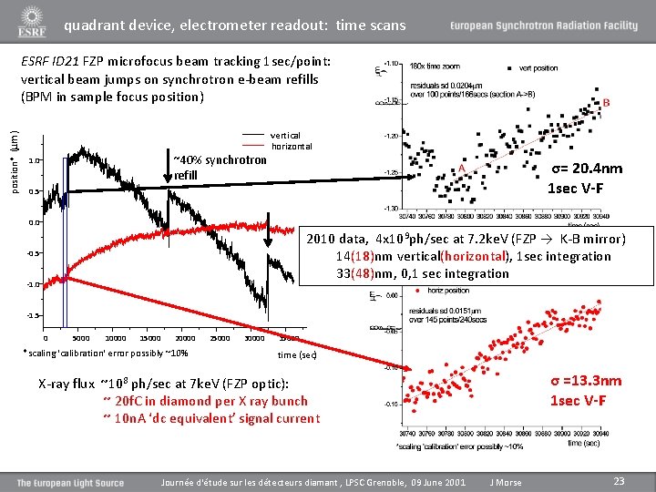
quadrant device, electrometer readout: time scans position* (µm ) ESRF ID 21 FZP microfocus beam tracking 1 sec/point: vertical beam jumps on synchrotron e-beam refills (BPM in sample focus position) ~40% synchrotron refill 1. 0 vertical horizontal σ= 20. 4 nm 1 sec V-F 0. 5 0. 0 2010 data, 4 x 10⁹ ph/sec at 7. 2 ke. V (FZP → K-B mirror) 14(18)nm vertical(horizontal), 1 sec integration 33(48)nm, 0, 1 sec integration -0. 5 -1. 0 -1. 5 0 5000 10000 15000 20000 *scaling 'calibration' error possibly ~10% 25000 30000 35000 time (sec) σ =13. 3 nm 1 sec V-F X-ray flux ~108 ph/sec at 7 ke. V (FZP optic): ~ 20 f. C in diamond per X ray bunch ~ 10 n. A ‘dc equivalent’ signal current Journée d'étude sur les détecteurs diamant , LPSC Grenoble, 09 June 2001 J Morse 23

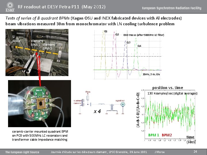
RF readout at DESY Petra P 11 (May 2012) Tests of series of 8 quadrant BPMs (Kagan OSU and INEX fabricated devices with Al electrodes) beam vibrations measured 30 m from monochromator with LN cooling turbulence problem Q 1 Si diode diamond BPM-1 diamond BPM-2 Q 2 DSO traces (after 500 MHz LC filter) Q 3 Q 4 20 m. V, 5 ns /div (A+B-C-D)/(A+B+C+D) x 4 position vs. time ceramic-carrier mounted quadrant BPM on PCB with 500 MHz LC resonators and transformer cable impedance matching Journée d'étude sur les détecteurs diamant , LPSC Grenoble, 09 June 2001 130 ksamples/sec (digital averages) BPM 1 BPM 2 J Morse time (secs) 24

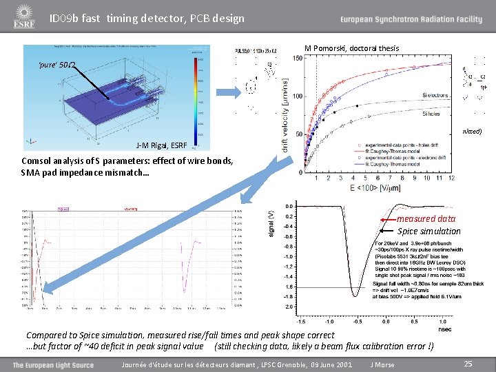
ID 09 b fast timing detector, PCB design M Pomorski, doctoral thesis 'pure' 50 W (contribution of Picosec Labs PSPL 5531 bias tee omitted) J-M Rigal, ESRF Comsol analysis of S parameters: effect of wire bonds, SMA pad impedance mismatch… measured data Spice simulation signal at SMA connector signal at DSO diamond current pulse Compared to Spice simulation, measured rise/fall times and peak shape correct …but factor of ~40 deficit in peak signal value (still checking data, likely a beam flux calibration error !) Journée d'étude sur les détecteurs diamant , LPSC Grenoble, 09 June 2001 J Morse 25

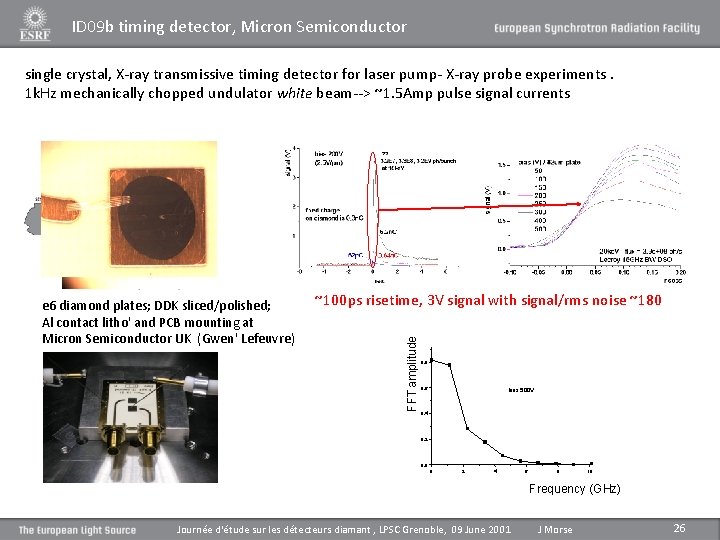
ID 09 b timing detector, Micron Semiconductor single crystal, X-ray transmissive timing detector for laser pump- X-ray probe experiments. 1 k. Hz mechanically chopped undulator white beam--> ~1. 5 Amp pulse signal currents ~100 ps risetime, 3 V signal with signal/rms noise ~180 FFT amplitude e 6 diamond plates; DDK sliced/polished; Al contact litho' and PCB mounting at Micron Semiconductor UK (Gwen' Lefeuvre) 0. 8 0. 6 bias 500 V 0. 4 0. 2 0. 0 0 2 4 6 8 10 Frequency (GHz) Journée d'étude sur les détecteurs diamant , LPSC Grenoble, 09 June 2001 J Morse 26

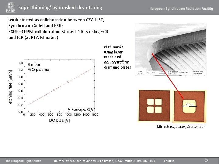
'Superthinning' by masked dry etching work started as collaboration between CEA-LIST, Synchrotron Soleil and ESRF –CRPM collaboration started 2015 using ECR and ICP (at PTA-Minatec) etch masks using laser machined polycrystalline diamond plates 2 mm M Pomorski, CEA Micro. Usinage. Laser, Grattentour Journée d'étude sur les détecteurs diamant , LPSC Grenoble, 09 June 2001 J Morse 27

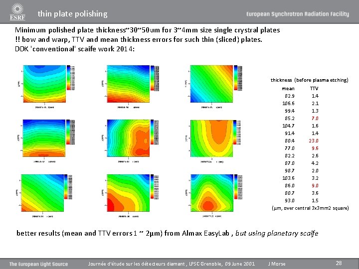
thin plate polishing Minimum polished plate thickness~30~50 um for 3~4 mm size single crystral plates !! bow and warp, TTV and mean thickness errors for such thin (sliced) plates. DDK 'conventional' scaife work 2014: thickness (before plasma etching) mean TTV 82. 9 1. 4 106. 6 2. 1 99. 4 1. 3 85. 2 7. 0 104. 7 1. 6 91. 4 80. 4 23. 0 77. 0 9. 6 82. 2 2. 6 87. 0 4. 2 98. 7 2. 0 103. 6 3. 2 86. 0 9. 0 80. 7 3. 6 93. 0 1. 5 (µm, over central 3 x 3 mm 2 square) better results (mean and TTV errors 1 ~ 2µm) from Almax Easy. Lab , but using planetary scaife Journée d'étude sur les détecteurs diamant , LPSC Grenoble, 09 June 2001 J Morse 28

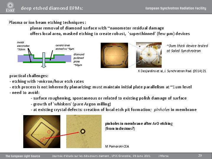
deep etched diamond BPMs: Plasma or ion beam etching techniques : planar removal of diamond surface with ~nanometer residual damage offers local area, masked etching to create robust, 'superthinned' (few µm) devices metal electrodes ~50 nm ~3 um thick device tested at Soleil Synchrotron central area etched to ~3µm diamond polished plate ~50µm K Desjardins et al, J. Synchrotron Rad. (2014) 21 practical challenges: - etching with >micron/hour etch rates - etch process is not inherently planarizing: must maintain initial plate parallelism at ~1 um level - need to avoid: - surface roughening, spontaneous or related to existing polish damage of surface - growth of 'whiskers' (pure Argon milling) - at existing crystal defects: creation of local etch pit formation; pinholes in membrane after Ar. O etching (from inclusions? ) M Pomorski-CEA Journée d'étude sur les détecteurs diamant , LPSC Grenoble, 09 June 2001 J Morse 29

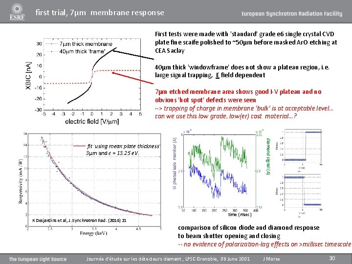
first trial, 7µm membrane response First tests were made with 'standard' grade e 6 single crystal CVD plate fine scaife polished to ~50µm before masked Ar. O etching at CEA Saclay 40µm thick 'windowframe' does not show a plateau region, i. e. large signal trapping, E field dependent K Desjardins et al, J. Synchrotron Rad. (2014) 21 diamond signal (A) fit using mean plate thickness 3µm and ε = 13. 25 e. V. Si photodiode monitor (A) 7µm etched membrane area shows good I-V plateau and no obvious 'hot spot' defects were seen --> trapping of charge in membrane 'bulk' is at acceptable level… can we use this low grade, low(er) cost material…? time (msec) comparison of silicon diode and diamond response to beam shutter opening and closing -- no evidence of polarization-lag effects on >millisec timescale Journée d'étude sur les détecteurs diamant , LPSC Grenoble, 09 June 2001 J Morse 30

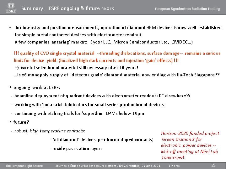
Summary , ESRF ongoing & future work • for intensity and position measurements, operation of diamond BPM devices is now well established for simple metal contacted devices with electrometer readout, a few companies ‘entering’ market: Sydor LLC, Micron Semiconductor Ltd, CIVIDEC…) !!! quality of CVD single crystal material --threading dislocations, surface damage-- remains a serious limit for device yield (localized high dark currents and injection ‘gain’ effects) !!! → careful selection of material still necessary after 10 years! …is e 6 monopoly supply of ‘detector grade’ diamond material now ending with IIa-Tech Singapore? ? • ongoing work at ESRF: - beamline deployment of quadrant devices with electrometer readout (RF elsewhere? ) - working with 'industrial' fabricators for small series production of devices - continuing with etching trials for 'superthin' BPMs below 10µm • future? - robust, high temperature contacts: - 'all diamond' devices (p++ boron-doped contacts) - oxide passivation layers Journée d'étude sur les détecteurs diamant , LPSC Grenoble, 09 June 2001 Horizon-2020 funded project 'Green Diamond' for electronic power devices -kick-off meeting at Néel Lab tomorrow! J Morse 31

Thank-you for your attention Journée d'étude sur les détecteurs diamant , LPSC Grenoble, 09 June 2001 J Morse 32

Journée d'étude sur les détecteurs diamant , LPSC Grenoble, 09 June 2001 J Morse 33

bea mline results ESRF-ID 21 Fluorescence Microscopy beamline: limited space, operation in air and 'dirty' low vacuum IBM-etched e 6 single crystals 4. 2 x 4. 2 mm 2, thicknesses 30 & 100µm sam sta ple ge x, y tag pie o szo can s 10 mm direct mounting of diamond to PCB and … … Al electrode contacts and wire bonding (Kagan – OSU 2010) e Rogers multilayer PCB, microcoax wire leadouts focused beam diamond quadrant ID 21 beam line installation homogeneous response map for 3/3 samples tested, no signal ‘hot spot’ defects <0. 1 p. A leakage current at 2 Vµm-1 vertical streaks are from beam Io normalization errors during scan Journée d'étude sur les détecteurs diamant , LPSC Grenoble, 09 June 2001 J Morse 34
![e 6 CVD sample variability polarized light transmission parallel to 100 350µm thick plates e 6 CVD sample variability polarized light transmission parallel to [100], 350µm thick plates](https://slidetodoc.com/presentation_image_h/016a733dcdaeb70ca939a4d2d62fcec3/image-35.jpg)
e 6 CVD sample variability polarized light transmission parallel to [100], 350µm thick plates screening of 25 samples at ESRF Δn 4 x 10 -5 8 x 10 -5 white is ‘over scale’ Journée d'étude sur les détecteurs diamant , LPSC Grenoble, 09 June 2001 J Morse 35

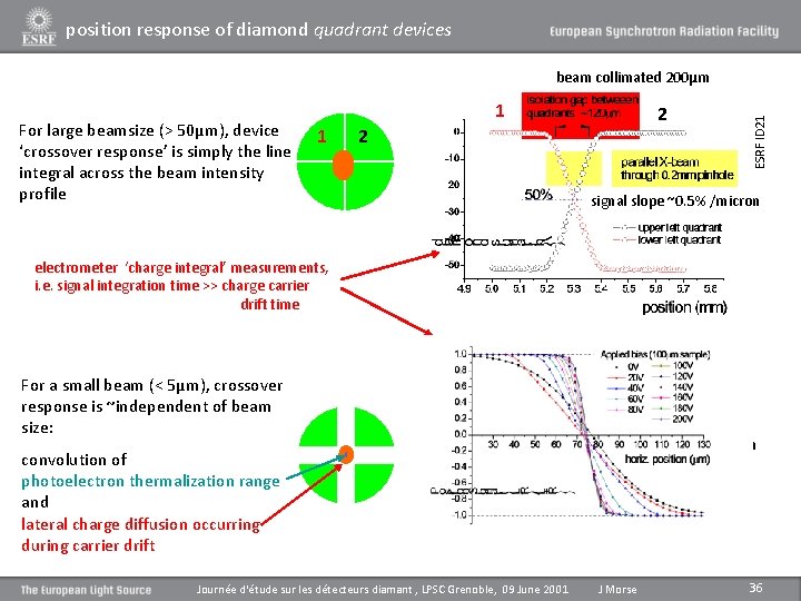
position response of diamond quadrant devices For large beamsize (> 50µm), device ‘crossover response’ is simply the line integral across the beam intensity profile 1 1 Line scan @ 7. 2 ke. V 2 2 ESRF ID 21 beam collimated 200µm signal slope ~0. 5% /micron electrometer ‘charge integral’ measurements, i. e. signal integration time >> charge carrier drift time isolation gap ~120µm For a small beam (< 5µm), crossover response is ~independent of beam size: convolution of photoelectron thermalization range and lateral charge diffusion occurring during carrier drift Journée d'étude sur les détecteurs diamant , LPSC Grenoble, 09 June 2001 signal slope ~5% /micron …beam focused <1µm J Morse 36

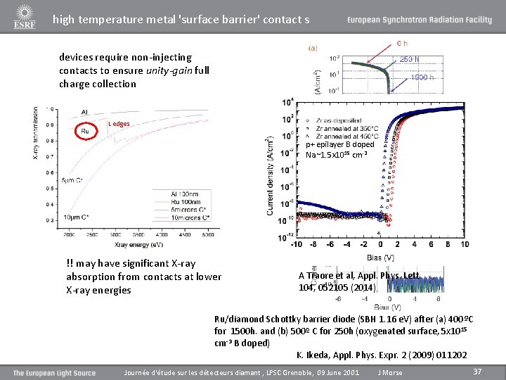
high temperature metal 'surface barrier' contact s devices require non-injecting contacts to ensure unity-gain full charge collection L edges p+ epilayer B doped Na ~1. 5 x 1015 cm-3 !! may have significant X-ray absorption from contacts at lower X-ray energies A Traore et al, Appl. Phys. Lett. 104, 052105 (2014) Ru/diamond Schottky barrier diode (SBH 1. 16 e. V) after (a) 400ºC for 1500 h. and (b) 500º C for 250 h (oxygenated surface, 5 x 1015 cm-3 B doped) K. Ikeda, Appl. Phys. Expr. 2 (2009) 011202 Journée d'étude sur les détecteurs diamant , LPSC Grenoble, 09 June 2001 J Morse 37