Thin Film Technology HANYANG UNIVERSITY HANYANG UNIVERSITY Introduction
 한양대학교 HANYANG UNIVERSITY 신소재공학과 전형탁 한양대학교 HANYANG UNIVERSITY")


 Polycrystalline (Polysilicon)")


 한양대학교 HANYANG UNIVERSITY")


 STM image of Si")


 Si(s) + 2 H 2(g) Si.")


- Slides: 56
박막공정 기술 (Thin Film Technology) 한양대학교 HANYANG UNIVERSITY 신소재공학과 전형탁 한양대학교 HANYANG UNIVERSITY
Introduction 한양대학교 HANYANG UNIVERSITY
1 Introduction 반도체 소자 제작에 많이 사용되는 박막은 열적 성장이나 물리적 증착, 혹은 반응에 의해 증착(deposition)되는 금속, 반도체 , 부도체의 얇은 층을 말함. Thin Film • Films with a thickness less than 1㎛, Films thicker than 100 ㎛ are called thick films • The basis enables modern electronic and magnetic industries. VLSI 공정용 박막은 구성 성분과 두께 등이 submicron 공정에 적합하도록 조절될 수 있어야 하고 pinhole과 같은 결합이 없어야 함. 박막 제조의 대표적인 2가지 방법 (1) 화학 기상증착(CVD : chemical vapor deposition) (2) 물리 기상증착(PVD : physical vapor deposition) 한양대학교 HANYANG UNIVERSITY
1 Introduction Thin Film Deposition Chemical Process Physical Process Plating Sol-Gel CVD Evaporation Sputtering Electroplating Dipping MOCVD Ion plating RF Electroless Spraying PECVD Laser ablation DC Spin coating ALD MBE Magnetron Electro beam 한양대학교 HANYANG UNIVERSITY
1 Introduction There are many applications for CVD ! 한양대학교 HANYANG UNIVERSITY
CVD process 한양대학교 HANYANG UNIVERSITY
2 CVD process Advantage of CVD process Low temperature process Control of the impurity concentration and distribution A wide range in thickness Near equilibrium process Choice of reactants species Large scale, multi wafer process In-situ etching of the substrates Disadvantage of CVD process Numerous control variable Use many flammable, corrosive, and toxic gases Complex system High substrate temperature 한양대학교 HANYANG UNIVERSITY
CVD process 2 CVD process Conventional CVD surface reaction Main Flow of Reactants Gases 5. 1. 2. 한양대학교 HANYANG UNIVERSITY 3. 4. 1. Diffusion-in of reactants through boundary layer 2. Adsorption of reactants on the substrate 3. Chemical reaction takes place 4. Desorption of absorbed species 5. Diffusion out of by-products
2 CVD process CVD REACTIONS AND PROCESSES TYPES OF CVD PROCESSES 1. 2. 3. 4. 5. 한양대학교 HANYANG UNIVERSITY Low Pressure (LPCVD) Plasma Enhanced (PECVD) Atmospheric Pressure (APCVD) Rapid Thermal (RTCVD) Other Atomic Layer Deposition (ALD) Photon Assisted (PCVD) Metallorganic Organic (MOCVD) Chemical Beam Epitaxy (CBE)
2 CVD process MATERIALS DEPOSITED BY CVD • SILICON Single Crystal (Epitaxy) Polycrystalline (Polysilicon) Amorphous Silicon • INSULATORS Si. O 2, Si 3 N 4, Si. Ox. Ny , Ta 2 O 5, Ti. O 2 • CONDUCTORS Metals: W, Al, Mo, Cu Silicides: Ti. Si 2, WSi 2, Ta. Si 2, Mo. Si 2 Barriers: Ti. N • OTHER MATERIALS Diamond, Si. C, Ga. N, III-V, II-VI 한양대학교 HANYANG UNIVERSITY
2 CVD process MATERIALS DEPOSITED BY CVD and ALD DRAM Structure 한양대학교 HANYANG UNIVERSITY
2 CVD process COMPARISON OF CVD TO OTHER FILM FORMATION TECHNIQUES CVD THERMAL OXIDATION EVAPORATION Physical Vapor Deposition (PVD) 한양대학교 HANYANG UNIVERSITY
2 CVD process CVD REACTORS Atmospheric Pressure, Cold-Wall System (for Epi) 한양대학교 HANYANG UNIVERSITY Low Pressure, Hot-Wall System (for Oxide, Nitride, Poly- or Amorphous- Si) From Plummer, Deal & Griffin, Fig 9 -4, p 513
2 CVD process TEMPERATURE DEPENDENCE OF SILICON GROWTH RATE Mass Transport Reaction Rate 한양대학교 HANYANG UNIVERSITY
2 CVD process FILM GROWTH STEPS We Have Looked at Details of Film Growth Reactions What is the Overall Picture of Film Growth Like? Consider the Following Steps: • Nucleation • Nuclei Growth • Coalescence • Film Formation & Secondary Nucleation 한양대학교 HANYANG UNIVERSITY
General concept 한양대학교 HANYANG UNIVERSITY
3 General concept Thin film growth mode ◆Benjamin Franklin’s story 큰 연못을 보았고 표면이 매우 rough 한 것을 관찰 함. →연못에 a spoonful of oil 뿌리면 pond became very smooth →Forms a film about 1 nm thickness on the pond →A film only a few nm thick wets a surface and dramatically changes its surface properties ◆SE is defined as the energy spent to create a surface Positive(+) quantity Liquid → tends to ball up to reduce its surface area Crystal → tends to facet to expose those surfaces of lowest energy SE → related to bond E and to number of broken bonds Related to the binding E of the material 한양대학교 HANYANG UNIVERSITY
3 General concept Thin film growth mode ◆Thin film growth modes Thermodynamic Theory Assumptions No chemical reactions No alloying No interdiffusion No other changes at the interface Substrate σs= σi+σ0 cosθ 1) θ>0 island growth (Volmer-Weber) σs<σ0+σi 2) θ=0 layer growth (Frank-van der Merwe) σs≥σo+σi Strain Energy가 overgrowth에서 σ0 보다 작을 때 3) θ=0 Stranski-Krastanov σs≥σ0+σi 한양대학교 HANYANG UNIVERSITY Strain Energy가 overgrowth에서 σ0 보다 클 때
3 General concept Thin film growth mode Three different mechanisms 1. The layer-by-layer growth (Frank-van der Merwe mechanism) 2. A three dimensional nucleation, forming and growth and coalescence of islands (Volmer- Weber mechanism) 3. Adsorption of a monolayer and subsequent nucleation on the top of this layer (Stranski- Krastanov mechanism) 1. Island (Volmer-Weber) Growth Mode - Atoms in the film are more strongly bound to each other than to the substrate - metal and semiconductor film deposited on oxide 2. Layer (Frank – van der Merwe) Growth Mode Atoms are more strongly bound to the substrate than to each other layer by layer growth 3. Layer + Island ( Stranski - Krastanov) Growth Mode Intermediate (1) & (2) strain energy due to lattice mismatch trigger island formation metal / metal, metal / semiconductor 한양대학교 HANYANG UNIVERSITY -
3 General concept Thin film growth mode Fig 7 -2 Basic modes of thin-film growth. 한양대학교 HANYANG UNIVERSITY
3 General concept Thin film growth mode CAPILLARITY THEORY OF HETEROGENEOUSE NUCLEATION Capillarity theory possesses the mixed virtue of yielding a conceptually simple qualitative model of film nucleation which is however quantitatively inaccurate The lack of detailed atomistic assumptions gives theory an attractive broad generality with the power of creating useful connections among such variables as substrate temperature deposition rate, and critical film nucleus size DEPOSITION fv sv VAPOR fs FILM a 0 NUCLEUS r 한양대학교 HANYANG UNIVERSITY DESORPTION SUBSTRATE Fig. 7 -11 Schematic of basic atomistic nucleation processes on substrate surface during vapor deposition
3 General concept Thin film growth mode a 3 r 3 = ( 2 - 3 cos + cos 3 ) / 3 r 3 : volume a 2 r 2 = sin 2 r 2 : projected circular area a 1 r 2 = 2 ( 1 - cos ) r 2 : curved surface area Young’s equation: mechanical equilibrium among the interfacial tensions sv = fs + vf cos or cos = ( sv - fs) / fv island growth : > 0 sv < fs + vf layer growth : = 0 sv = fs + vf If fs = 0 (no interface ) homo- or autoepitaxy S. K growth : sv > fs + vf The strain energy of film overgrowth is large with respect to vf , permitting nuclei to form above the layer 한양대학교 HANYANG UNIVERSITY
3 General concept Thin film growth mode The critical nucleus size r* Both r* & ∆ G* scale in manner showing An aggregate smaller in size than r* disappears by shrinking , lowering ∆ G in the process G* : energy barrier to the nucleus process If r < r* : cluster is unstable and shrink r > r* : cluster is stable and grow larger while lowering the energy of system 한양대학교 HANYANG UNIVERSITY
3 General concept Thin film growth mode In heterogeneous nucleation the accommodating substrate catalyzes vapor condensation by lowering the energy barrier ∆ G* through a reduction of the contact angle First term: Homogeneous nucleation Second term: geometric constant Wetting(layer) : wetting factor = 0 at = 0 Dewetting(sphere) : w. f. =1, at = 180 film wets the substrate no barrier to nucleation dewetting ∆ G* is maximum and equal to that for homogeneous nucleation ∆ G* is its strong influence on the density (N*) of stable nuclei that can be expected to survive N* = ns exp - ∆ G* / k. BT 한양대학교 HANYANG UNIVERSITY ns : total nucleation site density
3 General concept Thin film growth mode FILM GROWTH MODES Young’s equation sv = fs + fv cos or cos = ( sv - fs )/ fv Island growth, >0 sv < fs + fv In the case of Layer growth the deposit “wets” the substrate and 0 sv ≥ fs + fv A special case of this condition is ideal homo- or auto-epitaxy interface between film and substrate essentially vanishes, fs = 0 In general materials with low surface energy will wet substrate with a higher surface energy S-K growth sv > fs + fv In this case the strain energy per unit area of the film overgrowth is large with respect to fv permitting nuclei to from above the initial layer 한양대학교 HANYANG UNIVERSITY
3 General concept Thin film growth mode Si on Si(001) STM image of Si deposition on three successive terraces Arrhenius plot of island density vs the reciprocal of the substrate temperature Si on Si(001) the new layer of adatom islands form dimer rows ( formation of adatoms and ad-dimers) Anisotropic diffusion of Si adatoms At 500 K, adatom transport is 1000 times faster in direction parallel to dimer rows than perpendicular to them 한양대학교 HANYANG UNIVERSITY
3 General concept Thin film growth mode Metals on Si In the case of Ag Only 1/3 of a monolayer deposits on this surface at 90℃ Individual adatoms of Ag Larger faceted clusters ( additional Ag atoms attach to the initial nuclei ) STM image - Ag nuclei on (111) Si 한양대학교 HANYANG UNIVERSITY
3 General concept Thin film growth mode VARIOUS STAGES OF FILM GROWTH 한양대학교 HANYANG UNIVERSITY
3 General concept Thin film growth mode Vapor Pressure Above a Cluster ◆Cluster grows in 2 ways ripening coalescence Ripening Process : mass transport from smaller cluster to larger cluster by atomic surface diffusion Larger cluster grows gradually at the expense of smaller clusters. Flux of atoms from the cluster depend on the cluster size. Driving force : Concentration gradient Coalescence : simply whole clusters coming together two clusters combine to form a single large clusters larger cluster represents a lower energy state than two separate clusters Driving force : surface energy reduction 한양대학교 HANYANG UNIVERSITY
3 General concept Thin film growth mode Vapor Pressure Above a Cluster Driving force for ripening Concentration gradient of material associated with the difference in vapor pressure over different size clusters. Vapor Pressure of Small Clusters > Vapor Pressure of Large Clusters →Atoms move to large cluster across the surface to attach themselves to a large cluster →Smaller cluster shrinks and the large cluster grows as a function of time 한양대학교 HANYANG UNIVERSITY
3 General concept Thin film growth mode Vapor Pressure Above a Cluster ◆The existence of Ga clusters on Ga. As → See Fig 5. 3 한양대학교 HANYANG UNIVERSITY
3 General concept Thin film growth mode Coalescence ◆Coalescence → Combine two clusters into a larger cluster ◆Compare the total surface Energy of two clusters to that of one cluster Total Surface Energy of Two Clusters (R 1 : radius) Combined cluster has a same total volume of individual cluster 한양대학교 HANYANG UNIVERSITY
3 General concept Thin film growth mode Coalescence Total volume of a large cluster Total surface Energy of a single large cluster Ratio of total E => New surface area is less than the total surface area of the two smaller clusters and there is thus less total surface energy 한양대학교 HANYANG UNIVERSITY
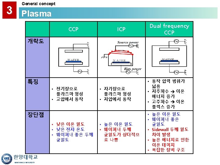
3 General concept Plasma • A Gas Discharge is Created by Electromagnetic Energy: - RF (radio frequency) - Microwave (ECR) • Reactive Species are Created by the Plasma Discharge Lower Temperature Deposition (<400°C) • Large Amounts of H are Frequently Found in Plasma CVD Films. • Primary Applications: - Interlayer Dielectrics - Passivation Layer Over Low Temp. Material (i. e. Al) 한양대학교 HANYANG UNIVERSITY
3 General concept Plasma 한양대학교 HANYANG UNIVERSITY
3 General concept Plasma 한양대학교 HANYANG UNIVERSITY
3 General concept Plasma 한양대학교 HANYANG UNIVERSITY
3 General concept Plasma 한양대학교 HANYANG UNIVERSITY
3 General concept Plasma 한양대학교 HANYANG UNIVERSITY
3 General concept Plasma 한양대학교 HANYANG UNIVERSITY
3 General concept CVD system HOT WALL PRACTICAL CVD SYSTEM CONSIDERATIONS • Uniform Temperature Distribution Better Film Uniformity • Sidewall Deposition Source of Particulates Use Soft-Landing Cantilever Loading Depletes Active Species Requires Offsetting Temperature Gradient (which may produce gradient in Poly-Si grain sizes) "Memory" Effects - May Require Conditioning Can Block Lamp Irradiation • Ready Availability of Horizontal and Vertical Furnaces COLD WALL • No Deposition on Walls Fewer Particulates, Less Memory Effects • Facilitates Use of RTP and Integration into Clusters 한양대학교 HANYANG UNIVERSITY
3 General concept CVD system • Hot Wall Reactors Have Been the Primary Choice 한양대학교 HANYANG UNIVERSITY
3 General concept CVD system LOW PRESSURE • Reaction-Limited Regime Requires Good Temperature Control and Uniformity ATMOSPHERIC (HIGH) PRESSURE • Transport-Limited Regime Requires Good Flow Control to get Uniform Films • Gas-Phase Nucleation Generates Particulates Dilute Active Species with Nitrogen 한양대학교 HANYANG UNIVERSITY
3 General concept CVD system HORIZONTAL TUBE • Wafer-to-Wafer Spacing Depends on Width of Slots and Tilting • Lower Cost ~ 5% Uniformity of Poly-Si VERTICAL TUBE • Wafer-to-wafer Spacing is More Uniform (Wafers Held By Gravity) • Convective Effects are More Evenly Distributed Across Wafer • Reduced Particle Counts • Easier robotic Handling of Large Wafers • Smaller Footprint in Fab ~ 2% Uniformity of Undoped Poly-Si and Nitride 한양대학교 HANYANG UNIVERSITY
3 General concept CVD system • Load Boats • Seal O-ring Door • Flush with Inert Gas (Nitrogen) • Pump Down • Ramp up Temperature • Turn on CVD Gases and Deposit Film • Turn off Gases and Flush with Inert Gas • Ramp Down Temperature • Pull Boat Out 한양대학교 HANYANG UNIVERSITY
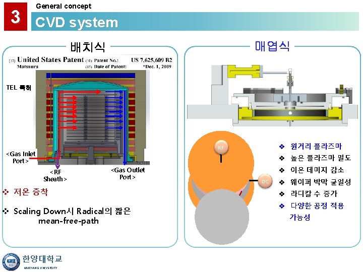
3 General concept CVD system Direct Remote HF CCP type LF ICP type 다중 plasma 구조 CCP와 ICP 적용 가능 Remote type 대부분의 Dual frequency plasma 구조 한양대학교 HANYANG UNIVERSITY or DC
3 General concept CVD system 한양대학교 HANYANG UNIVERSITY
3 General concept CVD system 한양대학교 HANYANG UNIVERSITY
3 General concept Si deposition We Have Considered the Generic CVD Process. Let's Examine Some Examples in Detail Consider First a Very Important Material: SILICON Deposition of Silicon Can be Grouped Into Three Types, Depending on the Film Structure. 1. Single Crystal (Epitaxial) 2. Polycrystalline (Polysilicon) 3. Amorphous 한양대학교 HANYANG UNIVERSITY
3 General concept Si epitaxial deposition With the Appropriate Choice of Reactor, Gas Chemistry, and Process Variables, Single Crystal Si Can be Deposited as a Continuation of the Underlying Lattice EPITAXY: Growth of a Thin Crystalline Layer on a Crystalline Substrate Consider Some Typical Chemical Reactions Used for Epitaxial Silicon Deposition 한양대학교 HANYANG UNIVERSITY
3 General concept Si deposition Si. H 4(g) Si(s) + 2 H 2(g) Si. H 2 Cl 2(g) Si(s) + H 2(g) + Cl 2(g) Si. HCl 3(g) Si(s) + HCl(g) + Cl 2(g) Si. Cl 4(g) Si(s) + 2 Cl 2(g) Si 2 H 6(g) Si(s) + 3 H 2(g) H 2 is often added to the above as in: Si. Cl 4(g) + 2 H 2(g) Si(s) + 4 HCl (g) Properties of Films and the Required Process Variables Vary From Reaction to Reaction 한양대학교 HANYANG UNIVERSITY
3 General concept Si deposition q Step Coverage : 2020 -11 -29 한양대학교 HANYANG UNIVERSITY Film Deposition
3 General concept Si deposition DRAM Cell Structure 한양대학교 HANYANG UNIVERSITY
General concept 3 Si deposition Ø CVD for silicon Epitaxial Growth Techniques • 4개의 silicon source 가 VPE 성장을 위해 사용된다. : silicon tetrachloride (Si. Cl 4), dichlorosilane (Si. H 2 Cl 2), trichlorosilane (Si. HCl 3), silane (Si. H 4) • 일반적 반응온도는 1200℃ 이고, 다른 silicon source 들은 더 낮은 반응온도 때문에 사용되어진다. Silicon-tetrachloride 로부터 각 염소 원자에 대한 수소 원자의 치환은 반응 온도에서 약 50℃ 정도의 감소를 가능케 한다. • Silicon tetrachloride 의 전체적인 반응은 Si. Cl 4 (gas) + 2 H 2 (gas) • Si (solid) + 4 HCl (gas) 추가적인 경쟁적 반응은 주어진 식 1을 따라 일어난다. Si. Cl 4 (gas) + Si (solid) 2 Si. Cl 2 (gas) (1) (2) 결과적으로 silicon tetrachloride 의 농도가 매우 높다면 silicon 의 성장보다는 etching이 일어날 것이다. 한양대학교 HANYANG UNIVERSITY