These slides incorporate figures from Digital Design Principles
- Slides: 32

These slides incorporate figures from Digital Design Principles and Practices, third edition, by John F. Wakerly, Copyright 2000, and are used by permission. NO permission is given to re-use or publish these figures, in either original or modified form, in printed, electronic or any other format. 1

Slide Set 13 Random access memory 2

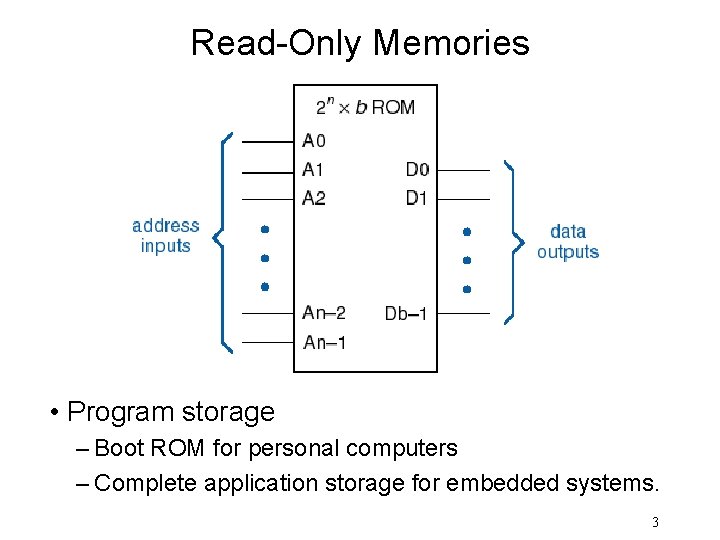
Read-Only Memories • Program storage – Boot ROM for personal computers – Complete application storage for embedded systems. 3

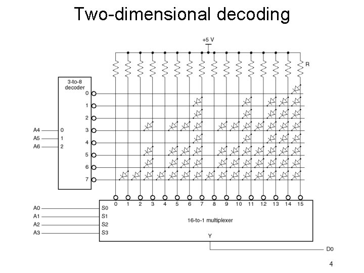
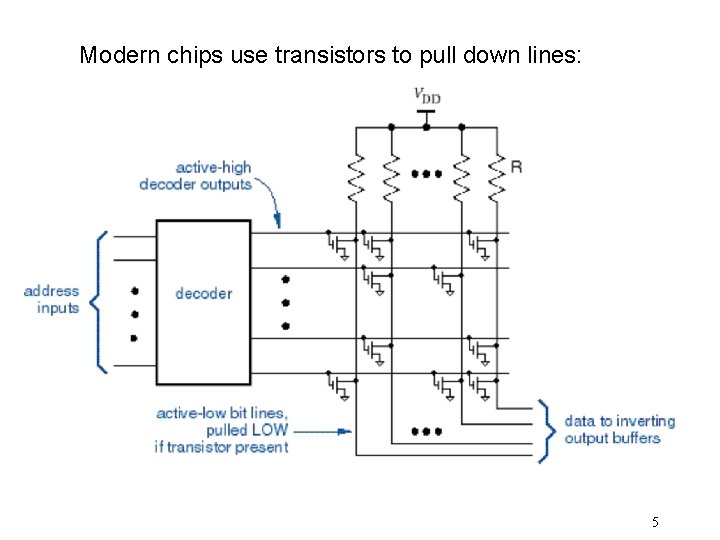
Two-dimensional decoding 4

Modern chips use transistors to pull down lines: 5

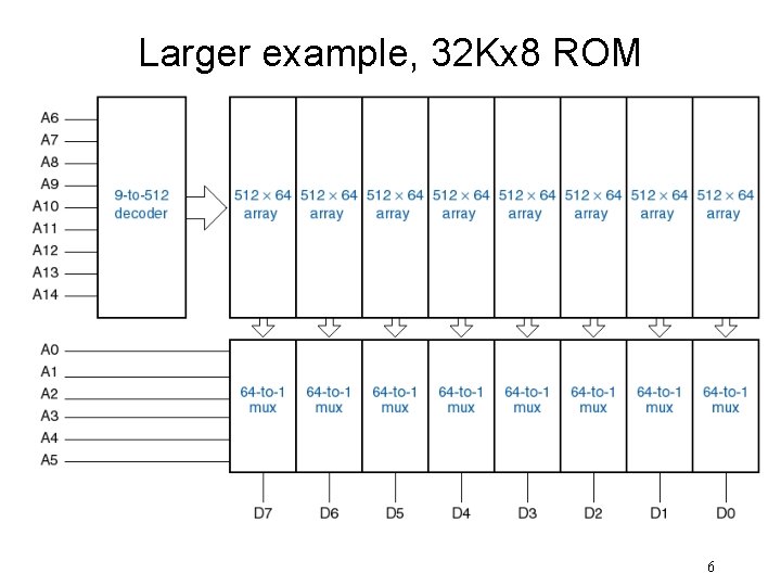
Larger example, 32 Kx 8 ROM 6

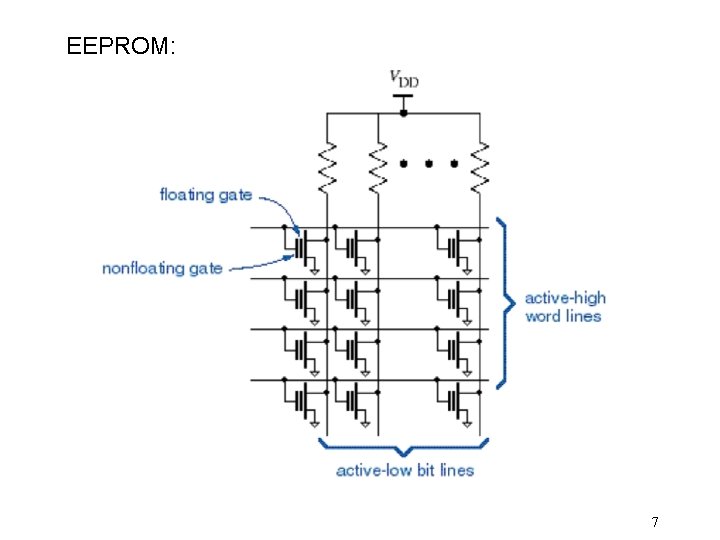
EEPROM: 7

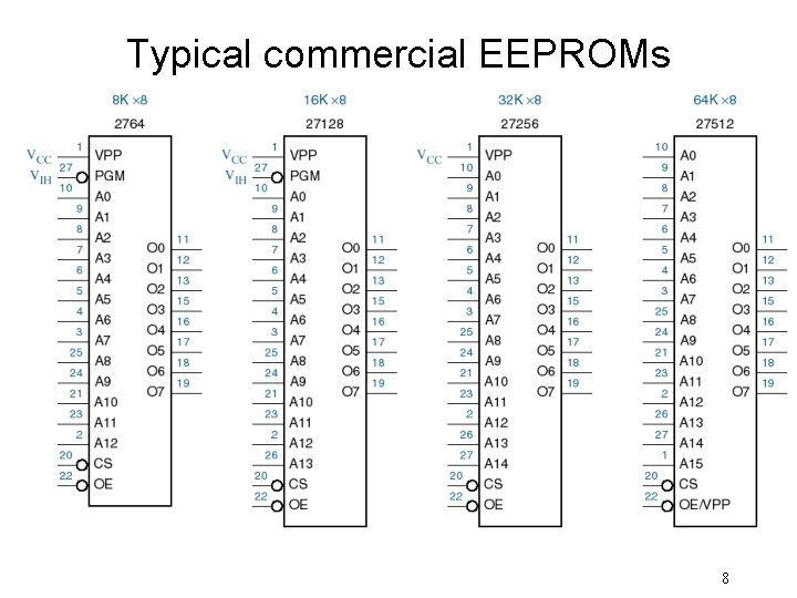
Typical commercial EEPROMs 8

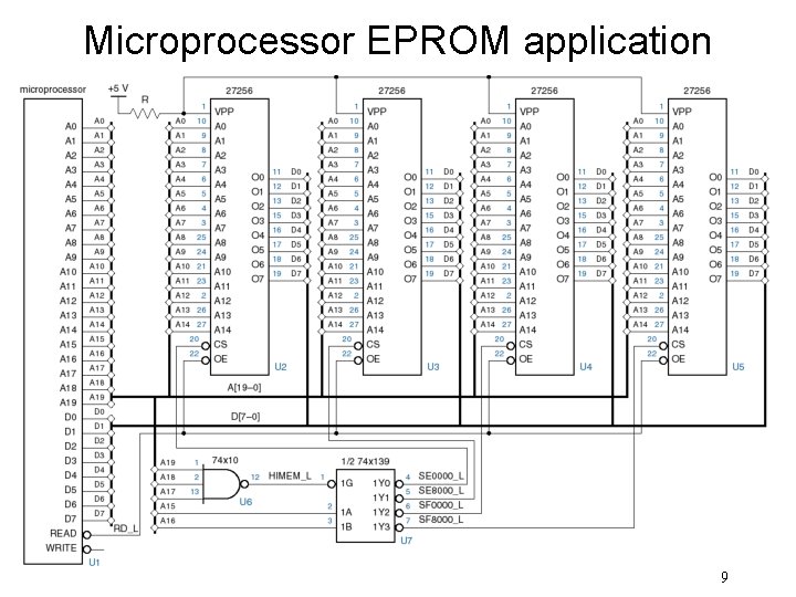
Microprocessor EPROM application 9

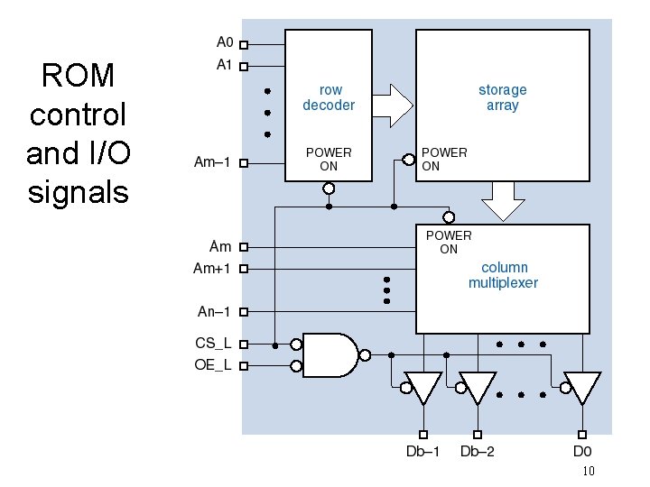
ROM control and I/O signals 10

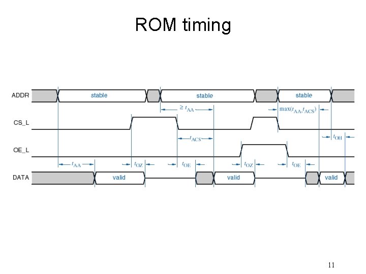
ROM timing 11

Read/Write Memories • a. k. a. “RAM” (Random Access Memory) • Volatility – Most RAMs lose their memory when power is removed – NVRAM = RAM + battery – Or use EEPROM • SRAM (Static RAM) – Memory behaves like latches or flip-flops • DRAM (Dynamic Memory) – Memory lasts only for a few milliseconds – Must “refresh” locations by reading or writing 12

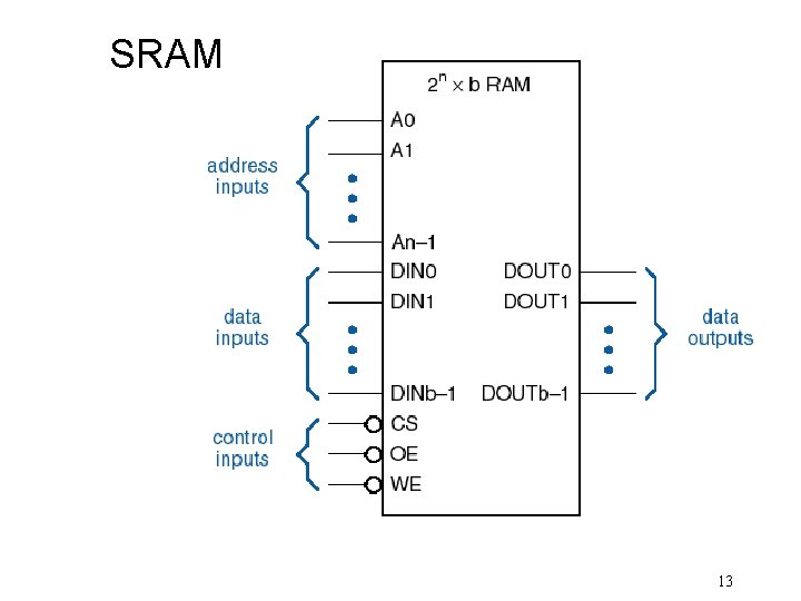
SRAM 13

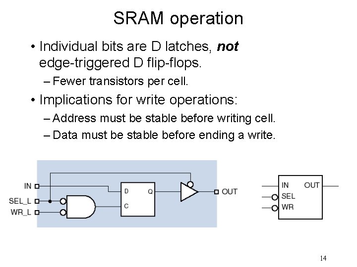
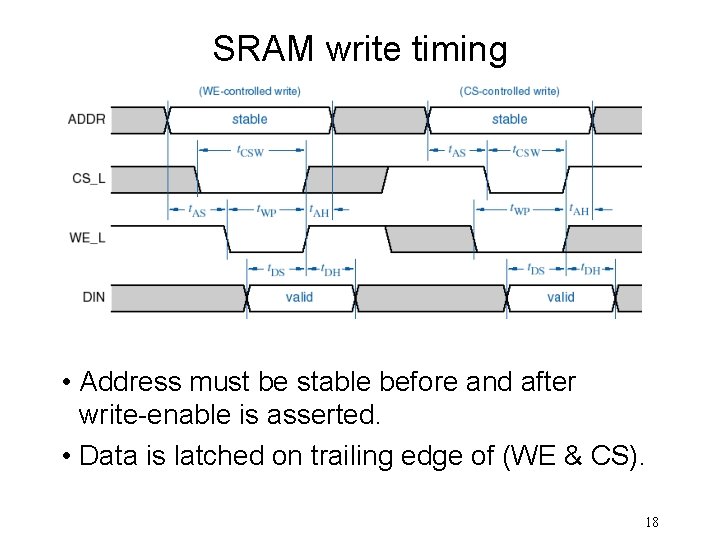
SRAM operation • Individual bits are D latches, not edge-triggered D flip-flops. – Fewer transistors per cell. • Implications for write operations: – Address must be stable before writing cell. – Data must be stable before ending a write. 14

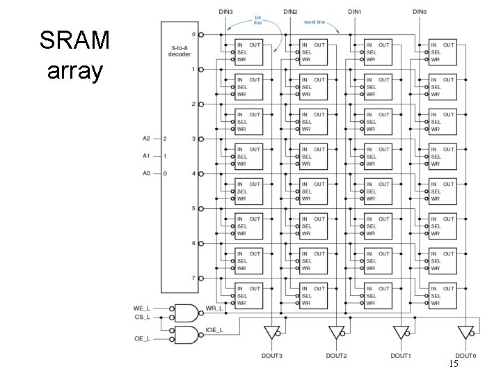
SRAM array 15

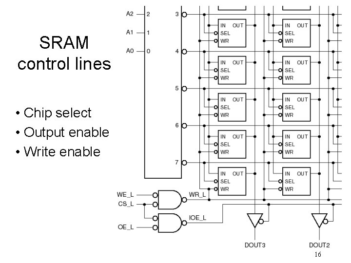
SRAM control lines • Chip select • Output enable • Write enable 16

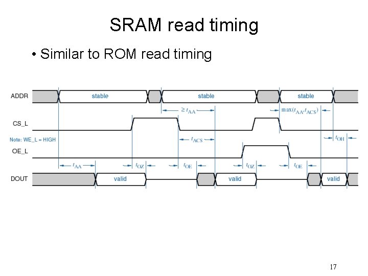
SRAM read timing • Similar to ROM read timing 17

SRAM write timing • Address must be stable before and after write-enable is asserted. • Data is latched on trailing edge of (WE & CS). 18

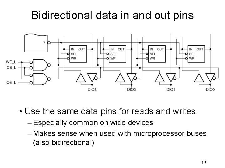
Bidirectional data in and out pins • Use the same data pins for reads and writes – Especially common on wide devices – Makes sense when used with microprocessor buses (also bidirectional) 19

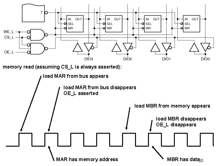
memory read (assuming CS_L is always asserted): load MAR from bus appears load MAR from bus disappears OE_L asserted load MBR from memory appears load MBR disappears OE_L disappears MAR has memory address MBR has data 20

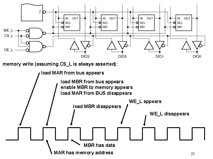
memory write (assuming CS_L is always asserted): load MAR from bus appears load MBR from bus appears enable MBR to memory appears load MAR from BUS disappears load MBR disappears WE_L disappears MBR has data MAR has memory address 21

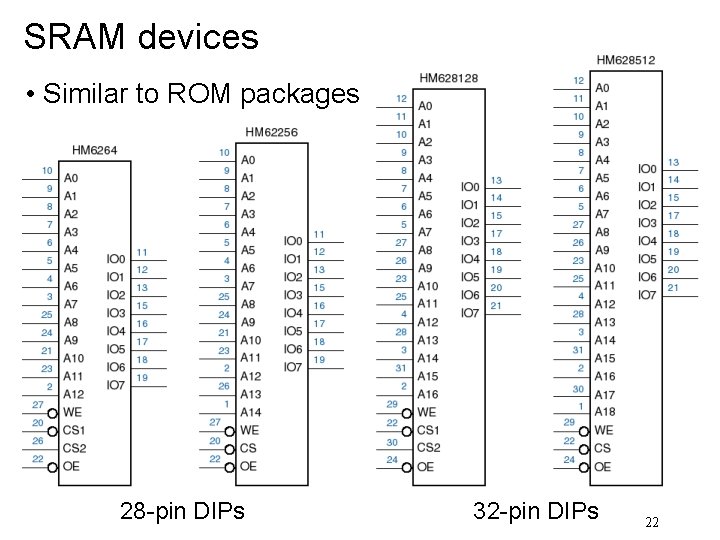
SRAM devices • Similar to ROM packages 28 -pin DIPs 32 -pin DIPs 22

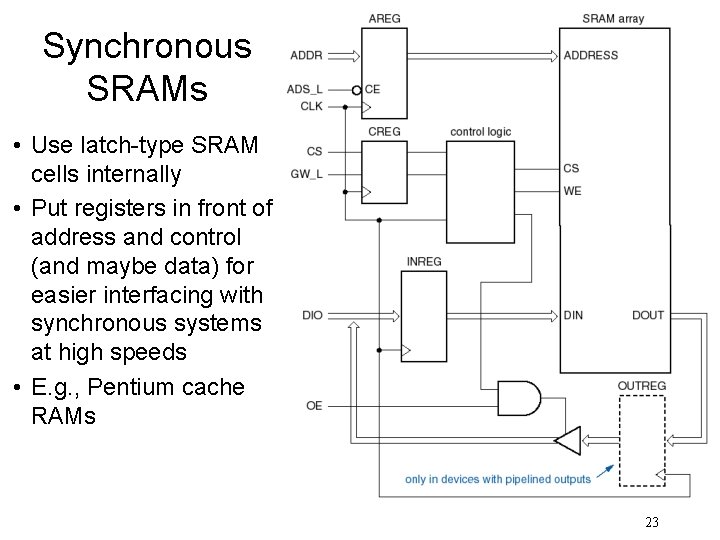
Synchronous SRAMs • Use latch-type SRAM cells internally • Put registers in front of address and control (and maybe data) for easier interfacing with synchronous systems at high speeds • E. g. , Pentium cache RAMs 23

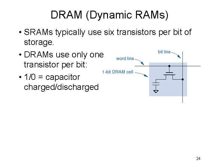
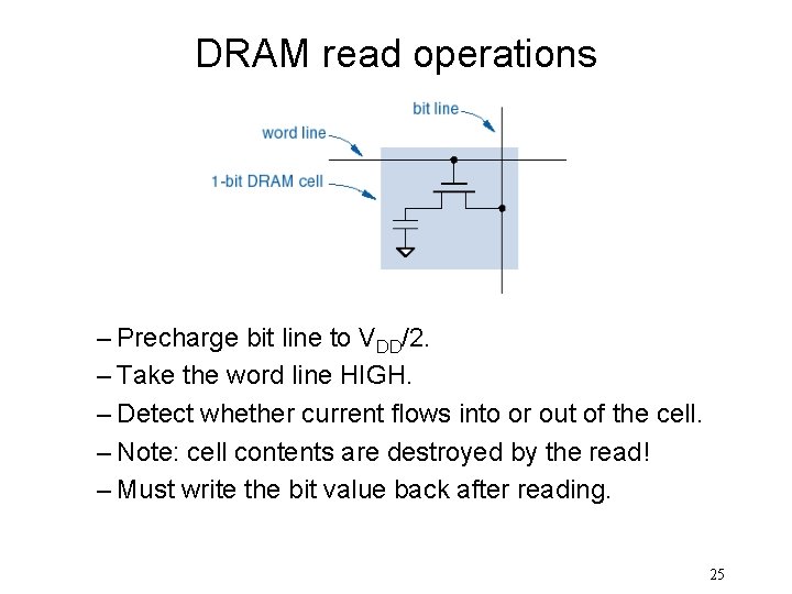
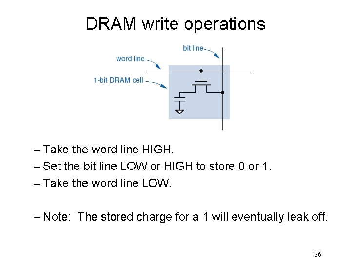
DRAM (Dynamic RAMs) • SRAMs typically use six transistors per bit of storage. • DRAMs use only one transistor per bit: • 1/0 = capacitor charged/discharged 24

DRAM read operations – Precharge bit line to VDD/2. – Take the word line HIGH. – Detect whether current flows into or out of the cell. – Note: cell contents are destroyed by the read! – Must write the bit value back after reading. 25

DRAM write operations – Take the word line HIGH. – Set the bit line LOW or HIGH to store 0 or 1. – Take the word line LOW. – Note: The stored charge for a 1 will eventually leak off. 26

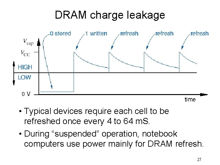
DRAM charge leakage • Typical devices require each cell to be refreshed once every 4 to 64 m. S. • During “suspended” operation, notebook computers use power mainly for DRAM refresh. 27

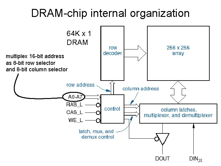
DRAM-chip internal organization 64 K x 1 DRAM multiplex 16 -bit address as 8 -bit row selector and 8 -bit column selector 28

RAS/CAS operation • Row Address Strobe, Column Address Strobe – n address bits are provided in two steps using n/2 pins, referenced to the falling edges of RAS_L and CAS_L – Traditional method of DRAM operation for 20 years. – Now being supplanted by synchronous, clocked interfaces in SDRAM (synchronous DRAM). 29

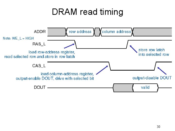
DRAM read timing 30

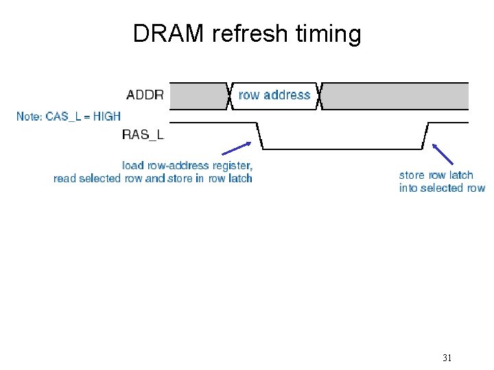
DRAM refresh timing 31

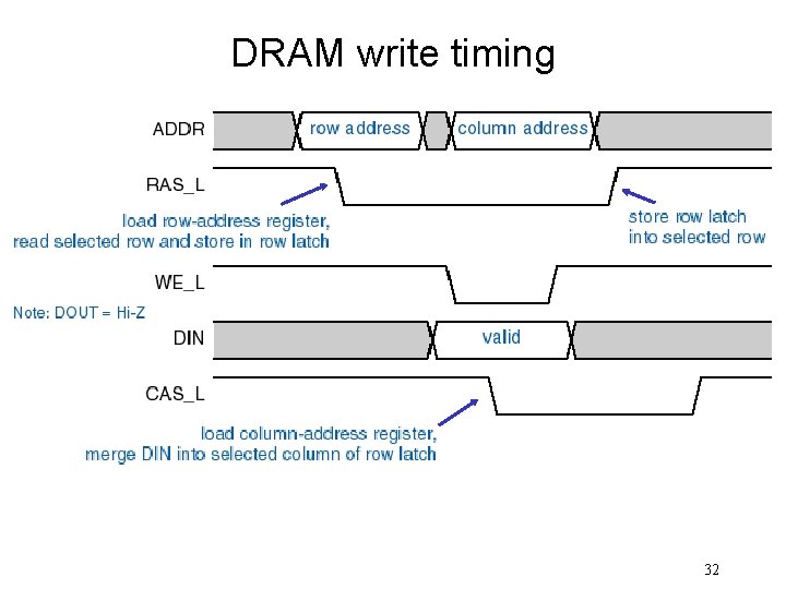
DRAM write timing 32