Thermoelectric properties of nanograting layers A Tavkhelidze Ilia



- Slides: 20

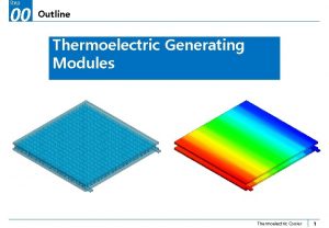
Thermoelectric properties of nanograting layers A. Tavkhelidze Ilia State University, Cholokashvili Ave. 3 -5, Tbilisi 0162, Georgia A. Tavkhelidze, Large enhancement of thermoelectric figure of merit in a ridged quantum well, Nanotechnology 20 (2009) 405401.

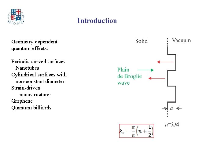
Introduction Geometry dependent quantum effects: Periodic curved surfaces Nanotubes Cylindrical surfaces with non-constant diameter Strain-driven nanostructures Graphene Quantum billiards

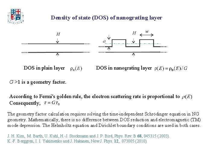
Density of state (DOS) of nanograting layer DOS in plain layer DOS in nanograting layer G >1 is a geometry factor. According to Fermi's golden rule, the electron scattering rate is proportional to Consequently, The geometry factor calculation requires solving the time-independent Schrödinger equation in NG geometry. Mathematically, there is no difference between DOS reduction and electromagnetic (TM) mode depression. The Helmholtz equation and Dirichlet boundary conditions are used in both cases. J. H. Kim, M. Barth, U. Kuhl, H. -J. Stockmann and J. P. Bird, Phys. Rev. B 68, 045315 (2003). K. -F. Berggren, I. I. Yakimenko and J. Hakanen, New J. Phys. 12, 073005 (2010).

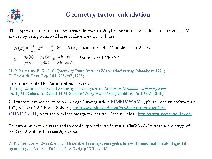
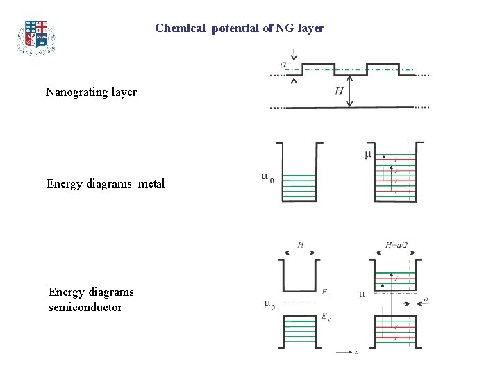
Geometry factor calculation The approximate analytical expression known as Weyl’s formula allows the calculation of TM modes by using a ratio of layer surface area and volume. is number of TM modes from 0 to k. for w=a and Hk >2. 5. H. P. Baltes and E. R. Hilf, Spectra of Finite Systems (Wissenschaftsverlag, Mannheim 1976). B. Eckhardt, Phys. Rep. 163, 205 -297 (1988). Literature related to Casimir effect, review: T. Emig, Casimir Forces and Geometry in Nanosystems, Nonlinear Dynamics of Nanosystems, ed. by G. Radons, B. Rumpf, H. G. Schuste (Wiley-VCH Verlag Gmb. H & Co. KGa. A, 2010) Software for mode calculation in ridged waveguides: FIMMMWAVE, photon design software (A fully vectorial 2 D Mode Solver), ttp: //www. photond. com/products/fimmwave. htm. CONCERTO, software for electromagnetic design, Vector Fields, http: //www. vectorfields. com. Perturbation method was used to obtain approximate formula G=(2 H-a)/2 a within the range of 3<. G<10 and for the case H, w>>a. A. Tavkhelidze, V. Svanidze and I. Noselidze, Fermi gas energetics in low-dimensional metals of special geometry, J. Vac. Sci. Technol. B, v. 25(4), p. 1270, (2007).

Chemical potential of NG layer Nanograting layer Energy diagrams metal Energy diagrams semiconductor

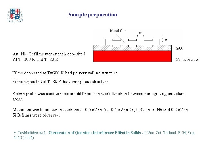
Sample preparation Au, Nb, Cr films wer quench deposited At T=300 K and T=80 K. Si substrate Films deposited at T=300 K had polycrystalline structure. Films deposited at T=80 K had amorphous structure. Kelvin probe was used to measure difference in work function between nanograting and plain areas. Maximum work function reductions of 0. 5 e. V in Au, 0. 4 e. V in Cr, 0. 35 e. V in Nb and 0. 2 e. V in Si. O 2 films were observed. A. Tavkhelidze et al. , Observation of Quantum Interference Effect in Solids , J. Vac. Sci. Technol. B 24(3), p. 1413 (2006).

AFM image of Au Nanogratilg layer

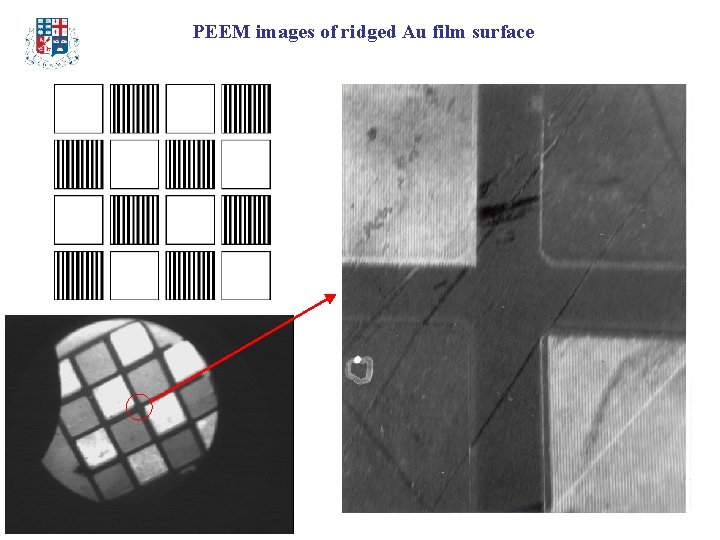
PEEM images of ridged Au film surface

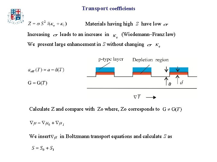
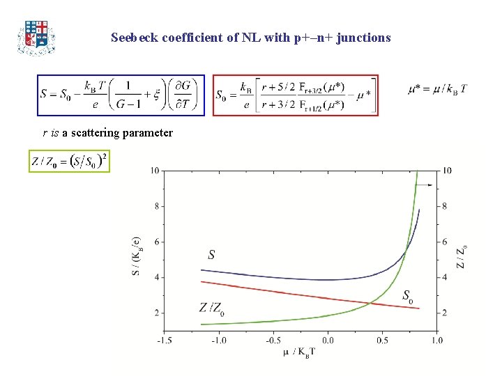
Transport coefficients Materials having high S have low Increasing leads to an increase in (Wiedemann–Franz law) We present large enhancement in S without changing Calculate Z and compare with Zo where, Zo corresponds to We insert in Boltzmann transport equations and calculate S as

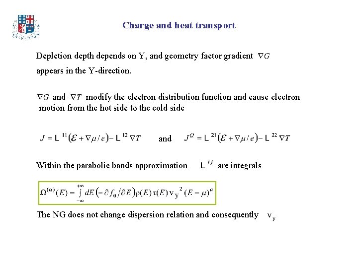
Charge and heat transport Depletion depth depends on Y, and geometry factor gradient appears in the Y-direction. and modify the electron distribution function and cause electron motion from the hot side to the cold side and Within the parabolic bands approximation are integrals The NG does not change dispersion relation and consequently

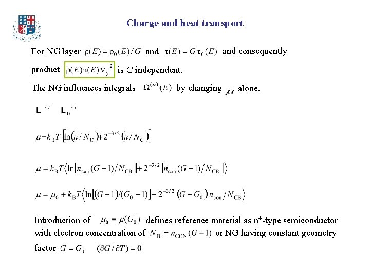
Charge and heat transport For NG layer product and consequently and is G independent. The NG influences integrals by changing alone. Introduction of defines reference material as n+-type semiconductor with electron concentration of or NG having constant geometry factor

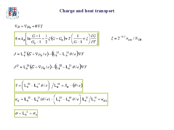
Charge and heat transport

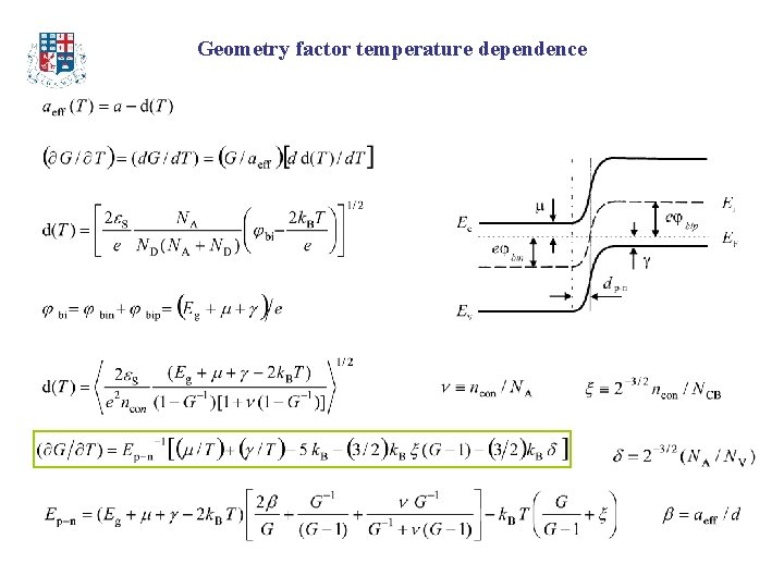
Geometry factor temperature dependence

Seebeck coefficient of NL with p+–n+ junctions r is a scattering parameter

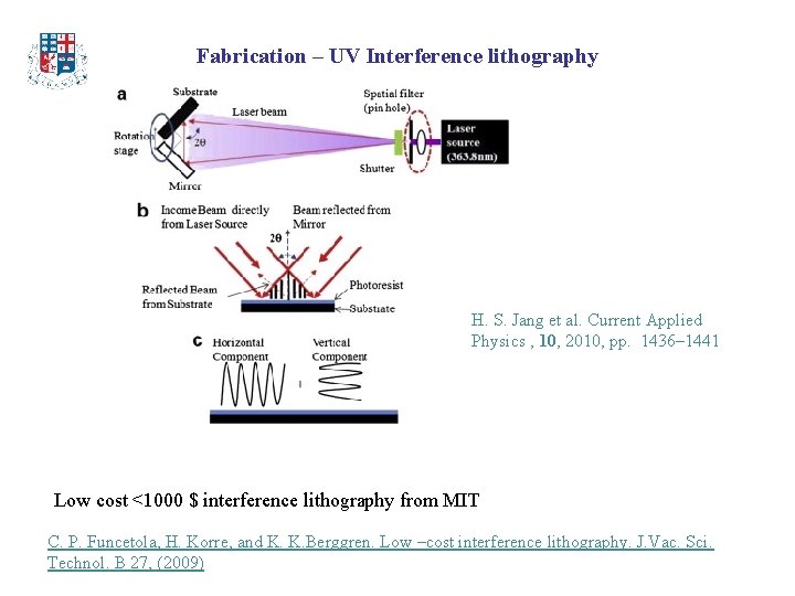
Fabrication – UV Interference lithography H. S. Jang et al. Current Applied Physics , 10, 2010, pp. 1436– 1441 Low cost <1000 $ interference lithography from MIT C. P. Funcetola, H. Korre, and K. K. Berggren. Low –cost interference lithography. J. Vac. Sci. Technol. B 27, (2009)

Preliminary experiments and results Simple Lloyd interferometer based on 405 nm laser diode. Optical microscope images of nanogratings formed in photo resist

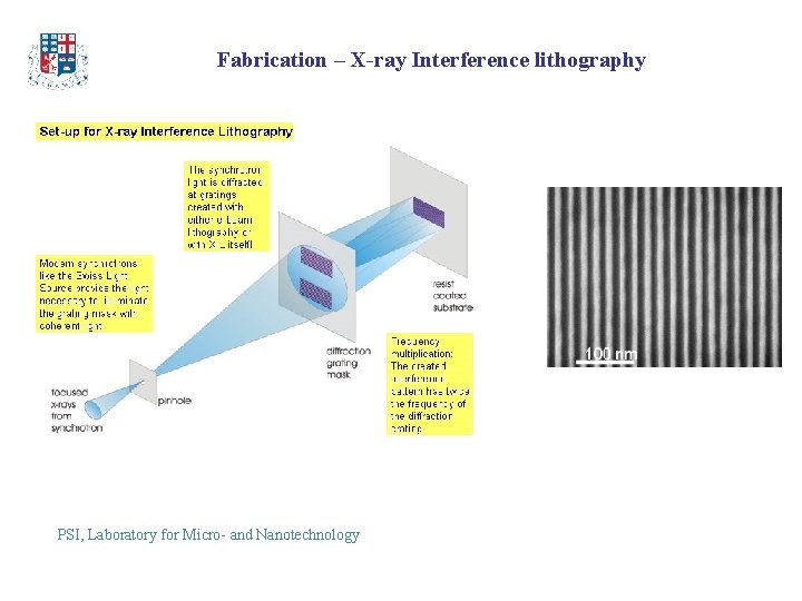
Fabrication – X-ray Interference lithography PSI, Laboratory for Micro- and Nanotechnology

Fabrication – multilayer epitaxy Cross-sectional, transmission electron microscopy micrograph of the sample grown using an interfacial superlattice with a growth rate of 1. 0 ML/ sec. The diffraction grating can be seen at the bottom of the figure and the planarized DBR layers can be seen near the top of the micrograph. G. W. Pickrell et al. , JOURNAL OF APPLIED PHYSICS V 96, 4050, 2004

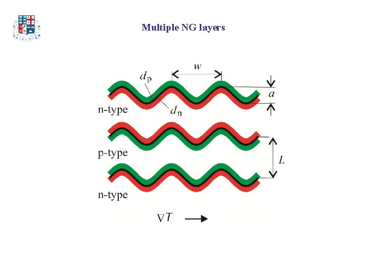
Multiple NG layers

Conclusions 1. Nanograting on the surface of thin quantum well layer reduces density of quantum states and increase chemical potential (Fermi level). 2. Work function reduction has been observed in NG films made from Au, Cr, Nb. 3. NG reduces electron scattering rates and increases electron mobility. 4. When p-n junctions are grown on the top of NG additional builds up under influence of . This leads to dramatic increase in ZT. 1. Large areas of NG having pitch of 20 nm can be fabricated using interference lithography without masks. 2. Multiple NG layers can be fabricated by epitaxial grown on NG base substrate.
 Ilia ditiatev
 Ilia sex
 Ilia musco
 Dangling bond
 Heattronics
 Incopetency
 Guided by and submitted by
 Sinda fluint
 Intensive vs extensive
 Physical property and chemical property
 Germ layers
 Fascia transversalis
 Types of crust
 Giant guinea pig
 C section layers
 Which letter indicates when dinosaurs became extinct?
 Tympanic sulcus
 The access method in bluetooth is
 #1
#1 Magnocellular layers
 Tunica albuginea

